MAX4511CSE-T中文资料
- 格式:pdf
- 大小:541.99 KB
- 文档页数:17
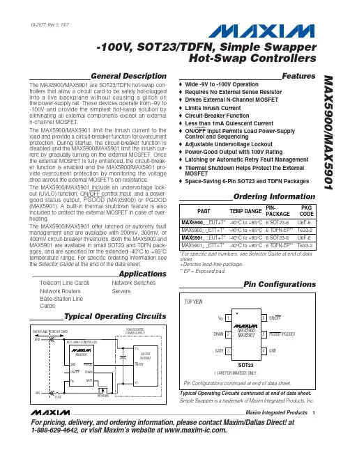
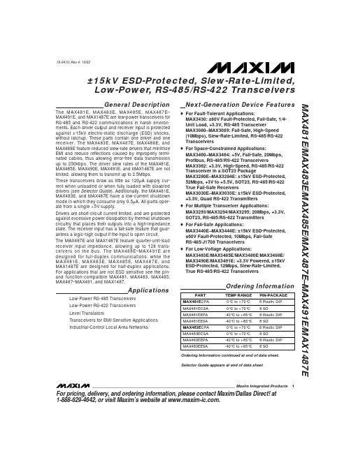
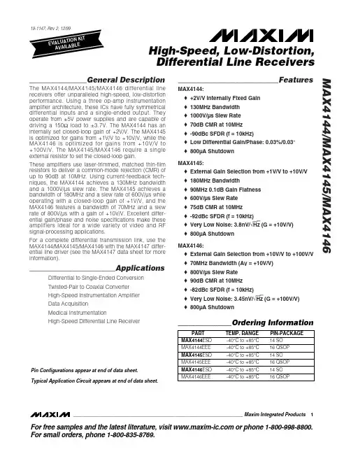
General DescriptionThe MAX4511/MAX4512/MAX4513 are quad, single-pole/single-throw (SPST), fault-protected analog switch-es. They are pin-compatible with the industry-standard nonprotected DG201/DG202/DG213. These new switch-es feature fault-protected inputs and Rail-to-Rail ®signal handling capability. The normally open (NO_) and normally closed (NC_) terminals are protected from overvoltage faults up to 36V during power-up or power-down. During a fault condition, the NO_ or NC_terminal becomes an open circuit and only nanoamperes of leakage current flow from the source, but the switch output (COM_) furnishes up to 10mA of the appropriate polarity supply voltage to the load. This ensures unam-biguous rail-to-rail outputs when a fault begins and ends.On-resistance is 175Ωmax and is matched between switches to 10Ωmax. The off-leakage current is only 0.5nA at +25°C and 10nA at +85°C.The MAX4511 has four normally closed switches. The MAX4512 has four normally open switches. The MAX4513 has two normally closed and two normally open switches.These CMOS switches can operate with dual power supplies ranging from ±4.5V to ±18V or a single supply between +9V and +36V.All digital inputs have +0.8V and +2.4V logic thresh-olds, ensuring both TTL- and CMOS-logic compatibility when using ±15V or a single +12V supply.ApplicationsFeatureso ±40V Fault Protection with Power Off±36V Fault Protection with ±15V Supplies o All Switches Off with Power Off o Rail-to-Rail Signal Handlingo Output Clamped to Appropriate Supply Voltage During Fault Condition; No Transition Glitch o 175Ωmax Signal Paths with ±15V Supplies o No Power-Supply Sequencing Required o ±4.5V to ±18V Dual Supplies +9V to +36V Single Supply o Low Power Consumption, <2mWo Four Separately Controlled SPST Switches o Pin-Compatible with Industry-StandardDG411/DG412/DG413, DG201/DG202/DG213o TTL- and CMOS-Compatible Logic Inputs with Single +9V to +15V or ±15V SuppliesFor free samples & the latest literature: , or phone 1-800-998-8800.For small orders, phone 408-737-7600 ext. 3468.MAX4511/MAX4512/MAX4513Quad, Rail-to-Rail, Fault-Protected,SPST Analog Switches________________________________________________________________Maxim Integrated Products119-4760; Rev 1; 8/02Ordering Information continued at end of data sheet.*Contact factory for dice specifications.Rail-to-Rail is a registered trademark of Nippon Motorola, Ltd.Ordering InformationPin Configurations/Functional Diagrams/Truth TablesATE Equipment Data Acquisition Industrial and Process-Control SystemsAvionicsRedundant/Backup SystemsM A X 4511/M A X 4512/M A X 4513Quad, Rail-to-Rail, Fault-Protected,SPST Analog Switches 2_______________________________________________________________________________________ABSOLUTE MAXIMUM RATINGSELECTRICAL CHARACTERISTICS—Dual Supplies(V+ = +15V, V- = -15V, GND = 0V, T A =T MIN to T MAX , unless otherwise noted. Typical values are at T A = +25°C.)Stresses beyond those listed under “Absolute Maximum Ratings” may cause permanent damage to the device. These are stress ratings only, and functional operation of the device at these or any other conditions beyond those indicated in the operational sections of the specifications is not implied. Exposure to absolute maximum rating conditions for extended periods may affect device reliability.Note 1:COM_ and IN_ pins are not fault protected. Signals on COM_ or IN_ exceeding V+ or V- are clamped by internal diodes.Limit forward diode current to maximum current rating.Note 2:NC_ and NO_ pins are fault protected. Signals on NC_ or NO_ exceeding -36V to +36V may damage the device. Theselimits apply with power applied to V+ or V-, or ±40V with V+ = V- = 0.(Voltages Referenced to GND)V+........................................................................-0.3V to +44.0V V-.........................................................................-44.0V to +0.3V V+ to V-................................................................-0.3V to +44.0V COM_, IN_ (Note 1)..............................(V- - 0.3V) to (V+ + 0.3V)NC_, NO_ (Note 2)..................................(V+ - 36V) to (V- + 36V)NC_, NO_ to COM_.................................................-36V to +36V Continuous Current into Any Terminal..............................±30mA Peak Current into Any Terminal(pulsed at 1ms, 10% duty cycle)...................................±50mAContinuous Power Dissipation (T A = +70°C) (Note 2)Plastic DIP (derate 10.53mW/°C above +70°C)...........842mW Narrow SO (derate 8.70mW/°C above +70°C).............696mW TSSOP (derate 9.4mW/°C above +70°C)..................754.7mW CERDIP (derate 10.00mW/°C above +70°C)................800mW Operating Temperature RangesMAX451_C_ E......................................................0°C to +70°C MAX451_E_ E...................................................-40°C to +85°C MAX451_MJE .................................................-55°C to +125°C Storage Temperature Range.............................-65°C to +150°C Lead Temperature (soldering, 10s).................................+300°CMAX4511/MAX4512/MAX4513Quad, Rail-to-Rail, Fault-Protected,SPST Analog Switches_______________________________________________________________________________________3ELECTRICAL CHARACTERISTICS—Dual Supplies (continued)(V+ = +15V, V- = -15V, GND = 0V, T A =T MIN to T MAX , unless otherwise noted. Typical values are at T A = +25°C.)M A X 4511/M A X 4512/M A X 4513Quad, Rail-to-Rail, Fault-Protected,SPST Analog Switches 4_______________________________________________________________________________________ELECTRICAL CHARACTERISTICS—Dual Supplies (continued)(V+ = +15V, V- = -15V, GND = 0V, T A = T MIN to T MAX , unless otherwise noted. Typical values are at T A = +25°C.)MAX4511/MAX4512/MAX4513Quad, Rail-to-Rail, Fault-Protected,SPST Analog Switches_______________________________________________________________________________________5ELECTRICAL CHARACTERISTICS—Single +12V Supply(V+ = +10.8V to +13.2V, V- = 0, T A = T MIN to T MAX , unless otherwise noted. Typical values are at T A = +25°C.)M A X 4511/M A X 4512/M A X 4513Quad, Rail-to-Rail, Fault-Protected,SPST Analog Switches 6_______________________________________________________________________________________Note 1:COM_ and IN_ pins are not fault protected. Signals on COM_ or IN_ exceeding V+ or V- are clamped by internal diodes.Limit forward diode current to maximum current rating.Note 2:NC_ and NO_ pins are fault protected. Signals on NC_ or NO_ exceeding -36V to +36V may damage the device. These limits apply with power applied to V+ or V-, or ±40V with V+ = V- = 0.Note 3:The algebraic convention is used in this data sheet; the most negative value is shown in the minimum column.Note 4:∆R ON = ∆R ON(MAX)- ∆R ON(MIN).Note 5:Leakage parameters are 100% tested at maximum rated hot temperature and guaranteed by correlation at T A = +25°C.Note 6:Guaranteed by design.Note 7:Off isolation = 20 log10 [ V COM_/ (V NC_or V NO_) ], V COM_= output, V NC_or V NO_= input to off switch.Note 8:Between any two switches.Note 9:Leakage testing for single-supply operation is guaranteed by testing with dual supplies.ELECTRICAL CHARACTERISTICS—Single +12V Supply (continued)(V+ = +10.8V to +13.2V, V- = 0, T A = T MIN to T MAX , unless otherwise noted. Typical values are at T A = +25°C.)MAX4511/MAX4512/MAX4513Quad, Rail-to-Rail, Fault-Protected,SPST Analog Switches_______________________________________________________________________________________7__________________________________________Typical Operating Characteristics(T A = +25°C, unless otherwise noted.)010050250200150300350-20-50-15-105101520SWITCH ON-RESISTANCE vs. V COM (DUAL SUPPLIES)V COM (V)S W I T C H O N -R E S I S T A N C E (Ω)80602040160140100120180200-15-50-1051015SWITCH ON-RESISTANCE vs. V COM AND TEMPERATURE (DUAL SUPPLIES)V COM (V)S W I T C H O N -R E S I S T A N C E (Ω)100010051015202530SWITCH ON-RESISTANCE vs. V COM (SINGLE SUPPLY)V COM (V)S W I T C H O N -R E S I S I T A N C E (Ω)050200150100300350250400046281012SWITCH ON-RESISTANCE vs. V COM AND TEMPERATURE (SINGLE SUPPLY)V COM (V)S W I T C H O N -R E S I S T A N C E (Ω)0300200100700800600500400900100005101520ON AND OFF TIMES vs. SUPPLY VOLTAGESUPPLY VOLTAGE (±V)t O N , t O F F (n s )1p10p100p1n10n 100n-50-25255075100125150I D(ON), I S(OFF), AND I D(OFF) LEAKAGES vs. TEMPERATURETEMPERATURE (°C)L E A K A G E (A )02810641214-15-10-5051015CHARGE INJECTION vs. V COM (DUAL SUPPLIES)V COM (V)Q (p C )010*******500400600-5025-255075100125ON AND OFF TIMES vs. TEMPERATURETEMPERATURE (°C)t O N , t O F F (n s )100300200500400600-50025-255075100125POWER-SUPPLY CURRENT vs. TEMPERATURETEMPERATURE (°C)S U P P L Y C U R R E N T (µA )M A X 4511/M A X 4512/M A X 4513Quad, Rail-to-Rail, Fault-Protected,SPST Analog Switches 8_______________________________________________________________________________________00.51.51.02.52.03.001015520253035LOGIC-LEVEL THRESHOLD vs. V+M A X 4511-10V+ (V)L O G I C -L E V E L T H R E S H O L D (V )Typical Operating Characteristics (continued)(T A = +25°C, unless otherwise noted.)0-10-20-1200.010.11101001000FREQUENCY RESPONSE-90-100-110FREQUENCY (MHz)L O S S (d B )P H A S E (D E G R E E S )-70-80-50-60-30-4012010080-120-60-80-100-20-402006040Pin Description*As long as the voltage on NO_ or NC_ does not exceed V+ or V-, NO_ (or NC_) and COM_ pins are identical and interchange-able. Either may be considered as an input or output; signals pass equally well in either direction.Detailed DescriptionOverview of Traditional Fault-Protected SwitchesThe MAX4511/MAX4512/MAX4513 are fault-protected CMOS analog switches with unusual operation and construction. Traditional fault-protected switches are constructed by three series FETs. This produces good off characteristics, but fairly high on-resistance when the signals are within about 3V of each supply rail. As the voltage on one side of the switch approaches with-in about 3V of either supply rail (a fault condition), the switch impedance becomes higher, limiting the output signal range (on the protected side of the switch) to approximately 3V less than the appropriate polarity supply voltage.During a fault condition, the output current that flows from the protected side of the switch into its load comes from the fault source on the other side of the switch. I f the switch is open or the load is extremely high impedance, the input current will be very low. I f the switch is on and the load is low impedance,enough current will flow from the source to maintain the load voltage at 3V less than the supply.MAX4511/MAX4512/MAX4513Quad, Rail-to-Rail, Fault-Protected,SPST Analog Switches_______________________________________________________________________________________9Overview of MAX4511/MAX4512/MAX4513The MAX4511/MAX4512/MAX4513 differ considerably from traditional fault-protection switches, with several advantages. First, they are constructed with two paral-lel FETs, allowing very low on-resistance when the switch is on. Second, they allow signals on the NC_ or NO_ pins that are within or slightly beyond the supply rails to be passed through the switch to the COM termi-nal, allowing rail-to-rail signal operation. Third, when a signal on NC_ or NO_ exceeds the supply rails by about 50mV (a fault condition), the voltage on COM_ is limited to the appropriate polarity supply voltage.Operation is identical for both fault polarities. The fault-protection extends to ±36V from GND.During a fault condition, the NO_ or NC_ input pin becomes high impedance regardless of the switch state or load resistance. If the switch is on, the COM_output current is furnished from the V+ or V- pin by “booster” FETs connected to each supply pin. These FETs can typically source or sink up to 10mA.When power is removed, the fault protection is still in effect. In this case, the NO_ or NC_ terminals are a vir-tual open circuit. The fault can be up to ±40V.The COM_ pins are not fault protected; they act as nor-mal CMOS switch pins. If a voltage source is connect-ed to any COM_ pin, it should be limited to the supply voltages. Exceeding the supply voltage will cause high currents to flow through the ESD protection diodes,possibly damaging the device (see Absolute Maximum Ratings ).Pin CompatibilityThese switches have identical pinouts to common non-fault-protected CMOS switches. Care should be exer-cised in considering them for direct replacements in existing printed circuit boards, however, since only the NO_ and NC_ pins of each switch are fault protected.Internal ConstructionInternal construction is shown in Figure 1, with the ana-log signal paths shown in bold. A single normally openFigure 1. Block DiagramM A X 4511/M A X 4512/M A X 4513Quad, Rail-to-Rail, Fault-Protected,SPST Analog Switches 10______________________________________________________________________________________(NO) switch is shown; the normally closed (NC) config-uration is identical except the logic-level translator becomes an inverter. The analog switch is formed by the parallel combination of N-channel FET N1 and P-channel FET P1, which are driven on and off simultane-ously according to the input fault condition and the logic-level state.Normal OperationTwo comparators continuously compare the voltage on the NO_ (or NC_) pin with V+ and V-. When the signal on NO_ or NC_ is between V+ and V- the switch acts normally, with FETs N1 and P1 turning on and off in response to I N_ signals. The parallel combination of N1 and P1 forms a low-value resistor between NO_ (or NC_) and COM_ so that signals pass equally well in either direction.Positive Fault ConditionWhen the signal on NO_ (or NC_) exceeds V+ by about 50mV, the high-fault comparator output is high, turning off FETs N1 and P1. This makes the NO_ (or NC_) pin high impedance regardless of the switch state. I f the switch state is “off”, all FETs are turned off and both NO_ (or NC_) and COM_ are high impedance. I f the switch state is “on”, FET P2 is turned on, sourcing cur-rent from V+ to COM_.Negative Fault ConditionWhen the signal on NO_ (or NC_) exceeds V- by about 50mV, the low-fault comparator output is high, turning off FETs N1 and P1. This makes the NO_ (or NC_) pin high impedance regardless of the switch state. I f the switch state is “off,” all FETs are turned off and both NO_ (or NC_) and COM_ are high impedance. I f the switch state is “on,” FET N2 is turned on, sinking cur-rent from COM_ to V-.Transient Fault Response and RecoveryWhen a fast rise-time and fall-time transient on I N_exceeds V+ or V-, the output (COM_) follows the input (I N_) to the supply rail with only a few nanoseconds delay. This delay is due to the switch on-resistance and circuit capacitance to ground. When the input transient returns to within the supply rails, however, there is a longer output recovery time delay. For positive faults, the recovery time is typically 3.5µs. For negative faults, the recovery time is typically 1.3µs. These values depend on the COM_ output resistance and capacitance, and are not production tested or guaranteed. The delays are not dependent on the fault amplitude. Higher COM_ output resistance and capacitance increase recovery times.COM_ and IN_ PinsFETs N2 and P2 can source about ±10mA from V+ or V-to the COM_ pin in the fault condition. Ensure that if the COM_ pin is connected to a low-resistance load, the absolute maximum current rating of 30mA is never exceeded, both in normal and fault conditions.The GND, COM_, and IN_ pins do not have fault protec-tion. Reverse ESD-protection diodes are internally con-nected between GND, COM_, IN_ and both V+ and V-. If a signal on GND, COM_, or I N_ exceeds V+ or V- by more than 300mV, one of these diodes will conduct heavily. During normal operation these reverse-biased ESD diodes leak a few nanoamps of current to V+ and V-.Fault-Protection Voltage and Power OffThe maximum fault voltage on the NC_ or NO_ pins is ±36V with power applied and ±40V with power off.Failure ModesThe MAX4511/MAX4512/MAX4513 are not lightning arrestors or surge protectors.Exceeding the fault-protection voltage limits on NO_ or NC_, even for very short periods, can cause the device to fail. The failure modes may not be obvious, and fail-ure in one switch may or may not affect other switches in the same package.GroundThere is no connection between the analog signal paths and GND. The analog signal paths consist of an N-channel and P-channel MOSFET with their sources and drains paralleled and their gates driven out of phase to V+ and V- by the logic-level translators.V+ and GND power the internal logic and logic-level translators and set the input logic thresholds. The logic-level translators convert the logic levels to switched V+and V- signals to drive the gates of the analog switch-es. This drive signal is the only connection between the power supplies and the analog signals. GND, IN_, and COM_ have ESD-protection diodes to V+ and V-.IN_ Logic-Level ThresholdsThe logic-level thresholds are CMOS and TTL compati-ble when V+ is +15V. As V+ is raised the threshold increases slightly, and when V+ reaches 25V the level threshold is about 2.8V—above the TTL output high level minimum of 2.4V, but still compatible with CMOS outputs (see Typical Operating Characteristics ).Increasing V- has no effect on the logic-level thresholds,but it does increase the gate-drive voltage to the signal FETs, reducing their on-resistance.MAX4511/MAX4512/MAX4513Quad, Rail-to-Rail, Fault-Protected,SPST Analog Switches______________________________________________________________________________________11Bipolar SuppliesThe MAX4511/MAX4512/MAX4513 operate with bipolar supplies between ±4.5V and ±18V. The V+ and V- sup-plies need not be symmetrical, but their difference can not exceed the absolute maximum rating of 44V.Single SupplyThe MAX4511/MAX4512/MAX4513 operate from a sin-gle supply between +9V and +36V when V- is connect-ed to GND.High-Frequency PerformanceIn 50Ωsystems, signal response is reasonably flat up to 50MHz (see Typical Operating Characteristics ). Above20MHz, the on-response has several minor peaks that are highly layout dependent. The problem with high-fre-quency operation is not turning the switch on, but turn-ing it off. The off-state switch acts like a capacitor and passes higher frequencies with less attenuation. At 10MHz, off isolation is about -42dB in 50Ωsystems,becoming worse (approximately 20dB per decade) as frequency increases. Higher circuit impedances also make off isolation worse. Adjacent channel attenuation is about 3dB above that of a bare IC socket and is due entirely to capacitive coupling.Figure 2. Switch Turn-On/Turn-Off TimesTest Circuits/Timing DiagramsFigure 3. MAX4513 Break-Before-Make IntervalM A X 4511/M A X 4512/M A X 4513Quad, Rail-to-Rail, Fault-Protected,SPST Analog Switches 12______________________________________________________________________________________Figure 4. Charge InjectionFigure 5. COM_, NO_, NC_ CapacitanceTest Circuits/Timing Diagrams (continued)MAX4511/MAX4512/MAX4513Quad, Rail-to-Rail, Fault-Protected,SPST Analog Switches______________________________________________________________________________________13Figure 6. Frequency Response, Off Isolation, and CrosstalkTest Circuits/Timing Diagrams (continued)Pin Configurations/Functional Diagrams/Truth Tables (continued)M A X 4511/M A X 4512/M A X 4513Quad, Rail-to-Rail, Fault-Protected,SPST Analog Switches 14______________________________________________________________________________________V-GNDNC4COM4IN4IN3COM30.086"(2.261mm)MAX4511NO1NO2COM1IN1IN2COM2COM4NO4IN4IN3NO3COM30.086"(2.261mm)MAX4512Ordering Information (continued)Chip TopographiesV-GNDCOM4NO4IN4IN3NC3COM3MAX45130.086"(2.261mm)TRANSISTOR COUNT: 139SUBSTRATE CONNECTED TO:V+*Contact factory for dice specifications.MAX4511/MAX4512/MAX4513Quad, Rail-to-Rail, Fault-Protected,SPST Analog Switches______________________________________________________________________________________15Package Information(The package drawing(s) in this data sheet may not reflect the most current specifications. For the latest package outline information,go to /packages .)M A X 4511/M A X 4512/M A X 4513Quad, Rail-to-Rail, Fault-Protected,SPST Analog Switches 16______________________________________________________________________________________Package Information (continued)(The package drawing(s) in this data sheet may not reflect the most current specifications. For the latest package outline information,go to /packages.)MAX4511/MAX4512/MAX4513Quad, Rail-to-Rail, Fault-Protected,SPST Analog SwitchesMaxim cannot assume responsibility for use of any circuitry other than circuitry entirely embodied in a Maxim product. No circuit patent licenses are implied. Maxim reserves the right to change the circuitry and specifications without notice at any time.Maxim Integrated Products, 120 San Gabriel Drive, Sunnyvale, CA 94086 408-737-7600______________________17©2002 Maxim Integrated ProductsPrinted USAis a registered trademark of Maxim Integrated Products.Package Information (continued)(The package drawing(s) in this data sheet may not reflect the most current specifications. For the latest package outline information,go to /packages .)。