
35363-0460;中文规格书,Datasheet资料
- 格式:pdf
- 大小:294.16 KB
- 文档页数:4

NCV8450, NCV8450ASelf-Protected High Side Driver with Temperatureand Current LimitThe NCV8450/A is a fully protected High−Side Smart Discrete device with a typical R DS(on) of 1.0 W and an internal current limit of 0.8 A typical. The device can switch a wide variety of resistive, inductive, and capacitive loads.Features•Short Circuit Protection•Thermal Shutdown with Automatic Restart •Overvoltage Protection•Integrated Clamp for Inductive Switching•Loss of Ground Protection•ESD Protection•Slew Rate Control for Low EMI•Very Low Standby Current•NCV Prefix for Automotive and Other Applications Requiring Unique Site and Control Change Requirements; AEC−Q100 Qualified and PPAP Capable•This is a Pb−Free DeviceTypical Applications•Automotive•IndustrialPRODUCT SUMMARYSymbolCharacteristics Value Unit V IN_CL Overvoltage Protection54V V D(on)Operation Voltage 4.5 − 45V R on On−State Resistance 1.0WMARKINGDIAGRAM1AYWXXXXX GGXXXXX= V8450 or 8450AA= Assembly LocationY= YearW= Work WeekG= Pb−Free Package(Note: Microdot may be in either location)SOT−223(TO−261)CASE 318ESee detailed ordering and shipping information in the package dimensions section on page 8 of this data sheet.ORDERING INFORMATIONFigure 1. Block Diagram V (Pins 2, 4)OUT(Pin 3)IN(Pin 1)PACKAGE PIN DESCRIPTIONPin #Symbol Description1IN Control Input, Active Low2V D Supply Voltage3OUT Output4V D Supply VoltageMAXIMUM RATINGSRatingSymbol ValueUnit Min Max DC Supply Voltage (Note 1)V D −1645V Load Dump Protection(RI = 2 W , t d = 400 ms, V IN = 0, 10 V, I L = 150 mA, V bb = 13.5 V)V Loaddump100V Input CurrentIin −1515mAOutput Current (Note 1)I out Internally Limited A Total Power Dissipation@ T A = 25°C (Note 2)@ T A = 25°C (Note 3)P D1.131.60WElectrostatic Discharge (Note 4)(Human Body Model (HBM) 100 pF/1500 W )Input All other15kVSingle Pulse Inductive Load Switching Energy (Note 4)(V DD = 13.5 V, I = 465 mApk, L = 200 mH, T JStart = 150°C)E AS 29mJ Operating Junction Temperature T J −40+150°C Storage TemperatureT storage−55+150°CStresses exceeding Maximum Ratings may damage the device. Maximum Ratings are stress ratings only. Functional operation above the Recommended Operating Conditions is not implied. Extended exposure to stresses above the Recommended Operating Conditions may affect device reliability.1.Reverse Output current has to be limited by the load to stay within absolute maximum ratings and thermal performance.2.Minimum Pad.3. 1 in square pad size, FR −4, 1 oz Cu.4.Not subjected to production testing.THERMAL RESISTANCE RATINGSParameterSymbol Max Value Unit Thermal Resistance (Note 5)Junction −to −Ambient (Note 2)Junction −to −Ambient (Note 3)R q JA R q JA11078.3K/W5.Not subjected to production testing.Figure 2. Applications Test CircuitELECTRICAL CHARACTERISTICS (6 v V D v 45 V; −40°C <T J < 150°C unless otherwise specified)Rating Symbol ConditionsValueUnit Min Typ MaxOUTPUT CHARACTERISTICSOperating Supply Voltage V SUPPLY 4.5−45VOn Resistance(Pin 1 Connected to GND)R ON T J = 25°C , I OUT = 150 mA, V D = 7 V − 45 VT J = 150°C, I OUT = 150 mA, V D = 7 V − 45 V(Note 6)T J = 25°C , I OUT= 150 mA, V D = 6 V1.01.41.1232.1WStandby Current (Pin 1 Open)I D V D v 20 VV D> 20 V 0.610100m AINPUT CHARACTERISTICSInput Current – Off State I IN_OFF V OUT v 0.1 V, R L = 270 W, T J = 25°CV OUT v 0.1V, R L= 270 W, T J = 150°C (Note 6)−50−40m AInput Current – On State(Pin 1 Grounded)I IN_ON 1.53mA Input Resistance (Note 6)R IN1k W SWITCHING CHARACTERISTICSTurn−On Time (Note 7)(V IN = V D to 0 V) to 90% V OUT t ON R L = 270 W(Note 6)V D = 13.5 V, R L = 270 W, T J = 25°C30125100m sTurn−Off Time (Note 7)(V IN= 0 V to V D) to 10% V OUT t OFF R L = 270 W (Note 6)V D = 13.5 V, R L = 270 W, T J = 25°C60175150m sSlew Rate On (Note 7)(V IN = V D to 0V) 10% to 30% V OUT dV/dt ON R L = 270 W(Note 6)V D = 13.5 V, R L = 270 W, T J = 25°C0.744V/m sSlew Rate Off (Note 7)(V IN= 0 V to V D) 70% to 40% V OUT dV/dt OFF R L = 270 W (Note 6)V D = 13.5 V, R L = 270 W, T J = 25°C0.944V/m sOUTPUT DIODE CHARACTERISTICS (Note 6)Drain−Source Diode Voltage V F I OUT = −0.2 A0.6V Continuous Reverse DrainCurrentI S T J = 25°C0.2A PROTECTION FUNCTIONS (Note 8)Temperature Shutdown (Note 6)T SD150175−°C Temperature ShutdownHysteresis (Note 6)T SD_HYST5°COutput Current Limit I LIM T J = −40°C, V D = 13.5 V, t m = 100 m s (Note 6)T J = 25 °C, V D = 13.5 V, t m = 100 m sT J = 150 °C , V D = 13.5 V, t m = 100 m s (Note 6)0.50.81.5AOutput Clamp Voltage(Inductive Load Switch Off)At V OUT = V D− V CLAMPV CLAMP I OUT = 4 mA4552VOvervoltage Protection V IN_CL I CLAMP = 4 mA5054V6.Not subjected to production testing7.Only valid with high input slew rates8.Protection functions are not designed for continuous repetitive operation and are considered outside normal operating rangeR D S (o n ) (W )TEMPERATURE (°C)Figure 3. R DS(on) vs. TemperatureR D S (o n ) (W )OUTPUT LOAD (A)Figure 4. R DS(on) vs. Output LoadV D (V)Figure 5. R DS(on) vs. V DR D S (o n ) (W )1020304050607080T U R N O N T I M E (m s )TEMPERATURE (°C)Figure 6. Turn On Time vs. TemperatureTEMPERATURE (°C)Figure 7. Turn Off Time vs. TemperatureT U R N O F F T I M E (m s )S L E W R A T E (O N ) (V /m s )TEMPERATURE (°C)Figure 8. Slew Rate (ON) vs. Temperature−40−20020406080100120140−40−20020406080100120140−TEMPERATURE (°C)Figure 9. Slew Rate (OFF) vs. Temperature S L E W R A T E (O F F ) (V /m s )TEMPERATURE (°C)Figure 10. Current Limit vs. TemperatureC U R R E N T L I M I T (A )P E A K S C C U R R E N T (A )V D , VOLTAGE (V)Figure 11. Peak Short Circuit Current vs. V DVoltageTEMPERATURE (°C)Figure 12. V D Leakage Current vs.Temperature Off −StateV D , L E A K A G E C U R R E N T (m A )V D , L E A K A G E C U R R E N T (m A )V D , VOLTAGE (V)Figure 13. V D Leakage Current vs. V D VoltageOff −State TEMPERATURE (°C)Figure 14. On −State Input Current vs.TemperatureI N P U T C U R R E N T (m A )V D , VOLTAGE (V)Figure 15. Output Voltage vs. V D VoltageO U T P U T V O L T A G E (V )V D , VOLTAGE (V)Figure 16. Input Current vs. V D VoltageOn −StateI N P U T C U R R E N T (m A )LOAD INDUCTANCE (mH)Figure 17. Single Pulse Maximum Switch −offCurrent vs. Load InductanceC U R R E N T (m A )V D , VOLTAGE (V)Figure 18. Input Current vs. V D VoltageOff −StateI N P U T C U R R E N T (m A )−S H U T D O W N T I M E (m s )TEMPERATURE (°C)Figure 19. Initial Short −Circuit Shutdown Timevs. TemperaturePULSE TIME (s)R (t ), E F F E C T I V E T R A N S I E N T T H E R M AL R E S P O N S ECOPPER HEAT SPREADER AREA (mm 2)R q J A (°C /W )06080100120140Figure 20. R q JA vs. Copper Area2040Figure 21. Transient Thermal ResponseISO PULSE TEST RESULTSTest PulseTest Level Test ResultsPulse Cycle Time and Generator Impedance1200 V C 500 ms, 10 W 2150 V C 500 ms, 10 W 3a 200 V C 100 ms, 50 W 3b 200 V C 100 ms, 50 W 5175 VE(100 V)400 ms, 2 WORDERING INFORMATIONDevicePackage Shipping †NCV8450STT3G SOT −223(Pb −Free)4000 / Tape & Reel NCV8450ASTT3GSOT −223(Pb −Free)4000 / Tape & Reel†For information on tape and reel specifications, including part orientation and tape sizes, please refer to our Tape and Reel Packaging Specifications Brochure, BRD8011/D.PACKAGE DIMENSIONSSOT −223 (TO −261)CASE 318E −04ISSUE MNOTES:1.DIMENSIONING AND TOLERANCING PER ANSI Y14.5M, 1982.2.CONTROLLING DIMENSION: INCH.DIM A MIN NOM MAX MIN MILLIMETERS1.50 1.63 1.750.060INCHESA10.020.060.100.001b 0.600.750.890.024b1 2.90 3.06 3.200.115c 0.240.290.350.009D 6.30 6.50 6.700.249E 3.30 3.50 3.700.130e 2.20 2.30 2.400.0870.850.94 1.050.0330.0640.0680.0020.0040.0300.0350.1210.1260.0120.0140.2560.2630.1380.1450.0910.0940.0370.041NOM MAX L1 1.50 1.75 2.000.0606.707.007.300.2640.0690.0780.2760.287H E−−e10°10°0°10°q*For additional information on our Pb −Free strategy and solderingdetails, please download the ON Semiconductor Soldering and Mounting Techniques Reference Manual, SOLDERRM/D.SOLDERING FOOTPRINT*ON Semiconductor and are registered trademarks of Semiconductor Components Industries, LLC (SCILLC). SCILLC reserves the right to make changes without further notice to any products herein. SCILLC makes no warranty, representation or guarantee regarding the suitability of its products for any particular purpose, nor does SCILLC assume any liability arising out of the application or use of any product or circuit, and specifically disclaims any and all liability, including without limitation special, consequential or incidental damages.“Typical” parameters which may be provided in SCILLC data sheets and/or specifications can and do vary in different applications and actual performance may vary over time. All operating parameters, including “Typicals” must be validated for each customer application by customer’s technical experts. SCILLC does not convey any license under its patent rights nor the rights of others. SCILLC products are not designed, intended, or authorized for use as components in systems intended for surgical implant into the body, or other applications intended to support or sustain life, or for any other application in which the failure of the SCILLC product could create a situation where personal injury or death may occur. Should Buyer purchase or use SCILLC products for any such unintended or unauthorized application, Buyer shall indemnify and hold SCILLC and its officers, employees, subsidiaries, affiliates,and distributors harmless against all claims, costs, damages, and expenses, and reasonable attorney fees arising out of, directly or indirectly, any claim of personal injury or death associated with such unintended or unauthorized use, even if such claim alleges that SCILLC was negligent regarding the design or manufacture of the part. SCILLC is an Equal Opportunity/Affirmative Action Employer. This literature is subject to all applicable copyright laws and is not for resale in any manner.PUBLICATION ORDERING INFORMATION分销商库存信息: ONSEMINCV8450STT3G。

ÍndiceBA-KommCAN_ES / F0353600junio 20161Manual de instruccionesPaquete de comunicación CANBA-KommCAN_ES / F03536002BA-KommCAN_ES / F0353600Nos alegramos de que se haya decidido por un producto de alta calidad de la empresa relyonplasma GmbH y le agradecemos la confianza depositada en nosotros.Para poder utilizar el producto de forma óptima, lea atentamente el manual de instrucciones.¡Nota importante!¡Es imprescindible que lea todo el manual antes del montaje, la instalación y la puesta enservicio!¡Tenga en cuenta a toda costa las indicaciones de seguridad! El incumplimiento de las indicaciones de seguridad puede provocar accidentes y conllevar heridas graves para las personas o daños en la máquina. ¡La puesta en servicio y el funcionamiento del producto solo puede llevarlos a cabo personal técnico cualificado y con la debida formación!¡Instruya al personal! El explotador/usuario es responsable de que el personal haya comprendidocompletamente el manejo del aparato y las disposiciones de seguridad.© Copyright relyon plasma GmbH 2016.Todos los derechos reservados. All rights reserved.Los textos, las imágenes y los gráficos así como su disposición están protegidos por los derechos de propiedadintelectual así como otras leyes sobre protección. Se prohíbe la transferencia así como la distribución de estedocumento, la utilización y la comunicación de su contenido siempre que no se indique expresamente. Las infracciones implicarán una indemnización por daños y perjuicios. Todos los derechos reservados para el caso de registro depatente, registro de modelo de utilidad industrial o registro de modelo estético.Manual de instrucciones originalÍndiceBA-KommCAN_ES / F0353600 junio 2016 31Seguridad .................................................................................................................................. 4 1.1 Peligros residuales ............................................................................................................................ 4 1.2 Indicaciones y obligaciones para el usuario ..................................................................................... 4 1.3 Servicio de acuerdo con la normativa ............................................................................................... 5 1.4 Condiciones de servicio no admisibles ............................................................................................. 5 2Descripción del sistema ........................................................................................................... 6 2.1 Función.............................................................................................................................................. 6 2.2 Vista general del sistema .................................................................................................................. 6 2.2.1 Descripción de los componentes ........................................................................................ 6 2.2.2 Volumen de suministro ....................................................................................................... 7 2.2.3 Componentes de hardware necesarios adicionales ........................................................... 7 3Transporte/Almacenaje ............................................................................................................ 7 4Desembalaje e instalación ....................................................................................................... 7 4.1 Desembalaje ..................................................................................................................................... 7 4.2 Requisitos para la instalación ........................................................................................................... 7 4.3 Instalación de componentes de sistema ........................................................................................... 8 5Funcionamiento ........................................................................................................................ 9 5.1 Puesta en servicio ............................................................................................................................. 9 6 Medio ambiente .. (10)6.1 Eliminación (10)1SeguridadEl sistema se ha construido según las correspondientes normas internacionales. Noobstante, al igual que en cualquier producto técnico, en caso de un uso incorrecto o noadecuado pueden presentarse peligros derivados del sistema.Trabajar con el sistema puede resultar peligroso y provocar heridas graves, o incluso enalgunos casos la muerte. Por este motivo, le recomendamos se proteja usted mismo y aterceros.Además de las indicaciones de este manual de instrucciones, tenga en cuenta lasdisposiciones de seguridad válidas en general.Atención: ¡Peligro!Tenga en cuenta y cumpla las indicaciones de seguridad y los requerimientos de estemanual de instrucciones, ya que en caso de incumplimiento es posible que se produzcanheridas graves al manipular el sistema.1.1Peligros residualesEste sistema se ha fabricado según el estado actual de la técnica. A pesar de ello, nopueden excluirse riesgos residuales.Tenga en cuenta a toda costa las siguientes indicaciones de seguridad:Atención: ¡Tensión eléctrica!•Peligro debido a 230 V. Si se detectan daños en la conexión eléctrica, en el cable de red o en el sistema:- no ponga en servicio el sistema- encargue a un técnico que repare las piezas dañadas o sustitúyalas.¡Peligro de tropezar!Tienda las líneas de conexión en guías de cable adecuadas. Tienda el cable de maneraque no exista peligro de tropezarse con el mismo.1.2Indicaciones y obligaciones para el usuario•En principio, debe contarse con emisiones de interferencias.- El sistema ha sido comprobado según la disposición CEM.- El usuario debe comprobar y garantizar la compatibilidad electromagnética con otros aparatos eléctricos y electrónicos situados justo al lado.•Asegúrese de que:- el personal operario haya leído y comprendido este manual de instrucciones- las personas que se hallan cerca del aparato también hayan sido informadas sobre los peligros y estén equipadas con los medios de protección necesarios- los trabajos de mantenimiento solo sean realizados por personal técnicocualificado.•Instruya al personal operario especialmente sobre las indicaciones de seguridad de este manual de instrucciones.•Mantenga siempre la instalación en estado en condiciones para funcionar.•Las modificaciones en el aparato implicarán la extinción de los permisos de utilización y de la garantía. Excepción: en caso de que el fabricante haya autorizado lasmodificaciones expresamente.4 junio 2016 BA-KommCAN_ES / F03536001.3Servicio de acuerdo con la normativaEl sistema únicamente se ha previsto para el funcionamiento con la fuente de alta tensiónPS2000 y un generador de plasma de la empresa relyon plasma GmbH.Junto con un generador de plasma adecuado, el aparato únicamente es adecuado para eltratamiento de plasma de superficies de materiales (metales, tejidos, vidrio, plásticos) parala activación, la limpieza, el revestimiento o la eliminación de residuos con presiónatmosférica.En ningún caso, el sistema podrá ser accionado por personal que no disponga de ladebida formación.1.4Condiciones de servicio no admisiblesEl servicio del sistema no está permitido en las siguientes condiciones:•uso en áreas con peligro de explosión (EX)•en caso de grandes depósitos de polvo•en caso de humedad del aire muy elevada (>80 % rel.)•con temperaturas fuera del rango 0-40 °C o 32-104 °F•en caso de fuertes vibraciones.¡Nota!Le rogamos tenga en cuenta además las indicaciones de los manuales de instruccionesde todos los componentes adicionales conectados al sistema.BA-KommCAN_ES / F0353600junio 2016 52Descripción del sistema2.1FunciónLos componentes de este sistema son los elementos básicos de una comunicación conuna fuente de corriente PS2000 mediante el bus CAN con un PLC de orden superior.2.2Vista general del sistema2.2.1Descripción de los componentes23146 junio 2016 BA-KommCAN_ES / F03536002.2.2Volumen de suministroEl volumen de suministro incluye los siguientes componentes:•línea CAN (longitud 2 m)•resistencia terminal CAN (Sub-D)•paso de resistencia terminal CAN (Sub-D)•memoria USB con archivo EDS•manual de instrucciones2.2.3Componentes de hardware necesarios adicionalesSegún el PLC utilizado, se precisan componentes de hardware adicionales para unsistema completo en funcionamiento. A continuación encontrará recomendaciones paraello.Otros fabricantes de módulos PLC ofrecen para sus sistemas componentes similares.3Transporte/Almacenaje•Proteja el sistema frente a suciedad y cuerpos extraños.•Proteja el sistema frente a golpes.4Desembalaje e instalación4.1Desembalaje•Abra el embalaje con cuidado.•Extraiga los componentes del embalaje.4.2Requisitos para la instalaciónAntes de instalar el aparato, deben cumplirse los siguientes puntos:•los componentes deben estar en buen estado•en la instalación de tendido fijo y/o en la instalación del edificio, según lasespecificaciones de las respectivas disposiciones de seguridad nacionales (Alemania:VDE 0100) debe preverse un interruptor adecuado o un interruptor automático comodispositivo de aislamiento para todos los polos preconectado para poder aislar elsistema de la tensión de alimentación. Este dispositivo de aislamiento debe disponersecerca del aparato y debe ser fácilmente accesible para el usuario. Además, esteinterruptor debe identificarse como dispositivo de aislamiento para el aparato.•El cableado del sistema solo debe ejecutarlo un técnico electricista con la debida formación.•Tenga en cuenta todos los requisitos de instalación e indicaciones de seguridad de los aparatos conectados adicionalmente.BA-KommCAN_ES / F0353600junio 2016 78 junio 2016 BA-KommCAN_ES / F03536004.3 Instalación de componentes de sistemaPara instalar el sistema ejecute los siguientes puntos en la secuencia indicada:1. Conecte la resistencia de terminal CAN (paso) en el módulo previsto para ello del PLC deorden superior (véase al respecto el capítulo 2.2.3 Componentes de hardware necesarios adicionales).2. Conecte el cable CAN a la resistencia de terminal CAN (paso).3. Conecte la línea CAN con la conexión de la parte trasera de la fuente de corrientePS2000.4. Conecte el bus CAN a la PS2000 con la resistencia de terminal prevista para ello;véase al respecto también en caso necesario el manual de instrucciones de la fuentede corriente PS2000.5. Ajuste el número nodal de la PS2000 según el ajuste especificado en el software delPLC de orden superior.6. Establezca el circuito de parada de emergencia de la PS2000 así como todo el restode conexiones de los aparatos adicionales como se describe en los manuales deinstrucciones correspondientes.El sistema está instalado.5345Funcionamiento5.1Puesta en servicioPara accionar el sistema deben cumplirse los siguientes puntos:- Los interruptores principales de las fuentes de corriente conectadas PS2000 deben estar conectados.- El circuito de parada de emergencia debe estar conectado correctamente.- Las líneas de bus CAN deben estar conectadas, los dos extremos deben finalizar con resistencias terminales y las dirección de bus CAN debe estar ajustadacorrectamente en la parte posterior de la fuente de corriente.- La velocidad en baudios de la fuente de corriente es de 500 kBd. Esto debetenerse en cuenta en la programación del control de orden superior y ajustarsecorrectamente.- El suministro de gas del generador de plasma debe estar presente.- Todos los aparatos/componentes conectados adicionalmente deben estar bien conectados.Si se cumplen estos puntos, podrá controlar su proceso de plasma con el PLC de ordensuperior.Tenga en cuenta que para operar el generador de plasma es imprescindible que sedisponga de un flujo de gas. Se aconseja realizar una comprobación mediante el PLC deorden superior para controlar si hay suficiente flujo de gas. Esto puede realizarse porejemplo con un caudalímetro del tipo SFAB de Festo. Esta comprobación debe preverseen el sistema global. Antes de conectar la alta tensión a la generación de plasma, debeestar disponible durante como mínimo 2 segundos un flujo de gas mediante el generadorde plasma.Cuidado: ¡Daños en el aparato!El generador de plasma puede resultar dañado en caso de accionarse sin gas o con muypoco gas.- ¡No conecte en ningún caso la alta tensión si no fluye suficiente gas por el generador de plasma!BA-KommCAN_ES / F0353600junio 2016 96Medio ambiente 6.1EliminaciónTenga en cuenta la protección del medio ambiente.Los aparatos eléctricos y electrónicos no deben tirarse a la basura doméstica.- El aparato contiene materias primas valiosas que pueden reutilizarse. Por este motivo, recomendamos entregar el aparato en el puesto de recogida correspondiente.relyon plasma GmbHWeidener Straße 1693057 RegensburgAlemaniaTeléfono: +49-941-60098-0Fax: +49-941-60098-100email:**********************10 junio 2016 BA-KommCAN_ES / F0353600。
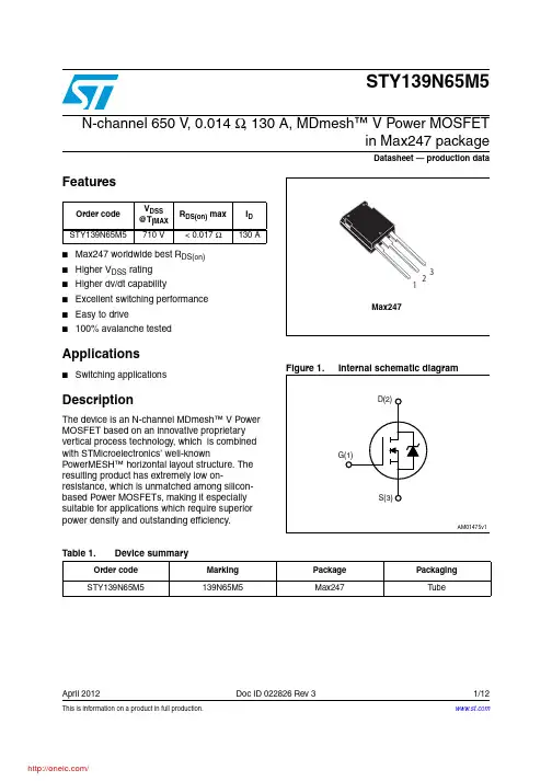
This is information on a product in full production.April 2012Doc ID 022826 Rev 31/12STY139N65M5N-channel 650 V , 0.014 Ω, 130 A, MDmesh™ V Power MOSFETin Max247 packageDatasheet — production dataFeatures■Max247 worldwide best R DS(on)■Higher V DSS rating ■Higher dv/dt capability■Excellent switching performance ■Easy to drive■100% avalanche testedApplications■Switching applicationsDescriptionThe device is an N-channel MDmesh™ V Power MOSFET based on an innovative proprietary vertical process technology, which is combined with STMicroelectronics’ well-knownPowerMESH™ horizontal layout structure. The resulting product has extremely low on-resistance, which is unmatched among silicon-based Power MOSFETs, making it especially suitable for applications which require superior power density and outstanding efficiency.Order code V DSS @T jMAX R DS(on) max I D STY139N65M5710 V< 0.017 Ω130 ATable 1.Device summaryOrder code Marking Package Packaging STY139N65M5139N65M5Max247TubeContents STY139N65M5Contents1Electrical ratings . . . . . . . . . . . . . . . . . . . . . . . . . . . . . . . . . . . . . . . . . . . . 32Electrical characteristics . . . . . . . . . . . . . . . . . . . . . . . . . . . . . . . . . . . . . 42.1Electrical characteristics (curves) . . . . . . . . . . . . . . . . . . . . . . . . . . . . 6 3Test circuits . . . . . . . . . . . . . . . . . . . . . . . . . . . . . . . . . . . . . . . . . . . . . . 8 4Package mechanical data . . . . . . . . . . . . . . . . . . . . . . . . . . . . . . . . . . . . . 9 5Revision history . . . . . . . . . . . . . . . . . . . . . . . . . . . . . . . . . . . . . . . . . . . 122/12Doc ID 022826 Rev 3STY139N65M5Electrical ratingsDoc ID 022826 Rev 33/121 Electrical ratingsTable 2.Absolute maximum ratingsSymbol ParameterValue Unit V GS Gate- source voltage± 25V I D Drain current (continuous) at T C = 25 °C 130A I D Drain current (continuous) at T C = 100 °C 78A I DM (1)1.Pulse width limited by safe operating area.Drain current (pulsed)520A P TOT Total dissipation at T C = 25 °C625W I AR Max current during repetitive or single pulse avalanche(pulse width limited by T JMAX )15A E AS Single pulse avalanche energy(starting T j = 25°C, I D = I AR , V DD = 50V)2000mJ dv/dt (2)2.I SD ≤ 130 A, di/dt = 400 A/µs, V DD = 400 V, peak V DS < V (BR)DSS.Peak diode recovery voltage slope 15V/ns T stg Storage temperature- 55 to 150°C T jMax. operating junction temperature150°CTable 3.Thermal dataSymbolParameterValue Unit R thj-case Thermal resistance junction-case max 0.2°C/W R thj-amb Thermal resistance junction-ambient max 30°C/W T lMaximum lead temperature for soldering purpose300°CElectrical characteristics STY139N65M54/12Doc ID 022826 Rev 32 Electrical characteristics(T C = 25 °C unless otherwise specified)Table 4.On /off statesSymbol Parameter Test conditionsMin.Typ.Max.Unit V (BR)DSS Drain-sourcebreakdown voltageI D = 1 mA, V GS = 0650V I DSS Zero gate voltage drain current (V GS = 0)V DS = 650 VV DS = 650 V , T C =125 °C 10100µA µA I GSS Gate-body leakage current (V DS = 0)V GS = ± 25 V±100nA V GS(th)Gate threshold voltage V DS = V GS , I D = 250 µA 345V R DS(on)Static drain-source onresistanceV GS = 10 V , I D = 65 A0.0140.017ΩTable 5.DynamicSymbol Parameter Test conditionsMin.Typ.Max.Unit C iss C oss C rss Input capacitance Output capacitance Reverse transfer capacitance V DS = 100 V , f = 1 MHz, V GS = 0-156003659-pF pF pFC o(tr)(1)1.C o(tr) is a constant capacitance value that gives the same charging time as C oss while V DS is rising from 0to 80% V DSS .Equivalentcapacitance time relatedV GS = 0, V DS = 0 to 520 V-1559-pFC o(er)(2)2.C o(er) is a constant capacitance value that gives the same stored energy as C oss while V DS is rising from 0to 80% V DSS .Equivalentcapacitance energy related V GS = 0, V DS = 0 to 520 V -360-pFR GIntrinsic gate resistancef = 1 MHz open drain - 1.2-ΩQg Q gs Q gdT otal gate charge Gate-source charge Gate-drain chargeV DD = 520 V , I D = 65 A,V GS = 10 V (see Figure 15)-36388164-nC nC nCSTY139N65M5Electrical characteristicsDoc ID 022826 Rev 35/12Table 6.Switching timesSymbol ParameterTest conditions Min.Typ.Max.Unitt d(v)t r(v)t f(i)t c(off)Voltage delay time Voltage rise time Current fall time Crossing timeV DD = 400 V , I D = 80 A, R G = 4.7 Ω, V GS = 10 V (see Figure 16)(see Figure 19)-295563784-ns ns ns nsTable 7.Source drain diodeSymbol ParameterTest conditionsMin.Typ.Max.Unit I SD I SDM (1)1.Pulse width limited by safe operating area.Source-drain currentSource-drain current (pulsed)-130520A A V SD (2)2.Pulsed: pulse duration = 300 µs, duty cycle 1.5%Forward on voltage I SD = 130 A, V GS = 0- 1.5V t rr Q rr I RRM Reverse recovery time Reverse recovery charge Reverse recovery current I SD = 130 A, di/dt = 100 A/µs V DD = 100 V (see Figure 16)-5701553ns µC A t rr Q rr I RRMReverse recovery time Reverse recovery charge Reverse recovery currentI SD = 130 A, di/dt = 100 A/µs V DD = 100 V , T j = 150 °C (see Figure 16)-7202468ns µC AElectrical characteristics STY139N65M5 2.1 Electrical characteristics (curves)6/12Doc ID 022826 Rev 3STY139N65M5Electrical characteristicsDoc ID 022826 Rev 37/12Figure 10.Normalized gate threshold voltageFigure 11.Normalized on resistance vsFigure 12.Output capacitance stored energyFigure 13.Switching losses vs gate resistance(1)1.Eon including reverse recovery of a SiC diode.Test circuits STY139N65M58/12Doc ID 022826 Rev 33 Test circuitsFigure 14.Switching times test circuit forFigure 15.Gate charge test circuitFigure 16.Test circuit for inductive loadFigure 17.Unclamped inductive load testFigure 18.Unclamped inductive waveformFigure 19.Switching time waveformSTY139N65M5Package mechanical data 4 Package mechanical dataIn order to meet environmental requirements, ST offers these devices in different grades ofECOP ACK® packages, depending on their level of environmental compliance. ECOPACK®specifications, grade definitions and product status are available at: .ECOP ACK® is an ST trademark.Table 8.Max247 mechanical datammDim.Min.Typ.Max.A 4.70 5.30A1 2.20 2.60b 1.00 1.40b1 2.00 2.40b2 3.00 3.40c0.400.80D19.7020.30e 5.35 5.55E15.3015.90L14.2015.20L1 3.70 4.30Doc ID 022826 Rev 39/12Package mechanical data STY139N65M510/12Doc ID 022826 Rev 3分销商库存信息: STMSTY139N65M5。