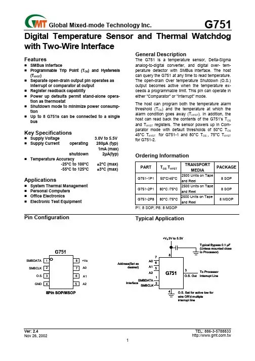
with Two-Wire Interface FeaturesSMBus interfaceProgrammable Trip Point (T OS) and Hysteresis (T HYST)Separate open-drain output pin operates as interrupt or comparator at outputRegister readback capabilityPower up defaults permit stand-alone opera-tion as thermostatShutdown mode to minimize power consump-tionUp to 8 G751s can be connected to a single busKey SpecificationsSupply Voltage 3.0V to 5.5V Supply Current operating 280µA (typ)1mA (max)shutdown 2µA(typ) Temperature Accuracy-25°C to 100°C ±2°C (max)-55°C to 125°C ±3°C (max) ApplicationsSystem Thermal ManagementPersonal ComputersOffice ElectronicsElectronic Test Equipment General DescriptionThe G751 is a temperature sensor, Delta-Sigma analog-to-digital converter, and digital over- tem-perature detector with SMBus interface. The host can query the G751 at any time to read temperature. The open-drain Over temperature Shutdown (O.S.) output becomes active when the temperature ex-ceeds a programmable limit. This pin can operate in either “Comparator” or “Interrupt” mode.The host can program both the temperature alarm threshold (T OS) and the temperature at which the alarm condition goes away (T HYST). In addition, the host can read back the contents of the G751’s T OS and T HYST registers. The sensor powers up in Com-parator mode with default thresholds of 50°C T OS 45°C T HYST. for G751-1 and 80°C T OS , 75°C T HYST for G751-2.Ordering InformationPART T OS T HYSTTRANSPORTMEDIAPACKAGE G751-1P1 50°C/45°C2500 Units on Tapeand Reel8 SOPG751-2P1 80°C/75°C2500 Units on Tapeand Reel8 SOPG751-2P8 80°C/75°C2500 Units on Tapeand Reel8 MSOP P1: 8 SOP; P8: 8 MSOPTypical ApplicationSMBDATA8Pin SOP/MSOP +Vs A0 A1 A2SMBCLKGND Address(Set asInterfaceinterrupt line desired)A0A1A2Supply Voltage………….…………………-0.3V to 6.5V Voltage at any Pin……………….…-0.3V to +Vs +0.3V Input Current at any Pin…………………………….5mA Package Input Current…………………………….20mA O.S. Output Sink Current………………………….10mA O.S. Output Voltage…………………….…………..6.5V Storage Temperature…………………-65°C to +150°C Soldering Information, Lead TemperatureSOP PackageVapor Phase (60 seconds)……………………….215°C Infrared (15 seconds)……………………………..220°C ESD SusceptibilityHuman Body Model (2000V)Machine Model……………………………………...200V Specified Temperature Range…………….T MIN to T MAX-55°Cto+125°C Supply Voltage Range (+Vs)…………..+3.0V to +5.5VTemperature-to-Digital Converter CharacteristicsUnless otherwise noted, these specifications apply for +Vs=+3.3v Vdc. Boldface limits apply for T A=T J=T MIN toT MAX; all other limits T A=T J= +25°C, unless otherwise noted.PARAMETER CONDITIONSTYPICALLIMITSUNITSAccuracy TA=-25°C to +100°CTA=-55°C to +125°C±2.0±3.0 °C (max)Resolution9BitsTemperature Conversion Time 100 MsQuiescent Current SMBus InactiveSMBus ActiveShutdown Mode0.2511.0MamA (max)µAO.S. Output Saturation Voltage I OUT = 4.0mA 0.8 V (max)O.S. Delay 16Conversions (min)Conversions (max)T OS Default Temperature G751-1/G751-2 50/80 °C T HYST Default Temperature G751-1/G751-2 45/75 °CBlock DiagramA0SMBDATAA1A2SMBCLKDigital DC CharacteristicsUnless otherwise noted, these specifications apply for +Vs=+3.3 Vdc. Boldface limits apply for T A =T J =T MIN to T MAX ; all other limits T A =T J =+25°C, unless otherwise noted. SYMBOL PARAMETER CONDITIONS TYPICAL LIMITS UNITSV IN (1) Logical “1” Input Voltage +Vs × 0.7 +Vs + 0.5 V (min) V (max) V IN (0) Logical “0” Input Voltage-0.3 +Vs ×0.3V (min) V (max) I IN (1) Logical “1”Intput Current V IN =5V 0.005 1.0 µA I IN (0) Logical “0”Intput Current V IN =0V -0.005 -1.0µA C IN All Digital Inputs20 PF I OH High Level Output Current V OH =5V 100 µA (max) V OL Low Level Output Voltage I OL =3ma 0.4 V (max) t OFOutput Fall TimeC L =400pF,I O =3ma 250ns (max)SMBus Digital Switching CharacteristicsUnless otherwise noted, these specifications apply for +Vs = +3.3 Vdc and C L (load capacitance) on output lines = 80pF unless otherwise specified. Boldface limits apply for T A = T J = T MIN to T MAX ; all other limits T A = T J = +25°C, unless otherwise noted.The switching characteristics of the G751 fully meet or exceed the published specifications of the SMBus. The following parameters are the timing relationships between SMBCLK and SMBDATA signals related to the G751. They are not the SMBus specifications.SYMBOL PARAMETER CONDITIONS TYPICAL LIMITSUNITSt 1 SMBCLK (Clock) Period2.5 µs (min) t 2 Data in Set-Up Time to SMBCLK High 100 ns (min) t 3 Data Out Stable after SMBCLK Low0 ns (min) t 4 SMBDATA Low Set-Up Time to SMBCLK Low (Start Condition) 100 ns (min) t 5SMBDATA High Hold Time after SMBCLK High (Stop Condition)100ns (min)Pin DescriptionPIN LABELFUNCTIONTYPICAL CONNECTION1 SMBDATA SMBus Serial Bi-Directional Data Line From Controller2 SMBCLK SMBus Clock Input From Controller3 O.S. Overtemperature Shutdown Open Drain Output Pull Up Resistor, Controller Interrupt Line4 GND Power Supply GroundGround5,6,7 A0-A2 User-Set SMBus Address Inputs Ground (Low, “0”) or +Vs (High, “1”) 8 +Vs Positive Supply Voltage InputDC Voltage from 3V to 5.5VLogic Electrical CharacteristicsSMBDATASMBDATA SMBCLKData inData outTemperature-to-Digital Transfer Function (Non-linear scale for clarity)Functional DescriptionThe G751 temperature sensor incorporates a band-gap type temperature sensor and 9-bit ADC (Delta-Sigma Analog- to-Digital Converter). The temperature data output of the G751 is available at all times via the SMBus. If a conversion is in pro-gress, it will be stopped and restarted after the read.A digital comparator is also incorporated that com-pares a series of readings, the number of which is user-selectable, to user-programmable setpoint and hysteresis values. The comparator trips the O.S. output line, which is programmable for mode and polarity.O.S. Output, T OS and T HYST LimitsIn Comparator mode the O.S. Output behaves like a thermostat. The output becomes active when tem-perature exceeds the T OS limit, and leaves the active state when the temperature drops below the T HYST limit. In this mode the O.S. output can be used to turn a cooling fan on, initiate an emergency system shutdown, or reduce system clock speed. Shutdown mode does not reset O.S. state in a comparator mode.In interrupt mode exceeding T OS also makes O.S. active but O.S. will remain active indefinitely until reset by reading any register via the SMBus inter-face. Once O.S. has been activated by crossing T OS, then reset, it can activated again only by Tempera-ture going below T HYST. Again, it will remain active indefinitely until being reset by a read. Placing the G751 in shutdown mode also resets the O.S. output. Default ModesG751 always powers up in a known state. G751 power up default conditions are:1. Comparator mode2. T OS set to 50°C for G751-1, to 80°C for G751-23. T HYST set to 45°C for G751-1, to 75°C for G751-24. O.S. active low5. Pointer set to “00”; Temperature RegisterWith these operating conditions G751 can act as a stand-alone thermostat with the above temperature settings. Connection to an SMBus is not required. SMBus InterfaceThe G751 operates as a slave on the SMBus, so the SMBCLK line is an input (no clock is generated bythe G751) and the SMBDATA line is a bi-directional serial data path. According to SMBus specifications,the G751 has a 7-bit slave address. The four most significant bits of the slave address are hard wired inside the G751 and are “1001”. The three least sig-nificant bits of the address are assigned to pinsA2-A0, and are set by connecting these pins to ground for a low, (0); or to +Vs for a high, (1). Therefore, the complete slave address is:1 0 0 1 A2 A1 A0 MSB LSBFigure1 O.S. Output Temperature Response Diagram Temperature Data FormatTemperature data can be read from the Temperature, T OS Set Point, and T HYST Set Point registers; and written to the T OS Set Point, and T HYST Set Point reg-isters. Temperature data is representedby a 9-bit, two’s complement word with an LSB (Least Significant Bit) equal to 0.5°C:DIGITAL OUTPUTTEMPERATUREBINARY HEX+125°C 0 1111 1010 0FAh +25°C 0 0011 0010 032h +0.5°C 0 0000 0001 001h 0°C 0 0000 0000 000h -0.5°C 1 1111 1111 1FFh -25°C 1 1100 1110 1CEh -55°C 1 1001 0010 192hShutdown ModeShutdown mode is enabled by setting the shutdown bit in the Configuration register via the SMBus. Shut-down mode reduces power supply current to 1 µA typical. In interrupt mode O.S. is reset if previously set and is undefined in Compatator mode during shutdown. The SMBus interface remains active. Ac-tivity on the clock and data lines of the SMBus may slightly increase shutdown mode quiescent current. T OS , T HYST , and Configuration registers can be read from and written to in shutdown mode.Fault QueueA fault queue of up to 6 faults is provided to prevent false tripping of O.S. when the G751 is used in noisy environments. The number of faults set in the queue must occur consecutively to set the O.S. output. Comparator/Interrupt ModeAs indicated in the O.S. Output Temperature Re-sponse Diagram, Figure 1, the events that trigger O.S. are identical for either Comparator or Interrupt mode. The most important difference is that in Inter-rupt mode the O.S. will remain set indefinitely once it has been set. To reset O.S. while in Interrupt mode, perform a read from any register in the G751. O.S. OutputThe O.S. output is an open-drain output and does not have an internal pull-up. A ”high” level will not be observed on this pin until pull-up current is provided from some external source, typically a pull-up resis-tor. Choice of resistor value depends on many sys-tem factors but, in general, the pull-up resistor should be as large as possible. This will minimize any errors due to internal heating of the G751. The maximum resistance of the pull up, based on G751 specification for High Level Output Current, to pro-vide a 2V high level, is 30k Ω.O.S. PolarityThe O.S. output can be programmed via the con-figuration register to be either active low (default mode), or active high. In active low mode the O.S. output goes low when triggered exactly as shown on the O.S. Output Temperature Response Diagram, Figure 1. Active high simply inverts the polarity of the O.S. output.T T O ST H Y S TO .S .(C o m p a r a t o r M o d e )O .S .(I n t e r r u p t M o d e )e m p e r a t u S h o w nf o r O .S . s e t f o r a c t i v e l o w .*r e a d a n y r e g i s t e r o r p l a c e d i n s h u t d o w nThere are four data registers in the G751, selected by the Pointer register. At power-up the Pointer is set to “00”; the location for the Temperature Register. The Pointer register latches whatever the last loca-tion it was set to. In Interrupt Mode, a read from the G751, or placing the device in shutdown mode, re-sets the O.S. output. All registers are read and write, except the Temperature register which is read only. A write to the G751 will always include the address byte and the Pointer byte. A write to the Configura-tion register requires one data byte, and the T OS and T HYST registers require two data bytes.Reading the G751 can take place either of two ways: If the location latched in the Pointer is correct (most of the time it is expected that the Pointer will point to Temperature register because it will be the data most frequently read from the G751), then the read can simply consist of an address byte, followed by retrieving the corresponding number of data bytes. If the Pointer needs to be set, than an address byte, pointer byte, repeat start, and another address byte will accomplish a read.The first data byte is the most significant byte with most signification bit first, permitting only as much data as necessary to be read to determine tempera-ture condition. For instance, if the first four bits of the temperature data indicates an overtemperature con-dition, the host processor could immediately take action to remedy the excessive temperatures. At the end of a read, the G751 can accept either Acknowl-edge or No Acknowledge from the Master (No Ac-knowledge is typically used as a signal for the salve that the Master has read its last byte).An inadvertent 8-bit read from a 16-bit register, with the D7 bit low, can cause the G751 to stop in a state where the SDA line is held low as shown in Figure 2. This can prevent any further bus communication until at least 9 additional clock cycles have occurred. Al-ternatively, the master can issue clock cycles until SDA goes high, at which time issuing a “Stop” condi-tion will reset the G751.Figure 2. Inadvertent 8-Bit Read from 16-Bit Register where D7 is ZeroMaster but G751 locks SMBDATA low Master detects the errorSMBCLKSMBDATAIntended Stop byof its ways(Selects which registers will be read from or written to):P7 P6 P5 P4 P3 P2 P1 P00 0 0 0 0 0 RegisterSelectP0-P1 :Register Select:P1 P0 REGISTER0 0 Temperature (Read only) (Power-up default)Configuration(Read/Write)0 1T HYST (Read/Write)1 0T OS (Read/Write)1 1P2-P7 :Must be kept zero.Temperature Register(Read Only):D15 D14 D13 D12 D11 D10 D9 D8 D7 D6 D5 D4 D3 D2 D1 D0MSB Bit 7 Bit 6 Bit 5 Bit 4 Bit 3 Bit 2 Bit 1 LSB X X X X X X XD0-D6 :UndefinedD7-D15 :Temperature Data. One LSB = 0.5°C. Two’s complement format.Configuration Register(Read/Write):D7 D6 D5 D4 D3 D2 D1 D0Cmp/IntShutdownPolarity0 0 0 FaultO.S.QueuePower up default is with all bits “0” (zero).D0 :Shutdown : When set to 1 the G751 goes to low power shutdown mode.D1 :Comparator / Interrupt mode : 0 is Comparator mode, 1 is Interrupt mode.D2 :O.S. Polarity : 0 is active low, 1 is active high. O.S. is an open-drain output under all conditions.D3-D4 :Fault Queue : Number of faults necessary to detect before setting O.S. output to avoid false tripping dueto noise :OFFAULTS D4 D3NUMBER0 0 1 (Power-up default)0 1 21 0 41 1 6D5-D7 :These bits are used for production testing and must be kept zero for normal operation.T HYST and T OS Register(Read/Write):D15 D14 D13 D12 D11 D10 D9 D8 D7 D6 D5 D4 D3 D2 D1 D0MSB Bit 7 Bit 6 Bit 5 Bit 4 Bit 3 Bit 2 Bit 1 LSB X X X X X X XD0-D6 :UndefinedD7-D15 :T HYST Or T OS Trip Temperature Data. Power up default is T OS = 50°C /80°C for G751-1/G751-2, T HYST =45°C /75°C for G751-1/G751-2.StartG751AckStartG751Master NoCondRepeat Ack Ack No Cond StartG751G751CondbyMasterAddress Byte AckbyPointer BytebyG751byMasterAddress Byte AckbyMost Significant Data ByteAckbyAckbyMasterStopbyMasterLeast Significant Data ByteStartby Master Address BytebyG751Most Significant Data BytebyMasterAckbyMasterStopbyMasterLeast Significant Data BytebyMasterAddress Byte AckbyPointer ByteAckbyStopbyMasterS n S A A A S A A A C t o p C o d b y M a s t e rt a r t b y M a s t e rA d d r e s sB y t ec k b y G 751P o i n t e r B y t e c k b y M a s t e r N o A c k b y M a s t e r A d r e s s B y t e919199R e p e a t S t a r t b y M a s t e r D a t a B y t ec k b y G 751t a r t b y M a s t e rA d d r e s sB y t ec k b y G 751P o i n t e r B y t e c k b y M a s t e r c k b y G 751S t o p o n d b y M a s t e rC o n f i g u r a t i o n B y t et o p o n d b y s t e r1(a ) T y p i c a l P o i n t e r S e t f o l l o w e d b y I m m e d i a t e R e a d f r o m C o n f i g u r a t i o n R e g i s t e r(b ) C o n f i g u r a t i o n R e g i s t e r W r i t e(c ) T O S a n d T H Y S T W r i t e8 Pin SOP PackageNote:1. Package body sizes exclude mold flash and gate burrs2. Dimension L is measured in gage plane3. Tolerance 0.10mm unless otherwise specified4. Controlling dimension is millimeter converted inch dimensions are not necessarily exact.DIMENSION IN MM DIMENSION IN INCHSYMBOLMIN. NOM. MAX. MIN. NOM. MAX.A 1.35 1.60 1.75 0.053 0.063 0.069 A1 0.10 ----- 0.25 0.004 ----- 0.010 A2 ----- 1.45 ----- ----- 0.057 -----B 0.33 ----- 0.51 0.013 ----- 0.020C 0.19 ----- 0.25 0.007 ----- 0.010D 4.80 ----- 5.00 0.189----- 0.197 E 3.80 ----- 4.00 0.150 ----- 0.157 e ----- 1.27 ----- ----- 0.050 ----- H 5.80 ----- 6.20 0.228 ----- 0.244 L 0.40 ----- 1.27 0.016 ----- 0.050 y ----- ----- 0.10 ----- ----- 0.004 θ 0º ----- 8º 0º ----- 8ºVer: 2.4Nov 26, 2002TEL: 886-3-5788833 118 Pin MSOP PackageDIMENSION IN MM DIMENSION IN INCHSYMBOLMIN. NOM. MAX. MIN. NOM. MAX.A ----- ----- 1.10 ----- ----- 0.043 A1 0.05 ----- 0.15 0.002 ----- 0.006A2 0.81 0.86 0.91 0.032 0.034 0.036 b 0.25 ----- 0.40 0.008----- 0.012b1 0.25 0.30 0.35 0.010 0.012 0.014 c 0.13 ----- 0.23 0.005 0.009 c1 0.13 0.15 0.18 0.005 0.006 0.007 D 2.90 3.00 3.10 0.114 0.118 0.122 E1 2.90 3.00 3.10 0.1140.118 0.122 e 0.65 BSC 0.026 BSC E 4.90 BSC 0.193 BSC L 0.445 0.55 0.648 0.0175 0.0217 0.0255 θ1 0° ----- 6° 0° ----- 6° θ2 12 REF 12 REF θ3 12 REF 12 REF R 0.09 ----- ----- 0.004 ----- ----- R1 0.09 ----- ----- 0.004 ----- ----- JEDEC MO-187AATaping SpecificationGMT Inc. does not assume any responsibility for use of any circuitry described, no circuit patent licenses are implied and GMT Inc. reserves the right at any time without notice to change said circuitry and specifications.Typical SOP/MSOP Package OrientationC b1E18E1DETAIL “A”Leb DA2AA1SEATING PLANEbWITH PLATINGBASE METALc1cθ1GAUGE PLANE0.25RR1Lθ3θ2元器件交易网。