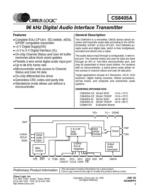
Preliminary Product InformationThis document contains information for a new product.Cirrus Logic reserves the right to modify this product without notice.Copyright ©Cirrus Logic,Inc.2002Cirrus Logic,Inc.P.O.Box 17847,Austin,Texas 78760CS8405A96kHz Digital Audio Interface TransmitterFeaturesCompleteEIAJ CP1201,IEC-60958,AES3,S/PDIF compatible transmitter +5V Digital Supply(VD)+3V to 5V Digital Interface (VL)On-chip Channel Status and User bit buffer memories allow block sized updatesFlexible 3-wire serial digital audio input port Up to 96kHz frame rateMicrocontroller write access to Channel Status and User bit dataOn-chip differential line driverGenerates CRC codes and parity bits Standalone mode allows use without a microcontrollerGeneral DescriptionThe CS8405A is a monolithic CMOS device which en-codes and transmits audio data according to the AES3,IEC60958,S/PDIF,or EIAJ CP1201.The CS8405A ac-cepts audio and digital data,which is then multiplexed,encoded and driven onto a cable.The audio data is input through a configurable,3-wire in-put port.The channel status and user bit data are input through an SPI or Two-Wire microcontroller port,and may be assembled in block sized buffers.For systems with no microcontroller,a stand alone mode allows di-rect access to channel status and user bit data pins.Target applications include A/V Receivers,CD-R,DVD receivers,digital mixing consoles,effects processors,set-top boxes,and computer and automotive audio systems.ORDERING INFORMATIONCS8405A-CS 28-pin SOIC -10to +70°C CS8405A-CZ 28-pin TSSOP -10to +70°C CS8405A-IS 28-pin SOIC -40to +85°C CS8405A-IZ 28-pin TSSOP -40to +85°C CDB8415AEvaluation BoardJUN ‘02TABLE OF CONTENTS1.CHARACTERISTICS AND SPECIFICATIONS (4)POWER AND THERMAL CHARACTERISTICS (4)ABSOLUTE MAXIMUM RATINGS (4)DIGITAL CHARACTERISTICS (5)SWITCHING CHARACTERISTICS (5)SWITCHING CHARACTERISTICS-SERIAL AUDIO PORTS (6)SWITCHING CHARACTERISTICS-CONTROL PORT-SPI MODE (7)SWITCHING CHARACTERISTICS-CONTROL PORT-TWO-WIRE MODE (8)2.TYPICAL CONNECTION DIAGRAM (9)3.GENERAL DESCRIPTION (10)3.1AES3and S/PDIF Standards Documents (10)4.THREE-WIRE SERIAL INPUT AUDIO PORT (10)5.AES3TRANSMITTER (12)5.1Transmitted Frame and Channel Status Boundary Timing (12)5.2TXN and TXP Drivers (12)5.3Mono Mode Operation (12)6.CONTROL PORT DESCRIPTION AND TIMING (14)6.1SPI Mode (14)6.2Two-Wire Mode (15)6.3Interrupts (15)7.CONTROL PORT REGISTER SUMMARY (16)7.1Memory Address Pointer(MAP) (16)8.CONTROL PORT REGISTER BIT DEFINITIONS (17)8.1Control1(1h) (17)8.2Control2(2h) (18)8.3Data Flow Control(3h) (18)8.4Clock Source Control(4h) (19)8.5Serial Audio Input Port Data Format(5h) (19)8.6Interrupt1Status(7h)(Read Only) (20)8.7Interrupt2Status(8h)(Read Only) (21)8.8Interrupt1Mask(9h) (21)Contacting Cirrus Logic SupportFor a complete listing of Direct Sales,Distributor,and Sales Representative contacts,visit the Cirrus Logic web site at: /corporate/contacts/sales.cfmIMPORTANT NOTICE"Preliminary"product information describes products that are in production,but for which full characterization data is not yet available."Advance"product infor-mation describes products that are in development and subject to development changes.Cirrus Logic,Inc.and its subsidiaries("Cirrus")believe that the infor-mation contained in this document is accurate and reliable.However,the information is subject to change without notice and is provided"AS IS"without warranty of any kind(express or implied).Customers are advised to obtain the latest version of relevant information to verify,before placing orders,that information being relied on is current and complete.All products are sold subject to the terms and conditions of sale supplied at the time of order acknowledgment,including those pertaining to warranty,patent infringement,and limitation of liability.No responsibility is assumed by Cirrus for the use of this information,including use of this information as the basis for manufacture or sale of any items,or for infringement of patents or other rights of third parties.This document is the property of Cirrus and by furnishing this information,Cirrus grants no license,express or implied under any patents,mask work rights,copyrights,trademarks,trade secrets or other intellectual property rights.Cirrus owns the copyrights of the information contained herein and gives consent for copies to be made of the information only for use within your organization with respect to Cirrus integrated circuits or other parts of Cirrus.This consent does not extend to other copying such as copying for general distribution,advertising or promotional purposes,or for creating any work for resale.An export permit needs to be obtained from the competent authorities of the Japanese Government if any of the products or technologies described in this ma-terial and controlled under the"Foreign Exchange and Foreign Trade Law"is to be exported or taken out of Japan.An export license and/or quota needs to be obtained from the competent authorities of the Chinese Government if any of the products or technologies described in this material is subject to the PRC Foreign Trade Law and is to be exported or taken out of the PRC.CERTAIN APPLICATIONS USING SEMICONDUCTOR PRODUCTS MAY INVOLVE POTENTIAL RISKS OF DEATH,PERSONAL INJURY,OR SEVERE PROPERTY OR ENVIRONMENTAL DAMAGE("CRITICAL APPLICATIONS").CIRRUS PRODUCTS ARE NOT DESIGNED,AUTHORIZED,OR WARRANT-ED TO BE SUITABLE FOR USE IN LIFE-SUPPORT DEVICES OR SYSTEMS OR OTHER CRITICAL APPLICATIONS.INCLUSION OF CIRRUS PRODUCTS IN SUCH APPLICATIONS IS UNDERSTOOD TO BE FULLY AT THE CUSTOMER'S RISK.Cirrus Logic,Cirrus,and the Cirrus Logic logo designs are trademarks of Cirrus Logic,Inc.All other brand and product names in this document may be trade-marks or service marks of their respective owners.8.9Interrupt1Mode MSB(Ah)and Interrupt1Mode LSB(Bh) (21)8.10Interrupt2Mask(Ch) (21)8.11Interrupt2Mode MSB(Dh)and Interrupt Mode2LSB(Eh) (22)8.12Channel Status Data Buffer Control(12h) (22)8.13User Data Buffer Control(13h) (23)8.14Channel Status bit or User bit Data Buffer(20h-37h) (23)8.15CS8405A I.D.and Version Register(7Fh)(Read Only) (23)9.PIN DESCRIPTION-SOFTWARE MODE (24)10.HARDWARE MODE (26)10.1Channel Status,User and Validity Data (26)10.2Serial Audio Port Formats (26)11.PIN DESCRIPTION-HARDWARE MODE (28)12.APPLICATIONS (30)12.1Reset,Power Down and Start-up (30)12.2ID Code and Revision Code (30)12.3Power Supply,Grounding,and PCB layout (30)12.4Synchronization of Multiple CS8405As (30)12.4ORDERING INFORMATION (30)13.PACKAGE DIMENSIONS (31)14.APPENDIX A:EXTERNAL AES3/SPDIF/IEC60958TRANSMITTER COMPONENTS (33)14.1AES3Transmitter External Components (33)14.2Isolating Transformer Requirements (33)15.APPENDIX B:CHANNEL STATUS AND USER DATA BUFFER MANAGEMENT (34)15.1AES3Channel Status(C)Bit Management (34)15.1.1Accessing the E buffer (34)15.1.2Serial Copy Management System(SCMS) (35)15.1.3Channel Status Data E Buffer Access (35)15.2AES3User(U)Bit Management (35)15.2.1Mode1:Transmit All Zeros (35)15.2.2Mode2:Block Mode (35)LIST OF FIGURESFigure1.Audio Port Master Mode Timing (6)Figure2.Audio Port Slave Mode and Data Input Timing (6)Figure3.SPI Mode timing (7)Figure4.Two-Wire Mode timing (8)Figure5.Recommended Connection Diagram for Software Mode (9)Figure6.Serial Audio Input Example Formats (11)Figure7.AES3Transmitter Timing for C,U and V pin input data (13)Figure8.Control Port Timing in SPI Mode (14)Figure9.Control Port Timing in Two-Wire Mode (15)Figure10.Hardware Mode (26)Figure11.Professional Output Circuit (33)Figure12.Consumer Output Circuit (33)Figure13.TTL/CMOS Output Circuit (33)Figure14.Channel Status Data Buffer Structure (34)Figure15.Flowchart for Writing the E Buffer (34)1.CHARACTERISTICS AND SPECIFICATIONSPOWER AND THERMAL CHARACTERISTICS (DGND =0V,all voltages with respect toground)Notes: 1.-CS’and ‘-CZ’parts are specified to operate over -10°C to 70°C but are tested at 25°C only.2.‘-IS’and ‘-IZ’parts are tested over the full -40°C to 85°C temperature range.ABSOLUTE MAXIMUM RATINGS(DGND =0V,all voltages with respect to ground)Notes: 3.Transient currents of up to 100mA will not cause SCR latch-up.ParameterSymbol Min Typ Max Units Power Supply VoltageVD+VL+4.52.855.0- 5.55.5V V Supply Current at 48kHz frame rateVD+VL+=3V VL+=5V --- 6.330.146.5---mA mA mA Supply Current at 96kHz frame rateVD+VL+=3V VL+=5V--- 6.644.876.6---mA mA mA Supply Current in power downReset high,VD+Reset high,VL+=3V Reset high,VL+=5V---206060---µA µA µA Ambient Operating Temperature:CS8405-CS &-CZ (Note 1)CS8405-IS &-IZ (Note 2)T A -10-40257085°CParameterSymbol Min Max Units Power Supply VoltageVD/VL+- 6.0V Input Current,Any Pin Except Supply (Note 3)I in -±10mA Input VoltageV in -0.3(VL+)+0.3V Ambient Operating Temperature (power applied)T A -55125°C Storage T emperatureT stg-65150°CDIGITAL CHARACTERISTICS(T A=25°C for suffixes‘CS’&’CZ’,T A=-40to85°C for‘IS’&‘IZ’;VD+=5V±10%,VL+=3/5V±5/10%)Parameter Symbol Min Typ Max Units High-Level Input Voltage V IH 2.0-(VL+)+0.3V Low-Level Input Voltage(Note4)V IL-0.3-0.4/0.8V Low-Level Output Voltage,(Io=-3.2mA),except TXP,TXN V OL--0.4V High-Level Output Voltage,(Io=3.2mA),except TXP,TXN V OH(VL+)-1--V Input Leakage Current I in-±1±10µA Output High Voltage,TXP,TXN(I OH=14mA)(VL+)-0.7(VL+)-0.4-V Output Low Voltage,TXP,TXN(I OL=14mA)-0.40.7VNotes: 4.At5V mode,V IL=0.8V(Max),at3V mode,V IL=0.4V(Max).SWITCHING CHARACTERISTICS(T A=25°C for suffixes‘CS’&’CZ’,T A=-40to85°C for‘IS’&‘IZ’;VD+=5V±10%,VL+=3/5V±5/10%,Inputs: Logic0=0V,Logic1=VL+;C L=20pF)Parameter Symbol Min Typ Max Units RST pin Low Pulse Width200--µs OMCK Frequency for OMCK=512*Fs 4.1-55.3MHz OMCK Low and High Width for OMCK=512*Fs7.2--ns OMCK Frequency for OMCK=384*Fs 3.1-41.5MHz OMCK Low and High Width for OMCK=384*Fs9.6--ns OMCK Frequency for OMCK=256*Fs 2.0-27.7MHz OMCK Low and High Width for OMCK=256*Fs14.4--ns Frame Rate8.0-108.0kHz AES3Transmitter Output Jitter--1nsSWITCHING CHARACTERISTICS -SERIAL AUDIO PORTS(T A =25°C for suffixes ‘CS’&’CZ’,T A =-40to 85°C for ‘IS’&‘IZ’;VD+=5V±10%,VL+=3/5V ±5/10%,Inputs:Logic 0=0V,Logic 1=VL+;C L =20pF)Notes: 5.The active edge of ISCLK is programmable.6.The polarity of ILRCK is programmable.7.No more than 128SCLK per frame.8.This delay is to prevent the previous ISCLK edge from being interpreted as the first one after ILRCK haschanged.9.This setup time ensures that this ISCLK edge is interpreted as the first one after ILRCK has changed.ParameterSymbol Min Typ Max Units SDIN Setup Time Before ISCLK Active Edge (Note 5)t ds 20--ns SDIN Hold Time After ISCLK Active Edge(Note 5)t dh20--nsMaster ModeOMCK to ISCLK active edge delay (Note 5)t smd 0-10ns OMCK to ILRCK delay (Note 6)t lmd0-10ns ISCLK and ILRCK Duty Cycle -50-%Slave Mode ISCLK Period(Note 7)t sckw 36--ns ISCLK Input Low Width t sckl 14--ns ISCLK Input High Widtht sckh 14--ns ISCLK Active Edge to ILRCK Edge(Note 5,6,8)t lrckd 20--ns ILRCK Edge Setup Before ISCLK Active Edge(Note 5,6,9)t lrcks20--nsFigure 1.Audio Port Master Mode Timing Figure 2.Audio Port Slave Mode and Data Input TimingSWITCHING CHARACTERISTICS -CONTROL PORT -SPI MODE(T A =25°C for suffixes ‘CS’&’CZ’,T A =-40to 85°C for ‘IS’&‘IZ’;VD+=5V±10%,VL+=3/5V ±5/10%,Inputs:Logic 0=0V,Logic 1=VL+;C L =20pF)Notes:10.If Fs is lower than 46.875kHz,the maximum CCLK frequency should be less than 128Fs.This isdictated by the timing requirements necessary to access the Channel Status and User Bit buffer memory.Access to the control register file can be carried out at the full 6MHz rate.The minimum allowable input sample rate is 8kHz,so choosing CCLK to be less than or equal to 1.024MHz should be safe for all possible conditions.11.Data must be held for sufficient time to bridge the transition time of CCLK.12.For f sck <1MHz.ParameterSymbol Min Typ Max Units CCLK Clock Frequency(Note 10)f sck 0- 6.0MHz CS High Time Between Transmissions t csh 1.0--µs CS Falling to CCLK Edge t css 20--ns CCLK Low Time t scl 66--ns CCLK High Timet sch 66--ns CDIN to CCLK Rising Setup Time t dsu 40--ns CCLK Rising to DATA Hold Time (Note 11)t dh 15--ns CCLK Falling to CDOUT Stable t pd --50ns Rise Time of CDOUT t r1--25ns Fall Time of CDOUTt f1--25ns Rise Time of CCLK and CDIN (Note 12)t r2--100ns Fall Time of CCLK and CDIN(Note 12)t f2--100nsFigure 3.SPI Mode timingSWITCHING CHARACTERISTICS -CONTROL PORT -Two-Wire MODE(Note 13,T A =25°C for suffixes ‘CS’&’CZ’,T A =-40to 85°C for ‘IS’&‘IZ’;VD+=VL+=5V ±10%,Inputs:Logic 0=0V,Logic 1=VL+;C L =20pF)Notes:13.Two-Wire Mode is compatible with the I 2C ®protocol and is supported only at 5V mode.14.Data must be held for sufficient time to bridge the 300ns transition time of SCL.ParameterSymbol Min Typ Max Units SCL Clock Frequencyf scl --100kHz Bus Free Time Between Transmissionst buf 4.7--µs Start Condition Hold Time (prior to first clock pulse)t hdst 4.0--µs Clock Low Time t low 4.7--µs Clock High Timet high 4.0--µs Setup Time for Repeated Start Condition t sust 4.7--µs SDA Hold Time from SCL Falling (Note 14)t hdd 0--µs SDA Setup Time to SCL Rising t sud 250--ns Rise Time of Both SDA and SCL Lines t r --25ns Fall Time of Both SDA and SCL Lines t f --25ns Setup Time for Stop Conditiont susp4.7--µsFigure 4.Two-Wire Mode timing2.TYPICAL CONNECTION DIAGRAMFigure5.Recommended Connection Diagram for Software Mode3.GENERAL DESCRIPTIONThe CS8405A is a monolithic CMOS device which encodes and transmits audio data according to the AES3,IEC60958,S/PDIF,and EIAJ CP1201inter-face standards.The CS8405A accepts audio,chan-nel status and user data,which is then multiplexed, encoded,and driven onto a cable.The audio data is input through a configurable,3-wire input port.The channel status bits and user bit data are input through an SPI or Two-Wire Mode microcontroller port and may be assembled in sep-arate block sized buffers.For systems with no microcontroller,a stand alone mode allows direct access to channel status and user data input pins.Target applications include CD-R,DAT,DVD, MD and VTR equipment,mixing consoles,digital audio transmission equipment,high quality A/D converters,effects processors,set-top TV boxes, and computer audio systems.Figure5shows the supply and external connec-tions to the CS8405A when configured for opera-tion with a microcontroller.3.1AES3and S/PDIF StandardsDocumentsThis data sheet assumes that the user is familiar with the AES3and S/PDIF data formats.It is advis-able to have current copies of the AES3and IEC60958specifications on hand for easy refer-ence.The latest AES3standard is available from the Au-dio Engineering Society or ANSI at or .Obtain the latest IEC60958stan-dard from ANSI or from the International Electro-technical Commission at www.iec.ch.The latest EIAJ CP-1201standard is available from the Japa-nese Electronics Bureau.Crystal Application Note22:Overview of Digital Audio Interface Data Structures contains a useful tutorial on digital audio specifications,but it should not be considered a substitute for the standards.The paper An Understanding and Implementation of the SCMS Serial Copy Management System for Digital Audio Transmission,by Clifton Sanchez,is an excellent tutorial on SCMS.It is available from the AES as preprint3518.4.THREE-WIRE SERIAL INPUT AUDIOPORTA3-wire serial audio input port is provided.The in-terface format can be adjusted to suit the attached device through the control registers.The following parameters are adjustable:•Master or slave•Serial clock frequency•Audio data resolution•Left or right justification of the data relative to left/right clock•Optional one-bit cell delay of the first data bit•Polarity of the bit clock•Polarity of the left/right clock.(By setting the appropriate control bits,many formats are pos-sible).Figure6shows a selection of common input for-mats with the corresponding control bit settings.In master mode,the left/right clock and the serial bit clock are outputs,derived from the OMCK in-put pin master clock.In slave mode,the left/right clock and the serial bit clock are inputs.The left/right clock must be syn-chronous to the OMCK master clock,but the serial bit clock can be asynchronous and discontinuous if required.The left/right clock should be continuous, but the duty cycle can be less than the specified typ-ical value of50%if enough serial clocks are present in each phase to clock all the data bits.SIMS*SISF*SIRES[1:0]*SIJUST*SIDEL*SISPOL*SILRPOL* Left Justified X X00+0000 I2S X X00+0101 Right Justified X X XX1000X=don’t care to match format,but does need to be set to the desired setting+I2S can accept an arbitrary number of bits,determined by the number of ISCLK cycles*See Serial Input Port Data Format Register Bit Descriptions for an explanation of the meaning of each bitFigure6.Serial Audio Input Example Formats5.AES3TRANSMITTERThe CS8405A includes an AES3digital audio transmitter.A comprehensive buffering scheme provides write access to the channel status and user data.This buffering scheme is described in“Ap-pendix B:Channel Status and User Data Buffer Management”on page34.The AES3transmitter encodes and transmits audio and digital data according to the AES3,IEC60958 (S/PDIF),and EIAJ CP-1201interface standards. Audio and control data are multiplexed together and bi-phase mark encoded.The resulting bit stream is driven to an output connector either di-rectly or through a transformer.The transmitter is clocked from the clock input pin,OMCK.If OMCK is asynchronous to the data source,an in-terrupt bit(TSLIP)is provided that will go high ev-ery time a data sample is dropped or repeated.Be aware that the pattern of slips does not have hyster-esis and so the occurrence of the interrupt condition is not deterministic.The channel status(C)and user(U)bits in the transmitted data stream are taken from storage ar-eas within the CS8405A.The user can manually access the internal storage or configure the CS8405A to run in one of several automatic modes.“Appendix B:Channel Status and User Data Buffer Management”on page34provides detailed de-scriptions of each automatic mode and describes methods of manually accessing the storage areas. The transmitted user bit data can optionally be in-put through the U pin,under the control of a control port register bit.Figure7shows the timing require-ments for inputting U data through the U pin.5.1Transmitted Frame and ChannelStatus Boundary TimingThe TCBL pin is used to control or indicate the start of transmitted channel status block boundaries and may be an input or an output.In some applications,it may be necessary to control the precise timing of the transmitted AES3frame boundaries.This may be achieved in two ways: a)With TCBL set to input,driving TCBL high for >3OMCK clocks will cause a frame start,as well as a new channel status block start.b)If the serial audio input port is in slave mode and TCBL is set to output,the start of the A channel sub-frame will be aligned with the leading edge of ILRCK.5.2TXN and TXP DriversThe line drivers are low skew,low impedance,dif-ferential outputs capable of driving cables directly. Both drivers are set to ground during reset(RST= low),when no AES3transmit clock is provided, and optionally under the control of a register bit. The CS8405A also allows immediate muting of the AES3transmitter audio data through a control reg-ister bit.External components are used to terminate and iso-late the external cable from the CS8405A.These components are detailed in“Appendix A:External AES3/SPDIF/IEC60958Transmitter Compo-nents”on page33.5.3Mono Mode OperationAn AES3stream may be used in more than one way to transmit96kHz sample rate data.One method is to double the frame rate of the current format.This results in a stereo signal with a sample rate of96kHz,carried over a single twisted pair ca-ble.An alternate method is implemented using the two sub-frames in a48kHz frame rate AES3signal to carry consecutive samples of a mono signal,re-sulting in a96kHz sample rate stream.This allows older equipment,whose AES3transmitters and re-ceivers are not rated for96kHz frame rate opera-tion,to handle96kHz sample rate information.In this“mono mode”,two AES3cables are needed for stereo data transfer.The CS8405A offers monomode operation.The CS8405A is set to mono mode by the MMT control bit.In mono mode,the input port will run at the audio sample rate(Fs),while the AES3transmitter frame rate will be at Fs/2.Consecutive left or right chan-nel serial audio data samples may be selected for transmission on the A and B sub-frames,and the channel status block transmitted is also ing mono mode is only necessary if the incom-ing audio sample rate is already at96kHz and con-tains both left and right audio data words.The “mono mode”AES3output stream may also be achieved by keeping the CS8405A in normal stereo mode,and placing consecutive audio samples in the left and right positions in an incoming48kHz word rate data stream.Figure7.AES3Transmitter Timing for C,U,and V Pin Input Data6.CONTROL PORT DESCRIPTIONAND TIMINGThe control port is used to access the registers,al-lowing the CS8405A to be configured for the de-sired operational modes and formats.In addition, Channel Status and User data may be read and writ-ten through the control port.The operation of the control port may be completely asynchronous with respect to the audio sample rate.The control port has two modes:SPI and Two-Wire,with the CS8405A acting as a slave device. SPI mode is selected if there is a high to low tran-sition on the AD0/CS pin after the RST pin has been brought high.Two-Wire mode is selected by connecting the AD0/CS pin to VL+or DGND, thereby permanently selecting the desired AD0bit address state.6.1SPI ModeIn SPI mode,CS is the CS8405A chip select signal, CCLK is the control port bit clock(input into the CS8405A from the microcontroller);CDIN is the input data line from the microcontroller;and CD-OUT is the output data line to the microcontroller.Data is clocked in on the rising edge of CCLK and out on the falling edge.Figure8shows the operation of the control port in SPI mode.To write to a register,bring CS low.The first seven bits on CDIN form the chip address and must be0010000.The eighth bit is a read/write in-dicator(R/W),which should be low to write.The next eight bits form the Memory Address Pointer (MAP),which is set to the address of the register that is to be updated.The next eight bits are the data which will be placed into the register designated by the MAP.During writes,the CDOUT output stays in the Hi-Z state.It may be externally pulled high or low with a47kΩresistor,if desired.There is a MAP auto increment capability,enabled by the INCR bit in the MAP register.If INCR is a zero,the MAP will stay constant for successive read or writes.If INCR is set to a1,then the MAP will auto increment after each byte is read or writ-ten,allowing block reads or writes of successive registers.To read a register,the MAP has to be set to the cor-rect address by executing a partial write cycle which finishes(CS high)immediately after theFigure8.Control Port Timing in SPI ModeMAP byte.The MAP auto increment bit(INCR) may be set or not,as desired.To begin a read,bring CS low,send out the chip address and set the read/write bit(R/W)high.The next falling edge of CCLK will clock out the MSB of the addressed register(CDOUT will leave the high impedance state).If the MAP auto increment bit is set to1,the data for successive registers will appear consecu-tively.6.2Two-Wire ModeIn Two-Wire Mode,SDA is a bidirectional data line.Data is clocked into and out of the part by the clock,SCL,with the clock to data relationship as shown in Figure9.There is no CS pin.Each indi-vidual CS8405A is given a unique address.Pins AD0,AD1,and AD2form the three least signifi-cant bits of the chip address,and should be con-nected to VL+or DGND as desired.The upper four bits of the seven-bit address field are fixed at0010. To communicate with a CS8405A,the chip address field,which is the first byte sent to the CS8405A, should match0010followed by the settings of AD2,AD1,and AD0.The eighth bit of the address is the R/W bit.If the operation is a write,the next byte is the Memory Address Pointer(MAP)which selects the register to be read or written.If the op-eration is a read,the contents of the register pointed to by the MAP will be output.Setting the auto in-crement bit in MAP allows successive reads or writes of consecutive registers.Each byte is sepa-rated by an acknowledge bit,ACK,which is output from the CS8405A after each input byte is read. The ACK bit is input to the CS8405A from the mi-crocontroller after each transmitted byte.The Two-Wire Mode is compatible with the I2C protocol. 6.3InterruptsThe CS8405A has a comprehensive interrupt capa-bility.The INT output pin is intended to drive the interrupt input pin on the host microcontroller.The INT pin may be set to be active low,active high or active low with no active pull-up transistor.This last mode is used for active low,wired-OR hook-ups,with multiple peripherals connected to the mi-crocontroller interrupt input pin.Many conditions can cause an interrupt,as listed in the interrupt status register descriptions.Each source may be masked off by a bit in the mask reg-isters.In addition,each source may be set to rising edge,falling edge,or level bined with the option of level sensitive or edge sensitive modes within the microcontroller,many different set-ups are possible,depending on the needs of the equipment designer.Figure9.Control Port Timing in Two-Wire Mode7.CONTROL PORT REGISTER SUMMARY7.1MEMORY ADDRESS POINTER (MAP)INCR -Auto Increment Address Control BitDefault =‘0’0-Disable 1-EnableMAP6:MAP0-Register AddressNote:Reserved registers must not be written to during normal operation.Some reserved registers are used for test modes,which can completely alter the normal operation of the CS8405A.Addr Function 765432100Reserved 000000001Control 10VSET 0MUTEAES 0INT1INT0TCBLD 2Control 200000MMT MMCST MMTLR 3Data Flow Control 0TXOFF AESBP 000004Clock Source Control 0RUN CLK1CLK000005Serial Input Format SIMS SISF SIRES1SIRES0SIJUST SIDEL SISPOL SILRPOL 6Reserved 000000007Interrupt 1Status TSLIP 00000EFTC 08Interrupt 2Status 00000EFTU 009Interrupt 1Mask TSLIPM 00000EFTCM 0A Interrupt 1Mode (MSB)TSLIP100000EFTC10B Interrupt 1Mode (LSB)TSLIP000000EFTC00CInterrupt 2Mask 00000EFTU M00D Interrupt 2Mode (MSB)00000EFTU100E Interrupt 2Mode (LSB)00000EFTU000F-11Reserved 0000000012CS Data Buffer Control 00BSEL 00EFTCI CAM 013U Data Buffer Control 000UD UBM1UBM00EFTUI 1E-1D Reserved 000000001F-37C or U Data Buffer 7F ID and Version ID3ID2ID1ID0VER3VER2VER1VER0Table 1.Control Register Map Summary76543210INCRMAP6MAP5MAP4MAP3MAP2MAP1MAP0。