LTE一期小型化(750mm)天线 电气、物理指标、图片(深圳国人通信有限公司1000元)
- 格式:docx
- 大小:54.59 KB
- 文档页数:3
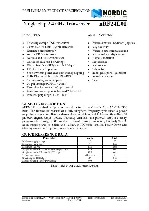
nRF24L01Single chip 2.4 GHz TransceiverFEATURES APPLICATIONS•True single chip GFSK transceiver •Wireless mouse, keyboard, joystick •Complete OSI Link Layer in hardware •Keyless entry•Enhanced ShockBurst™ •Wireless data communication•Auto ACK & retransmit •Alarm and security systems•Address and CRC computation •Home automation•On the air data rate 1 or 2Mbps •Surveillance•Digital interface (SPI) speed 0-8 Mbps •Automotive•125 RF channel operation •Telemetry•Short switching time enable frequency hopping •Intelligent sports equipment•Fully RF compatible with nRF24XX •Industrial sensors•5V tolerant signal input pads •Toys•20-pin package (QFN20 4x4mm)•Uses ultra low cost +/- 60 ppm crystal•Uses low cost chip inductors and 2-layer PCB•Power supply range: 1.9 to 3.6 VGENERAL DESCRIPTIONnRF24L01 is a single chip radio transceiver for the world wide 2.4 - 2.5 GHz ISMband. The transceiver consists of a fully integrated frequency synthesizer, a poweramplifier, a crystal oscillator, a demodulator, modulator and Enhanced ShockBurst™protocol engine. Output power, frequency channels, and protocol setup are easily programmable through a SPI interface. Current consumption is very low, only 9.0mAat an output power of -6dBm and 12.3mA in RX mode. Built-in Power Down andStandby modes makes power saving easily realizable.QUICK REFERENCE DATAUnit Parameter ValueMinimum supply voltage 1.9 VMaximum output power 0 dBmMaximum data rate 2000 kbpsSupply current in TX mode @ 0dBm output power 11.3 mASupply current in RX mode @ 2000 kbps 12.3 mATemperature range -40 to +85 °CSensitivity @ 1000 kbps -85 dBmSupply current in Power Down mode 900 nATable 1 nRF24L01 quick reference dataType NumberDescriptionVersionnRF24L01 20 pin QFN 4x4, RoHS & SS-00259 compliantD nRF24L01 IC Bare DiceD nRF24L01-EVKITEvaluation kit (2 test PCB, 2 configuration PCB, SW)1.0Table 2 nRF24L01 ordering informationBLOCK DIAGRAMDDD=0VD=0V=0VFigure 1 nRF24L01 with external components.PIN FUNCTIONSPin NamePin function Description1 CEDigital InputChip Enable Activates RX or TX mode2 CSN Digital InputSPI Chip Select 3SCK Digital InputSPI Clock4 MOSIDigital InputSPI Slave Data Input5 MISO Digital Output SPI Slave Data Output, with tri-state option6 IRQ Digital Output Maskable interrupt pin7 VDDPowerPower Supply (+3V DC) 8 VSS Power Ground (0V) 9 XC2 Analog Output Crystal Pin 2 10 XC1 Analog Input Crystal Pin 111 VDD_PA Power Output Power Supply (+1.8V) to Power Amplifier 12 ANT1 RF Antenna interface 1 13 ANT2 RFAntenna interface 2 14 VSS Power Ground (0V)15 VDD PowerPower Supply (+3V DC) 16 IREF Analog Input Reference current 17 VSS Power Ground (0V)18 VDD PowerPower Supply (+3V DC)19 DVDD Power Output Positive Digital Supply output for de-coupling purposes 20 VSSPowerGround (0V)Table 3 nRF24L01 pin functionPIN ASSIGNMENTVDDVSSANT2VSSCEVDD_PAANT1CSNMISO MOSI VDDIREFVSSIRQDVDDVSSXC2XC1VDDSCKFigure 2 nRF24L01 pin assignment (top view) for a QFN20 4x4 package.ELECTRICAL SPECIFICATIONSConditions: VDD = +3V, VSS = 0V, T A = - 40ºC to + 85ºCymbol Parameter (condition)NotesMin.Typ.Max. UnitsOperating conditionsVDD Supply voltage1.9 3.0 3.6 V TEMP Operating Temperature-40+27+85ºCDigital input pinV IH HIGH level input voltage 10.7VDD 5.25 VV IL LOW level input voltageVSS 0.3VDD VDigital output pinV OH HIGH level output voltage (I OH =-0.25m A ) VDD- 0.3 VDD VV OL LOW level output voltage (I OL =0.25m A) VSS 0.3 VGeneral RF conditionsf OP Operating frequency22400 2525 MHzf XTAL Crystal frequency16 MHz ∆f 1MFrequency deviation @ 1000kbps ±160 kHz ∆f 2MFrequency deviation @ 2000kbps ±320 kHz R GFSK Data rate ShockBurst™>0 2000 kbps F CHANNEL Channel spacing @ 1000kbps1 MHz F CHANNEL Channel spacing @ 2000kbps2 MHzTransmitter operationP RF Maximum Output Power30 +4 dBmP RFC RF Power Control Range 16 18 20 dB P RFCR RF Power A ccuracy ±4 dB P BW 20dB Bandwidth for Modulated Carrier(2000kbps)1800 2000 kHzP RF1 1st Adjacent Channel Transmit Power 2MHz -20 dBm P RF2 2nd Adjacent Channel Transmit Power 4MHz -50 dBm I VDD Supply current @ 0dBm output power 4 11.3 m AI VDD Supply current @ -18dBm output power 7.0m A I VDD Average Supply current @ -6dBm outputpower, Enhanced ShockBurst™50.05 m AI VDD Supply current in Standby-I mode 632 µA I VDD Supply current in power down900 nA1All digital inputs handle up to 5.25V signal inputs. Keep in mind that the VDD of the nRF24L01 must match theV IH of the driving device for output pins.2 Usable band is determined by local regulations 3Antenna load impedance = 15Ω+j88Ω 4Antenna load impedance = 15Ω+j88Ω. Effective data rate 1000kbps or 2000 kbps 5Antenna load impedance = 15Ω+j88Ω. Effective data rate 10kbps and full packets6Given for a 12pF crystal. Current when using external clock is dependent on signal swing.Receiver operationI VDD Supply current one channel 2000kbps 12.3 mAI VDD Supply current one channel 1000kbps 11.8 mARX SENS Sensitivity at 0.1%BER (@2000kbps) -82 dBm RX SENS Sensitivity at 0.1%BER (@1000kbps) -85 dBm C/I CO C/I Co-channel (@2000kbps) 778/119dB C/I1ST1st Adjacent Channel Selectivity C/I 2MHz 1/4 dB C/I2ND2nd Adjacent Channel Selectivity C/I 4MHz -21/-20 dB C/I3RD3rd Adjacent Channel Selectivity C/I 6MHz -27/-27 dB C/I CO C/I Co-channel (@1000kbps) 10911/1212dB C/I1ST1st Adjacent Channel Selectivity C/I 1MHz 8/8 dB C/I2ND2nd Adjacent Channel Selectivity C/I 2MHz -22/-21 dB C/I3RD3rd Adjacent Channel Selectivity C/I 3MHz -30/-30 dBTable 4 nRF24L01 RF specifications7Data rate is 2000kbps for the following C/I measurements8 According to ETSI EN 300 440-1 V1.3.1 (2001-09) page 279 nRF24L01 equal modulation on interfering signal10Data rate is 1000kbps for the following C/I measurements11 According to ETSI EN 300 440-1 V1.3.1 (2001-09) page 2712 nRF24L01 equal modulation on interfering signalPACKAGE OUTLINEnRF24L01 uses the QFN20 4x4 package, with matt tin plating.Package Type A A1 A3 K D/E e D2/E2 L L1 bSaw QFN20 (4x4 mm) MinTyp.Max0.800.850.950.000.020.050.20REF.0.20min4.0 BSC130.5 BSC2.502.602.700.350.400.450.15max0.180.250.30Figure 3 nRF24L01 Package Outline.13 BSC: Basic Spacing between Centers, ref. JEDEC standard 95, page 4.17-11/APackage marking:Abbreviations: B – Build Code, i.e. unique code for production sites, package type and test platform X – "X" grade, i.e. Engineering Samples (optional) YY – 2 digit Year number WW – 2 digit Week numberLL – 2 letter wafer lot number codeAbsolute Maximum RatingsSupply voltagesVDD............................- 0.3V to + 3.6V VSS..................................................0V Input voltageV I ..................................- 0.3V to 5.25V Output voltageV O .....................................VSS to VDDTotal Power DissipationP D (T A =85°C).............................60mWTemperaturesOperating Temperature…. - 40°C to + 85°C Storage Temperature….… - 40°C to + 125°CNote: Stress exceeding one or more of the limiting values may cause permanent damage to the device.ATTENTION!Electrostatic Sensitive Device Observe Precaution for handling.Glossary of Termsn R FB X2 4 L0 1 Y Y W W L LTerm DescriptionA CKAcknowledgementARTAutoRe-TransmitCE ChipEnableCLK ClockCRC Cyclic Redundancy CheckCSN ChipSelectNOTESB EnhancedShockBurst™ GFSK Gaussian Frequency Shift KeyingIRQ InterruptRequestISM Industrial-Scientific-Medical LNA LowNoiseAmplifierLSB Least Significant BitLSByte Least Significant ByteMbps Megabit per secondMCU Micro Controller UnitMISO Master In Slave OutMOSI Master Out Slave InMSB Most Significant BitMSByte Most Significant BytePCB Printed Circuit BoardPER Packet Error RatePID Packet Identity BitsPLD PayloadPRX PrimaryRXPTX PrimaryTXPWR_DWN PowerDownPWR_UP PowerUpRoHS Restriction of use of Certain Hazardous Substances RX ReceiveRX_DR Receive Data ReadySPI SerialPeripheralInterfaceTX TransmitTX_DS Transmit Data SentTable 5 GlossaryFUNCTIONAL DESCRIPTIONModes of operationThe nRF24L01 can be set in the following main modes depending on the level of the following primary I/Os and configuration registers:Mode PWR_UPregisterPRIM_RXregisterCE FIFOstateRX mode 1 1 1 -TX mode 1 0 1 Data in TX FIFOTX mode 1 0 1Î0 Stays in TX mode until packettransmission is finishedStandby-II 1 0 1 TX FIFO emptyStandby-I 1 - 0 No ongoing packet transmissionPower Down 0 - - -Table 6 nRF24L01 main modesAn overview of the nRF24L01 I/O pins in different modes is given in Table 7.Pin functions in the different modes of nRF24L01Pin Name Direction TX Mode RX Mode Standby Modes Power Down CE Input High Pulse >10µs High Low - CSN Input SPI Chip Select, active lowSCK Input SPIClock MOSI Input SPI Serial InputMISO Tri-stateOutputSPI Serial OutputIRQ Output Interrupt, active lowTable 7 Pin functions of the nRF24L01Standby ModesStandby-I mode is used to minimize average current consumption while maintaining short start up times. In this mode, part of the crystal oscillator is active. In Standby-II mode some extra clock buffers are active compared to Standby-I mode. Standby-II occurs when CE is held high on a PTX device with empty TX FIFO. The configuration word content is maintained during Standby modes. SPI interface may be activated. For start up time see Table 13.Power Down ModeIn power down nRF24L01 is disabled with minimal current consumption. When entering this mode the device is not active, but all registers values available from theSPI interface are maintained during power down and the SPI interface may be activated (CSN=0). For start up time see Table 13. The power down is controlled bythe PWR_UP bit in the CONFIG register.PRELIMINARY PRODUCT SPECIFICATIONnRF24L01 Single Chip 2.4 GHz Radio TransceiverPacket Handling MethodsnRF24L01 has the following Packet Handling Methods: • ShockBurst™ (compatible with nRF2401, nRF24E1, nRF2402 and nRF24E2 with 1Mbps data rate, see page 26) • Enhanced ShockBurst™ShockBurst™ShockBurst™ makes it possible to use the high data rate offered by nRF24L01 without the need of a costly, high-speed microcontroller (MCU) for data processing/clock recovery. By placing all high speed signal processing related to RF protocol on-chip, nRF24L01 offers the application microcontroller a simple SPI compatible interface, the data rate is decided by the interface-speed the micro controller itself sets up. By allowing the digital part of the application to run at low speed, while maximizing the data rate on the RF link, ShockBurst™ reduces the average current consumption in applications. In ShockBurst™ RX, IRQ notifies the MCU when a valid address and payload is received respectively. The MCU can then clock out the received payload from an nRF24L01 RX FIFO. In ShockBurst™ TX, nRF24L01 automatically generates preamble and CRC, see Table 12. IRQ notifies the MCU that the transmission is completed. All together, this means reduced memory demand in the MCU resulting in a low cost MCU, as well as reduced software development time. nRF24L01 has a three level deep RX FIFO (shared between 6 pipes) and a three level deep TX FIFO. The MCU can access the FIFOs at any time, in power down mode, in standby modes, and during RF packet transmission. This allows the slowest possible SPI interface compared to the average data-rate, and may enable usage of an MCU without hardware SPI.Enhanced ShockBurst™Enhanced ShockBurst™ is a packet handling method with functionality that makes bidirectional link protocol implementation easier and more efficient. In a typical bidirectional link, one will let the terminating part acknowledge received packets from the originating part in order to make it possible to detect data loss. Data loss can then be recovered by retransmission. The idea with Enhanced ShockBurst™ is to let nRF24L01 handle both acknowledgement of received packets and retransmissions of lost packets, without involvement from the microcontroller.Nordic Semiconductor ASA Revision: 1.2- Vestre Rosten 81, N-7075 Tiller, Norway-Phone +4772898900-Page 11 of 39Fax +4772898989 March 2006PRELIMINARY PRODUCT SPECIFICATIONnRF24L01 Single Chip 2.4 GHz Radio TransceiverTX3 TX2ipe 4P DataTX4 TX5Data PData PDa taTX1ipe 1PipeFigure 4: nRF24L01 in a star network configuration An nRF24L01 configured as primary RX (PRX) will be able to receive data trough 6 different data pipes, see Figure 4. A data pipe will have a unique address but share the same frequency channel. This means that up to 6 different nRF24L01 configured as primary TX (PTX) can communicate with one nRF24L01 configured as PRX, and the nRF24L01 configured as PRX will be able to distinguish between them. Data pipe 0 has a unique 40 bit configurable address. Each of data pipe 1-5 has an 8 bit unique address and shares the 32 most significant address bits. All data pipes can perform full Enhanced ShockBurst™ functionality. nRF24L01 will use the data pipe address when acknowledging a received packet. This means that nRF24L01 will transmit ACK with the same address as it receives payload at. In the PTX device data pipe 0 is used to received the acknowledgement, and therefore the receive address for data pipe 0 has to be equal to the transmit address to be able to receive the acknowledgement. See Figure 5 for addressing example.t Da a pe Pi 25Frequency Channel Nipe 3TX6Da 0 ipe ta PRXNordic Semiconductor ASA Revision: 1.2- Vestre Rosten 81, N-7075 Tiller, Norway-Phone +4772898900-Page 12 of 39Fax +4772898989 March 2006PRELIMINARY PRODUCT SPECIFICATIONnRF24L01 Single Chip 2.4 GHz Radio TransceiverFigure 5: Example on how the acknowledgement addressing is done An nRF24L01 configured as PTX with Enhanced ShockBurst™ enabled, will use the ShockBurst™ feature to send a packet whenever the microcontroller wants to. After the packet has been transmitted, nRF24L01 will switch on its receiver and expect an acknowledgement to arrive from the terminating part. If this acknowledgement fails to arrive, nRF24L01 will retransmit the same packet until it receives an acknowledgement or the number of retries exceeds the number of allowed retries given in the SETUP_RETR_ARC register. If the number of retries exceeds the number of allowed retries, this will be showed by the STATUS register bit MAX_RT which gives an interrupt. Whenever an acknowledgement is received by an nRF24L01 it will consider the last transmitted packet as delivered. It will then be cleared from the TX FIFO, and the TX_DS IRQ source will be set high. With Enhanced ShockBurst™ nRF24L01 offers the following benefits: • Highly reduced current consumption due to short time on air and sharp timing when operating with acknowledgement traffic • Lower system cost. Since the nRF24L01 handles all the high-speed link layer operations, like re-transmission of lost packet and generating acknowledgement to received packets, it is no need for hardware SPI on the system microcontroller to interface the nRF24L01. The interface can be done by using general purpose IO pins on a low cost microcontroller where the SPI is emulated in firmware. With the nRF24L01 this will be sufficient speed even when running a bi-directional link. • Greatly reduced risk of “on-air” collisions due to short time on air • Easier firmware development since the link layer is integrated on chipNordic Semiconductor ASA Revision: 1.2 - Vestre Rosten 81, N-7075 Tiller, Norway Phone +4772898900 -Page 13 of 39Fax +4772898989 March 2006PRELIMINARY PRODUCT SPECIFICATIONnRF24L01 Single Chip 2.4 GHz Radio TransceiverEnhanced ShockBurst™ Transmitting Payload:1. The configuration bit PRIM_RX has to be low. 2. When the application MCU has data to send, the address for receiving node (TX_ADDR) and payload data (TX_PLD) has to be clocked into nRF24L01 via the SPI interface. The width of TX-payload is counted from number of bytes written into the TX FIFO from the MCU. TX_PLD must be written continuously while holding CSN low. TX_ADDR does not have to be rewritten if it is unchanged from last transmit. If the PTX device shall receive acknowledge, data pipe 0 has to be configured to receive the acknowledgement. The receive address for data pipe 0 (RX_ADDR_P0) has to be equal to the transmit address (TX_ADDR) in the PTX device. For the example in Figure 5 the following address settings have to be performed for the TX5 device and the RX device: TX5 device: TX_ADDR = 0xB3B4B5B605 TX5 device: RX_ADDR_P0 = 0xB3B4B5B605 RX device: RX_ADDR_P5 = 0xB3B4B5B605 3. A high pulse on CE starts the transmission. The minimum pulse width on CE is 10 µs. 4. nRF24L01 ShockBurst™: • Radio is powered up • 16 MHz internal clock is started. • RF packet is completed (see the packet description) • Data is transmitted at high speed (1 Mbps or 2 Mbps configured by MCU). 5. If auto acknowledgement is activated (ENAA_P0=1) the radio goes into RX mode immediately. If a valid packet has been received in the valid acknowledgement time window, the transmission is considered a success. The TX_DS bit in the status register is set high and the payload is removed from TX FIFO. If a valid acknowledgement is not received in the specified time window, the payload is resent (if auto retransmit is enabled). If the auto retransmit counter (ARC_CNT) exceeds the programmed maximum limit (ARC), the MAX_RT bit in the status register is set high. The payload in TX FIFO is NOT removed. The IRQ pin will be active when MAX_RT or TX_DS is high. To turn off the IRQ pin, the interrupt source must be reset by writing to the status register (see Interrupt chapter). If no acknowledgement is received for a packet after the maximum number of retries, no further packets can be sent before the MAX_RX interrupt is cleared. The packet loss counter (PLOS_CNT) is incremented at each MAX_RT interrupt. I.e. ARC_CNT counts the number of retries that was required to get a single packet through. PLOS_CNT counts the number of packets that did not get through after maximum number of retries. 6. The device goes into Standby-I mode if CE is low. Otherwise next payload in TX FIFO will be sent. If TX FIFO is empty and CE is still high, the device will enter Standby-II mode. 7. If the device is in Standby-II mode, it will go to Standby-I mode immediately if CE is set low.Enhanced ShockBurstTM Receive Payload:1. RX is selected by setting the PRIM_RX bit in the configuration register to high. All data pipes that shall receive data must be enabled (EN_RXADDR register),Nordic Semiconductor ASA Revision: 1.2 - Vestre Rosten 81, N-7075 Tiller, Norway Phone +4772898900 Fax +4772898989 March 2006Page 14 of 39PRELIMINARY PRODUCT SPECIFICATIONnRF24L01 Single Chip 2.4 GHz Radio Transceiver2. 3. 4.5. 6. 7. 8.auto acknowledgement for all pipes running Enhanced ShockBurst™ has to be enabled (EN_AA register), and the correct payload widths must be set (RX_PW_Px registers). Addresses have to be set up as described in item 2 in the Enhanced ShockBurst™ transmit payload chapter above. Active RX mode is started by setting CE high. After 130µs nRF24L01 is monitoring the air for incoming communication. When a valid packet has been received (matching address and correct CRC), the payload is stored in the RX-FIFO, and the RX_DR bit in status register is set high. The IRQ pin will be active when RX_DR is high. RX_P_NO in status register will indicate what data pipe the payload has been received in. If auto acknowledgement is enabled, an acknowledgement is sent back. MCU sets the CE pin low to enter Standby-I mode (low current mode). MCU can clock out the payload data at a suitable rate via the SPI interface. The device is now ready for entering TX or RX mode or power down mode.Two way communication with payload in both directionsIf payload shall be sent in both directions, the PRIM_RX register must be toggled by redefining the device from PRX to PTX or vice versa. The controlling processors must handle the synchronicity between a PTX and a PRX. Data buffering in both RX FIFO and TX FIFO simultaneously is possible, but restricted to data pipes 1 to 5. The third level in TX FIFO shall only be written in RX, TX or Standby-II mode if data is stored in RX FIFOAuto Acknowledgement (RX)The auto acknowledgement function reduces the load of the external microcontroller, and may remove the need for dedicated SPI hardware in a mouse/keyboard or comparable systems, and hence reduce cost and average current consumption. Auto acknowledgement can be configured individually for each data pipe via the SPI interface. If auto acknowledgement is enabled and a valid packet (correct data pipe address and CRC) is received, the device will enter TX mode and send an acknowledgement packet. After the device has sent the acknowledgement packet, normal operation resumes, and the mode is determined by the PRIM_RX register and CE pin.Auto Re-Transmission (ART) (TX)An auto retransmission function is available. It will be used at the TX side in an auto acknowledgement system. In the SETUP_RETR register it will be possible to state how many times the data in the data register will be resent if data is not acknowledged. After each sending, the device will enter RX mode and wait a specified time period for acknowledgement. When the acknowledgement packet is received, the device will return to normal transmit function. If there is no more unsent data in the TX FIFO and the CE pin is low, the device will go into Standby-I mode. If the acknowledgement is not received, the device will go back to TX mode and resend the data. This will continue until acknowledgment is received, or a time out occursNordic Semiconductor ASA Revision: 1.2 - Vestre Rosten 81, N-7075 Tiller, Norway Phone +4772898900 Fax +4772898989 March 2006Page 15 of 39PRELIMINARY PRODUCT SPECIFICATIONnRF24L01 Single Chip 2.4 GHz Radio Transceiver(i.e. the maximum number of sending is reached). The only way to reset this is to set the PWR_UP bit low or let the auto retransmission finish. A packet loss counter will be incremented each time a packet does not succeed to reach the destination before time out. (Time out is indicated by the MAX_RT interrupt.) The packet loss counter is reset when writing to the RF channel register.Packet Identity (PID) and CRC used by Enhanced ShockBurstTMEach packet contains a two bit wide PID field to detect if the received packet is new or resent. The PID will prevent that the PRX device presents the same payload more than once to the microcontroller. This PID field is incremented at the TX side for each new packet received via the SPI interface. The PID and CRC field is used by the PRX device to determine whether a packet is resent or new. When several data is lost on the link, the PID fields may in some cases become equal to last received PID. If a packet has the same PID as the previous packet, nRF24L01 will compare the CRC sums from both packets. If they also are equal, the last received packet is considered as a copy of the previous and is discarded. 1: PRX device: The PRX device compares the received PID with the last PID. If the PID fields are different, the packet is considered to be new. If the PID is equal to last received PID, the received packet might be the same as last time. The receiver must check if the CRC is equal to the previous CRC. If the CRC is equal to the previous one, the packet is probably the same, and will be discarded. 2: PTX device: The transmitter increments the PID field each time it sends a new packet.TX side functionalityStartRX side functionalityStartNew packet from MCU?YesPID equal last PID?YesCRC equal last CRC?increment PID No No New packet is valid for MCUYes NoDiscard packet as a copyEndEndFigure 6 PID generation/detectionNordic Semiconductor ASA Revision: 1.2 - Vestre Rosten 81, N-7075 Tiller, Norway Phone +4772898900 Fax +4772898989 March 2006Page 16 of 39PRELIMINARY PRODUCT SPECIFICATIONnRF24L01 Single Chip 2.4 GHz Radio TransceiverThe length of the CRC is configurable through the SPI interface. It is important to notice that the CRC is calculated over the whole packet including address, PID and payload. No packet is accepted as correct if the CRC fails. This is an extra requirement for packet acceptance that is not illustrated in the figure above.Stationary Disturbance Detection – CDCarrier Detect (CD) is set high when an in-band RF signal is detected in RX mode, otherwise CD is low. The internal CD signal is filtered before presented to CD register. The internal CD signal must be high for at least 128µs. In Enhanced ShockBurst™ it is recommended to use the Carrier Detect functionality only when the PTX device does not succeed to get packets through, as indicated by the MAX_RT interrupt for single packets and by the packet loss counter (PLOS_CNT) if several packets are lost. If the PLOS_CNT in the PTX device indicates to high rate of packet losses, the device can be configured to a PRX device for a short time (Tstbt2a + CD-filter delay = 130µs+128µs = 258µs) to check CD. If CD was high (jam situation), the frequency channel should be changed. If CD was low (out of range), it may continue on the same frequency channel, but perform other adjustments. (A dummy write to the RF_CH will clear the PLOS_CNT.)Data PipesnRF24L01 configured as PRX can receive data addressed to 6 different data pipes in one physical frequency channel. Each data pipe has its own unique address and can be configured to have individual behavior. The data pipes are enabled with the bits in the EN_RXADDR register. By default only data pipe 0 and 1 are enabled. The address for each data pipe is configured in the RX_ADDR_Px registers. Always ensure that none of the data pipes have the exact same address. Data pipe 0 has a unique 40 bit configurable address. Data pipes 1-5 share the 32 most significant address bits and have only the LSByte unique for each data pipe. Figure 7 shows an example of how data pipes 0-5 are addressed. All pipes can have up to 40 bit address, but for pipe 1-5 only the LSByte is different, and the LSByte must be unique for all pipes.Nordic Semiconductor ASA Revision: 1.2- Vestre Rosten 81, N-7075 Tiller, Norway-Phone +4772898900-Page 17 of 39Fax +4772898989 March 2006PRELIMINARY PRODUCT SPECIFICATIONnRF24L01 Single Chip 2.4 GHz Radio TransceiverByte 4 Data pipe 0 (RX_ADDR_P0) Data pipe 1 (RX_ADDR_P1) Data pipe 2 (RX_ADDR_P2) Data pipe 3 (RX_ADDR_P3) Data pipe 4 (RX_ADDR_P4) Data pipe 5 (RX_ADDR_P5) 0xE7 0xC2 0xC2 0xC2 0xC2 0xC2 Byte 3 0xD3 0xC2 0xC2 0xC2 0xC2 0xC2 Byte 2 0xF0 0xC2 0xC2 0xC2 0xC2 0xC2 Byte 1 0x35 0xC2 0xC2 0xC2 0xC2 0xC2 Byte 0 0x77 0xC2 0xC3 0xC4 0xC5 0xC6Figure 7: Addressing data pipes 0-5 When a packet has been received at one of the data pipes and the data pipe is setup to generate acknowledgement, nRF24L01 will generate an acknowledgement with an address that equals the data pipe address where the packet was received. Some configuration settings are common to all data pipes and some are individual. The following settings are common to all data pipes: • CRC enabled/disabled (CRC always enabled when ESB is enabled) • CRC encoding scheme • RX address width • Frequency channel • RF data rate • LNA gain • RF output powerNordic Semiconductor ASA Revision: 1.2- Vestre Rosten 81, N-7075 Tiller, Norway-Phone +4772898900-Page 18 of 39Fax +4772898989 March 2006。

配电自动化馈线终端(FTU)技术规范目录1 规范性引用文件 (1)2 技术要求 (1)3 标准技术参数 (10)4 环境条件表 (12)5 试验 (13)附录A馈线终端无线通信安装位置、航插尺寸定义(参考性附录) (14)附录B 馈线终端接口定义(规范性附录) (28)配电自动化馈线终端(FTU)技术规范1 规范性引用文件下列文件对于本文件的应用是必不可少的。
凡是注日期的引用文件,仅注日期的版本适用于本文件。
凡是不注日期的引用文件,其最新版本适用于本文件。
GB/T 17626.1 电磁兼容试验和测量技术抗扰度试验总论GB/T 17626.2 静电放电抗扰度试验GB/T 17626.3 射频电磁场辐射抗扰度试验GB/T 17626.4 浪涌(冲击)抗扰度试验GB/T 17626.5 电快速瞬变脉冲群抗扰度试验GB/T 17626.8 工频磁场的抗扰度试验GB/T 17626.10 阻尼振荡磁场的抗扰度试验GB/T 17626.11 电压暂降、短时中断和电压变化抗扰度试验GB/T 15153.1 远动设备及系统第2部分:工作条件第1篇:电源和电磁兼容兼容性GB/T 11022 高压开关设备和控制设备标准的共用技术要求GB/T 14285 继电保护和安全自动装置技术规程GB/T 4208 外壳防护等级(IP)GB/T 13729 远动终端设备GB/T 5096 电子设备用机电件基本试验规程及测量方法GB/T 19520 电子设备机械结构GB 7251.5 低压成套开关设备和控制设备第五部分:对户外公共场所的成套设备—动力配电网用电缆分线箱(CDCs)的特殊要求DL/T 637-1997 阀控式密封铅酸蓄电池订货技术条件DL/T 721 配电网自动化系统远方终端DL/T 634.5101 远动设备及系统第5-101部分:传输规约基本远动任务配套标准DL/T 634.5104 远动设备及系统第5-104部分:传输规约采用标准传输协议子集的IEC60870-5-101网络访问DL/T 814 配电自动化系统功能规范Q/GDW 382 配电自动化技术导则Q/GDW 513 配电自动化主站系统功能规范Q/GDW 514 配电自动化终端/子站功能规范Q/GDW 625 配电自动化建设与改造标准化设计技术规定2技术要求2.1概述馈线终端的结构形式可分为箱式馈线终端和罩式馈线终端。
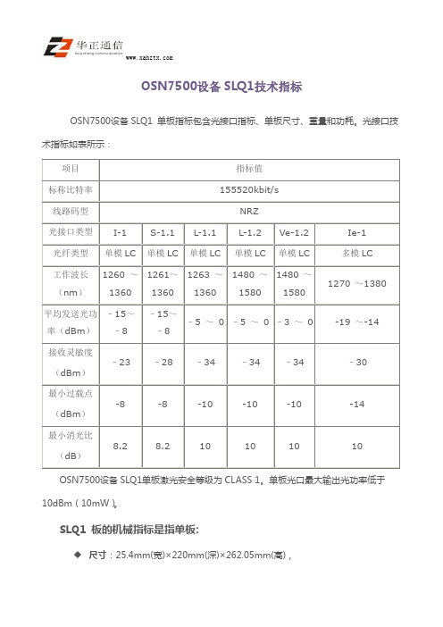
OSN7500设备SLQ1技术指标
OSN7500设备SLQ1 单板指标包含光接口指标、单板尺寸、重量和功耗。
光接口技术指标如表所示:
项目指标值
标称比特率155520kbit/s
线路码型NRZ
光接口类型I-1 S-1.1 L-1.1 L-1.2 Ve-1.2 Ie-1
光纤类型单模LC 单模LC 单模LC 单模LC 单模LC 多模LC
工作波长(nm)1260 ~
1360
1261~
1360
1263 ~
1360
1480 ~
1580
1480 ~
1580
1270 ~1380
平均发送光功率(dBm)–15~
–8
–15~
–8
–5 ~0 –5 ~0 –3 ~0 -19 ~-14
接收灵敏度
(dBm)
–23 –28 –34 –34 –34 –30
最小过载点
(dBm)
-8 -8 -10 -10 -10 -14
最小消光比
(dB)
8.2 8.2 10 10 10 10
OSN7500设备SLQ1单板激光安全等级为CLASS 1。
单板光口最大输出光功率低于10dBm(10mW)。
SLQ1 板的机械指标是指单板:
尺寸:25.4mm(宽)×220mm(深)×262.05mm(高),
◆重量:1.0KG
◆功耗:SLQ1 板在常温(25℃)条件下的最大功耗为15W。
◆单板面板上的指示灯有:单板硬件状态灯(STAT)红绿双色指示灯、业务激活状
态灯(ACT)绿色指示灯、单板软件状态灯(PROG)红绿双色指示灯及业务告警指示灯(SRV)红、绿、黄三色指示灯。

第一部分光纤收发器FT-100A 快速以太网光纤收发器系列FT-101A快速以太网光纤收发器系列FT-200A千兆以太网光纤收发器系列FT-200千兆以太网光纤收发器系列FT-120A双电口光纤收发器系列FT-150A四电口光纤收发器系列FTC-8光纤收发器机箱FTC-14光纤收发器机架FTC-16光纤收发器机架FT-100A 快速以太网光纤收发器系列概述:OpOne FT-100A为10/100Mbps自适应快速以太网光纤收发器(亦称光电介质转换器),可将10Base-T和100Base-TX双绞线电信号同100Base-FX光信号进行相互转换。
使网络的传输距离从铜线100m的极限扩展到120Km(单模全双工方式)。
支持两种不同的网络连接媒体类型:10/100Base-TX和100Base-FX,通过使用交换技术和存储转发技术来实现两种网络连接媒体之间的数据传输。
支持双纤多模、双纤单模和单纤单模多种光纤传输。
特点:自动适应10Mbps和100Mbps环境,便于网络的升级内置高效交换核心,实现流量控制,减少广播包支持全双工和半双工传输模式,能自动协商支持双绞线口自动交叉,方便系统调试安装支持最长1552byte超长数据包传输支持VLAN标签超长数据包传输支持QoS,保证VOIP数据包传输支持STP生成树,构成冗余网络低功耗,低发热,能长时间稳定工作;支持双纤多模、双纤单模和单纤单模多种光纤口选择,扩展了用户的需求。
产品图片:FT-100A(双纤单/多模外置电源) FT-100APS(单纤单模内置电源) FT-100AC(双纤单纤单模块卡)参数规格接入方式10/100Mbps标准IEEE802.3 10Base-T Ethernet,IEEE802.3u,100Base-TX/FX Fast Ethernet, IEEE802.3x Flow control,IEEE802.1q VLAN,IEEE802.1p QoS,IEEE802.1d Spanning Tree波长850nm/1310nm/1550nm传输距离双纤多模:2Km,双纤单模:25/40/60/80/100/120Km,单纤单模:25/40/60/80/100Km五类双绞线:100m端口1个RJ45口:连接STP/UTP五类双绞线1个光纤口:多模—SC或ST(光纤尺寸50、62.5/125μm)订购信息:FT-101A快速以太网光纤收发器系列概述:OpOne FT-101A为10/100M自适应快速以太网光纤收发器(亦称光电介质转换器),可将10Base-T和100Base-TX双绞线电信号同100Base-FX光信号进行相互转换。

韩国三荣电子通信公司SAMYUNG ENC注意:请用户使用前务必详阅此说明书。
目 录1 概述-----------------------------2 8 打印机使用---------------------37 1.1 特点-----------------------------2 8.1 DPU-414打印机-----------------37 1.2 基本配置-------------------------2 9 电路---------------------------39 2 特性-----------------------------3 9.1 概述---------------------------39 2.1 技术指标-------------------------3 9.2 电源电路-----------------------39 2.2 中高频发射机---------------------3 9.3 发射电路-----------------------39 2.3 中高频接收机---------------------4 9.4 MF/HF接收电路-----------------39 2.4 DSC控制-------------------------5 9.5 母板(T-550)------------------40 2.5 自动报警-------------------------5 9.6 发射滤波器(T-451)------------40 2.6 中高频控制-----------------------6 9.7 合成器单元(T-553)------------402.7 2.8 数字选择性呼叫(DSC)------------6打印机(DPU-414)----------------69.89.9电源控制(T-555)--------------40功率放大器(T514)-------------413 电源-----------------------------8 9.10 控制(T-557)------------------41 3.1 电源输入-------------------------8 9.11 面板(T-568)------------------41 3.2 交流供电-------------------------8 9.12 值守接收机(T-552)------------41 3.3 直流供电-------------------------8 9.13 接收后板功能示意图-------------42 3.4 电池充电-------------------------84 面板-----------------------------94.1 按钮、旋钮、指示灯说明-----------94.2 液晶显示器----------------------104.3 菜单结构------------------------115 单边带无线电话模式--------------135.1 单边带无线电话模式--------------135.2 单边带菜单显示------------------136 数字选择性呼叫模式--------------176.1 数字选择性呼叫模式选择----------176.2 数字选择性呼叫菜单显示----------177 遇险信号发射--------------------367.1 2182KHz遇险报警信号的发射------367.2 2182KHz遇险报警信号的测试------361、 概述此设备用于自动数字系统通信,包括遇险安全和一般通信,由MF/HF收发机、自动报警系统、数字选择性呼叫组成。

MK32工业级手持地面站用户手册V1.12023.10感谢您购买思翼科技的产品。
MK32工业级手持地面站是思翼科技链路产品家族的最新成员,搭载7英寸高清高亮大屏、可扩展至30KM的双路全高清数字图传、4G运存和64G存储的顶级安卓配置,还可选购一机双控、遥控接力等特性,丰富的接口和强大的可扩展性可广泛应用于无人机、无人车船以及智能机器人等领域。
考虑到飞行安全,也为了带给您良好的产品使用体验,请您在装机、飞行前仔细查阅用户手册。
本手册可以帮助您解决大部分的使用疑问,您也可以通过访问思翼科技官方网站()与本产品相关的页面,致电思翼科技官方售后服务中心(400-8382918)或者发送邮件到****************直接向思翼科技工程师咨询产品相关知识以及反馈产品问题。
思翼科技官方QQ群说明书版本更新记录阅读提示 (8)标识、图标 (8)安全 (8)电池 (10)设备闲置、携带、回收 (10)1 产品简介 (12)1.1 产品特性 (12)1.2 部件说明 (14)1.2.1 产品概览 (14)1.2.2 按键、开关类型及通道定义 (16)1.2.3 接口与数据流 (17)1.3 技术参数 (20)1.4 物品清单 (25)1.5 状态指示灯定义 (27)1.5.1 遥控器指示灯定义 (27)1.5.2 天空端指示灯定义 (28)2 使用前 (29)2.1 地面端 (29)2.1.1 开机与关机 (29)2.1.2 充电 (29)2.1.3 充电指示灯定义 (30)2.1.4 切换系统语言 (30)2.2 提升通讯距离与视频流畅性重要说明 (34)2.2.1 使用注意事项 (34)2.2.2 不同飞行距离需求下天线选用以及无线飞行模式设置方法 (34)2.2.3 地面端标准全向天线的安装摆放方式 (35)2.2.4 地面端平板增程天线的安装摆放方式 (36)2.2.5 天空端标准全向天线的安装摆放方式 (37)2.2.6 通讯距离不理想、需要原厂技术支持前所需必要信息 (41)3 “思翼遥控”应用 (43)3.1 通道设置 (44)3.1.1 舵机行程量 (44)3.1.2 中立点调节 (44)3.1.3 舵机反向 (45)3.1.4 通道映射 (45)3.2 数传设置 (47)3.2.1 连接 (47)3.2.2 飞控 (48)3.2.3 串口波特率 (49)3.3 系统设置 (51)3.3.1 对频 (52)3.3.2 多天空端 (52)3.3.3 自适应频点 (53)3.3.4 油门杆类型 (53)3.3.5 第15通道 (54)3.3.6 无线模式 (54)3.3.7 摇杆死区 (55)3.4 链路信息 (56)3.5 失控保护 (57)3.6 按键拨轮设置 (59)3.6.1 按键设置 (59)3.6.2 拨轮设置 (59)3.7 摇杆校准 (61)3.8 拨轮校准 (64)3.9 多机互联 (67)3.9.1 遥控接力 (67)3.9.2 一机双控 (68)3.10 设备信息 (71)3.11 “思翼遥控”更新日志 (72)4 数传 (73)4.1 通过UART串口与安卓地面站通信 (73)4.1.1 极翼飞防管家 (73)4.1.2 博鹰农业 (74)4.1.3 微克智飞 (75)4.2通过USB串口与安卓地面站通信 (77)4.2.1 QGroundControl (77)4.2.2 Mission Planner (78)4.3通过蓝牙与安卓地面站通信 (80)4.3.1 QGroundControl (80)4.2.2 Mission Planner (82)4.4 通过UDP与安卓地面站通信 (84)4.4.1 QGroundControl (84)4.4.2 Mission Planner (85)4.5 通过遥控器Type-C升级接口与Windows地面站通信 (88)4.5.1 QGroundControl (88)4.5.2 Mission Planner (89)4.6 通过UDP经过遥控器WiFi热点与Windows地面站通信 (91)4.6.1 QGroundControl (91)4.6.2 Mission Planner (92)4.7 数传无法连接的解决方法 (95)4.8 数传SDK通讯协议 (97)4.8.1 协议格式说明 (97)4.8.2 通讯命令 (97)4.8.3 通讯接口 (103)4.8.4 SDK CRC16校验代码 (103)5 “SIYI FPV”应用 (107)5.1 设置菜单 (109)5.2 链路信息 (110)5.3 云台相机 (111)5.4 关于SIYI FPV (113)5.5 SIYI FPV应用更新记录 (114)6 图传 (115)6.1 思翼手持地面站配合“SIYI FPV”或思翼QGC(安卓)应用控制思翼光电吊舱/云台相机 (115)6.1.1 准备工作 (115)6.1.2 云台俯仰与平移 (117)6.1.3 变倍 (117)6.1.4 拍照与录像 (117)6.2 接入第三方网口相机或光电吊舱 (119)6.3 接入HDMI相机 (120)6.4 接入双路视频 (121)6.4.1 接入两个思翼相机或两个天空端HDMI输入模块 (121)6.4.2 接入两个第三方网口相机或光电吊舱 (121)6.4.3 接入一个思翼天空端HDMI输入模块和一个第三方网口相机或光电吊舱1216.5 设备常用参数 (123)6.6 无法显示视频图像的解决方法 (124)6.7 从遥控器输出图像至其他设备 (126)6.7.1 通过遥控器HDMI接口输出 (126)6.7.2 通过遥控器WiFi热点共享输出 (126)6.7.3 通过以太网口输出图像 (127)7 安卓系统 (132)7.1 下载应用 (132)7.2 如何导入并安装应用 (132)7.2.1 通过TF卡导入并安装 (132)7.2.2 通过U盘导入并安装 (132)7.2.3 通过Type-C文件传输功能导入并安装 (133)7.3 查看安卓固件版本 (136)8 思翼调参助手 (138)8.1 固件升级 (138)8.2 主要固件更新记录 (141)8.3 调参软件更新记录 (143)9 售后与保修 (144)9.1 返修流程 (144)9.2 保修政策 (144)9.2.1 7天包退货 (145)9.2.2 15天免费换货 (146)9.2.3 一年内免费保修 (147)阅读提示标识、图标在阅读用户手册时,请特别注意有如下标识的相关内容。
通信工程施工质量验收规范及技术标准目录第一章基站设备安装、服务技术要求 (7)1.1 设备安装标准 (7)1.1.1 机架施工标准 (7)1.1.2 电源、接地施工标准 (7)1.1.3 走线架布线施工标准 (7)1.1.4 标记方法及标准 (7)1.2 设备安装应当使用的工器具 (8)第二章天馈设备安装、服务技术要求 (9)2.1 一般规定 (9)2.2 天线支撑杆的安装 (9)2.3 天线安装 (9)2.3.1 全向天线 (9)2.3.2 定向天线 (9)2.3.3 GPS天线安装应符合下列要求 (12)2.3.4 馈线安装 (12)2.3.5 跳线安装 (13)2.3.6 避雷器的安装 (13)2.3.7 胶泥、胶带及密封夹的使用 (14)2.3.8 方位角的调整 (14)2.3.9 俯仰角的调整 (14)2.3.10 天馈线安装检查 (14)2.3.11 安装测试 (14)2.3.12 安全注意事项 (15)第三章传输设备安装、服务技术要求 (16)3.1 设备安装 (16)3.1.1 槽道、列柜安装 (16)3.1.2 机架安装 (16)3.1.3 电缆布放及成端 (17)3.2 设备检查及本机测试 (17)3.3 防雷接地线要求 (17)3.4 机架安装抗震加固措施 (18)第四章电源设备安装、服务技术要求 (19)4.1 交流配电箱安装要求 (19)4.4 走线架安装要求 (19)第五章核心机房设备安装、服务技术要求 (21)5.1 交换设备安装工艺要求 (21)5.2 电缆走线架安装工艺要求 (21)5.3 缆线布放工艺要求 (21)5.4 抗震加固要求 (22)第六章接入网设备安装、服务技术要求 (23)6.1施工前的准备 (23)6.1.1 对机房的要求 (23)6.1.2 对器材的检验 (23)6.2 设备安装 (24)6.2.1 槽道、列柜安装 (24)6.2.2 机架安装 (24)6.2.3 子架安装 (24)6.3 线缆布放及成端 (24)6.3.1 敷设电缆及光纤连接线 (24)6.3.2 编扎光纤连接线 (25)6.3.3 布放数字配线架跳线 (25)6.3.4 电缆成端和保护 (25)6.3.5 敷设电源线 (25)6.4 设备检查及本机测试 (25)第七章室内分布与WLAN覆盖集成工艺要求 (26)7.1 设备安装 (26)7.1.1 BBU、RRU安装 (26)7.1.2 直放站安装 (27)7.1.3 附件安装 (27)7.1.4 AP设备安装 (27)7.1.5 AC设备安装 (29)7.1.6 POE及汇聚交换机设备安装 (29)7.1.7 光纤分布系统设备安装 (29)7.2 GPS天线安装 (31)7.3 无源器件安装要求 (32)7.4 天线安装要求 (32)7.4.1 室外天线安装 (32)7.4.2 室内天线安装 (33)7.5.2 馈线连接头安装要求 (35)7.5.3 馈线防水要求 (35)7.5.4 馈线布放位置要求 (35)7.5.5 走线管安装要求 (35)7.5.6 光纤/光电复合缆布放要求 (35)7.6 接地要求 (37)7.6.1 主设备接地要求 (37)7.6.2 馈线接地要求 (37)7.6.3 其他接地要求 (37)7.7 电源安装要求 (37)7.8 标签、铭牌规范要求 (38)第八章光缆线路的敷设要求 (39)8.1 一般要求 (39)8.2 架空光缆敷设要求 (39)8.3 管道光缆敷设要求 (39)8.4 局内光缆敷设要求 (40)8.5 光配线架及光缆交接箱安装 (40)8.6 接头盒/分歧接头盒安装要求 (41)8.7 光缆防护要求 (41)8.8 杆路一般要求 (41)8.9 电杆 (42)8.10 拉线及地锚 (43)8.11 吊线及垂度 (45)8.12 利旧杆路 (47)8.13 电杆编号 (47)第九章光缆线路的保护及防护 (49)9.1 防机械损伤 (49)9.2 防雷、防强电及接地要求 (49)9.2.1 光缆线路防雷 (49)9.2.2 防强电 (49)9.2.3 接地要求 (49)9.3 防冻伤 (50)9.4 防鼠、防白蚁 (50)第十章管道安装敷设方式要求 (51)10.1 管道敷设要求 (51)10.1.1 管道路由的选择 (51)10.1.2 塑料管道的敷设与安装 (51)10.1.3 开挖管道沟及铺设管道 (51)10.1.4 人(手)孔 (51)10.1.5 通信管道 (51)10.1.6 回填土 (52)10.1.7 新建管道施工要求及注意事项 (53)第十一章新、扩建管道建设要求 (54)11.1 管道路由选定原则 (54)11.2 管道及人手孔建筑 (55)11.2.1 人(手)孔位置 (55)11.2.2 人(手)孔规格 (56)11.3 管道埋设深度 (57)11.4 管道弯曲及段长 (57)11.5 管道沟开挖 (57)11.5.1 管道沟开挖方法 (57)11.5.2 管道沟开挖要求 (58)11.6 人(手)孔建设 (59)11.6.1 人(手)孔基础 (59)11.6.2 人(手)孔安装要求 (59)11.6.3 人(手)孔的标高 (59)11.7 管道安装 (60)11.7.1 管道地基 (60)11.7.2 管道基础 (60)11.7.3 管道铺设要求 (61)11.8 回填土 (62)11.9 管道防水、防强电、防雷 (63)11.10 新建管道施工要求及注意事项 (63)第十二章综合布线施工标准 (64)12.1 施工前的准备 (64)12.1.1 对机房的要求 (64)12.1.2 对器材的检验 (64)12.2 设备安装的要求 (66)12.3 缆线敷设的要求 (67)12.4 缆线终接 (68)12.5 工程电气测试 (69)第十三章相关专业施工安全控制要点 (70)13.1 通信线路工程安全控制要点 (70)13.1.1 基本要求 (70)13.1.2 杆路工程 (70)13.1.3 硅芯管道的敷设与安装 (73)13.1.4 光(电)缆敷设工程 (74)13.2 通信管道工程安全控制要点 (76)13.3 综合布线工程安全控制要点 (79)第一章基站设备安装、服务技术要求1.1 设备安装标准本节主要参考GB51199-2016《通信电源设备安装工程验收规范》、YD5125-2014《通信设备安装工程施工监理规范》、GB51120-2015《通信局(站)防雷与接地工程验收规范》等规范性条文。
表1:电气指标要求
通
用
参
数 参数(单位) 指标 应答 标称指标 工作频段(MHz) 2575-2635 (D) 满足 2575-2635 (D) 预设电下倾角(o) 0/3/6/9* 满足 0/3/6/9* 电下倾角精度(o) ±1 满足 ±1
校
准
与
电
气
参
数 校准端口至各辐射端口的耦合度(dB) -26±2 满足 -26±2 校准端口至各辐射端口的幅度最大偏差(dB) ≤0.7 满足 ≤0.7 校准端口至各辐射端口的相位最大偏差(o) ≤5 满足 ≤5 校准端口及辐射端口电压驻波比 ≤1.5 满足 ≤1.5 每端口平均功率容限(W) ≥25 满足 ≥25 每端口峰值功率容限(W) ≥250 满足 ≥250 同极化辐射端口之间的隔离(dB) 0度下倾 ≥20dB 满足 ≥20dB 3度下倾 ≥25dB 满足 ≥25dB 6度下倾 ≥28dB 满足 ≥28dB 9度下倾 ≥28dB 满足 ≥28dB 异极化辐射端口之间的隔离度(dB) 0度下倾 ≥25dB 满足 ≥25dB 3度下倾 ≥28dB 满足 ≥28dB 6度下倾 ≥30dB 满足 ≥30dB 9度下倾 ≥30dB 满足 ≥30dB
辐
射
参
数
单
元
波
束
水平面半功率波束宽度 65 ±15° 满足 65 ±15°
单元波束增益 ≥14dBi 满足 ≥14dBi
交叉极化比(轴向) ≥18dB 满足 ≥18dB
交叉极化比(±60°) ≥10dB 满足 ≥10dB
前后比 ≥24dB 满足 ≥24dB
广
播
波
束
水平面半功率波束宽度 65°±5° 满足 65°±5°
广播波束增益 ≥13.5dBi 满足 ≥13.5dBi
波束±60°边缘功率下降 12±3dB 满足 12±3dB
垂直面半功率波束宽度 ≥11° 满足 ≥11°
交叉极化比(轴向) ≥18dB 满足 ≥18dB
交叉极化比(±60°) ≥10dB 满足 ≥10dB
前后比 ≥28dB 满足 ≥28dB
上旁瓣抑制 ≤-15dB 满足 ≤-15dB
下部第一零点填充(参考) ≥-18dB 满足 ≥-18dB
业
务
波
束
0°指向波束增益 ≥19.5dBi 满足 ≥19.5dBi
0°指向波束水平面半功率波束宽度 ≤25° 满足
≤25°
0°指向波束水平面副瓣电平 ≤-12dB 满足 ≤-12dB
±60°指向波束增益 ≥16dBi 满足 ≥16dBi
±60°指向波束水平面半功率波束宽度 ≤23° 满足
≤23°
±60°指向波束水平面副瓣电≤-3dB 满足 ≤-3dB
平
0°交叉极化比(轴向) ≥22dB 满足 ≥22dB
0°前后比 ≥30dB 满足 ≥30dB
2 机械性能指标要求
对小型化八通道天线设备长度、重量、接头形式和长度、机械指标要求如下:
1、长度的机械尺寸约定如下:
1)小型化八通道高增益智能天线长度<750mm
应答:满足,我方小型化八通道高增益智能天线长度为700mm。
2)小型化八通道高增益智能天线宽度<350mm
应答:满足,我方小型化八通道高增益智能天线宽度为300mm。
2、重量要求如下:
小型化八通道智能天线的净重量不应超过8kg。
应答:满足,我方小型化八通道高增益智能天线重量为6kg。
3、接头要求如下:
1) 小型化智能天线的接头有N型和集束两种类型可选;
应答:满足,我方小型化八通道高增益智能天线接头有N型和集束两种类型可选。
2) 无论是N型接头还是集束型接头,为便于施工,接头长度不应小于30mm。(从天线端
盖的外边界测量为准)。
应答:满足。