
PT4107BOM
- 格式:xls
- 大小:201.50 KB
- 文档页数:1
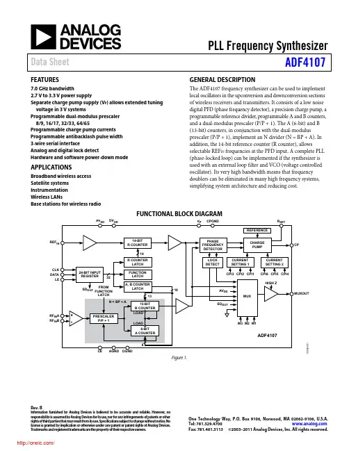
PLL Frequency SynthesizerData SheetADF4107Rev. BInformation furnished by Analog Devices is believed to be accurate and reliable. However , no responsibility is assumed by Analog Devices for its use, nor for any infringements of patents or other rights of third parties that may result from its use. Specifications subject to change without notice. No license is granted by implication or otherwise under any patent or patent rights of Analog Devices. T rademarks and registered trademarks are the property of their respective owners.One Technology Way, P.O. Box 9106, N orwood, MA 02062-9106, U.S.A.Tel: 781.329.4700 Fax: 781.461.3113 ©2003–2011 Analog Devices, Inc. All rights reserved.FEATURES7.0 GHz bandwidth2.7 V to3.3 V power supplySeparate charge pump supply (V P ) allows extended tuning voltage in 3 V systemsProgrammable dual-modulus prescaler 8/9, 16/17, 32/33, 64/65Programmable charge pump currents Programmable antibacklash pulse width 3-wire serial interfaceAnalog and digital lock detectHardware and software power-down modeAPPLICATIONSBroadband wireless access Satellite systems Instrumentation Wireless LANsBase stations for wireless radioGENERAL DESCRIPTIONThe ADF4107 frequency synthesizer can be used to implement local oscillators in the upconversion and downconversion sections of wireless receivers and transmitters. It consists of a low noise digital PFD (phase frequency detector), a precision charge pump, a programmable reference divider, programmable A and B counters, and a dual-modulus prescaler (P/P + 1). The A (6-bit) and B (13-bit) counters, in conjunction with the dual-modulus prescaler (P/P + 1), implement an N divider (N = BP + A). In addition, the 14-bit reference counter (R counter), allowsselectable REF IN frequencies at the PFD input. A complete PLL (phase-locked loop) can be implemented if the synthesizer is used with an external loop filter and VCO (voltage controlled oscillator). Its very high bandwidth means that frequency doublers can be eliminated in many high frequency systems, simplifying system architecture and reducing cost.FUNCTIONAL BLOCK DIAGRAM03338-001CLK DATAREF RF IN RF INFigure 1.ADF4107Data SheetRev. B | Page 2 of 20TABLE OF CONTENTSFeatures..............................................................................................1 Applications.......................................................................................1 General Description.........................................................................1 Functional Block Diagram..............................................................1 Revision History...............................................................................2 Specifications.....................................................................................3 Timing Characteristics................................................................4 Absolute Maximum Ratings............................................................5 ESD Caution..................................................................................5 Pin Configurations and Function Descriptions...........................6 Typical Performance Characteristics.............................................7 Functional Description....................................................................9 Reference Input Stage...................................................................9 RF Input Stage...............................................................................9 Prescaler (P/P + 1)........................................................................9 A and B Counters.........................................................................9 R Counter......................................................................................9 Phase Frequency Detector and Charge Pump..............................9 MUXOUT and Lock Detect......................................................10 Input Shift Register....................................................................10 Latch Summary...........................................................................11 Reference Counter Latch Map..................................................12 AB Counter Latch Map.............................................................13 Function Latch Map...................................................................14 Initialization Latch Map............................................................15 Function Latch............................................................................16 Initialization Latch.....................................................................17 Device Programming after Initial Power-Up.............................17 Applications.....................................................................................18 Local Oscillator for LMDS Base Station Transmitter............18 Interfacing...................................................................................19 PCB Design Guidelines for Chip Scale Package....................19 Outline Dimensions.......................................................................20 Ordering Guide.. (20)REVISION HISTORY9/11—Rev. A to Rev. BChanges to Normalized Phase Noise Floor (PN SYNTH ) Parameter, Table 1................................................................................................3 Added Normalized 1/f Noise (PN 1_f ) Parameter and Endnote 11, Table 1................................................................................................3 Changed EV AL-ADF4107EB1 to EV AL-ADF411xEBZ1............4 Changes to Figure 4 and Table 4.....................................................6 Updated Outline Dimensions.......................................................20 Changes to Ordering Guide. (20)4/07—Rev. 0 to Rev. AUpdated Format..................................................................Universal Changes to REF IN Characteristics Section.....................................3 Changes to Noise Characteristics Section.....................................4 Changes to Absolute Maximum Ratings Section.........................5 Changes to Figure 23......................................................................12 Changes to Ordering Guide. (20)5/03—Revision 0: Initial VersionData SheetADF4107Rev. B | Page 3 of 20SPECIFICATIONSAV DD = DV DD = 3 V ± 10%, AV DD ≤ V P ≤ 5.5 V , AGND = DGND = CPGND = 0 V , R SET = 5.1 kΩ, dBm referred to 50 Ω, T A = T MAX to T MIN , unless otherwise noted. Table 1.Parameter B Version 1 B Chips 2 (Typ) Unit Test Conditions/Comments RF CHARACTERISTICS RF Input Frequency (RF IN )3 1.0/7.0 1.0/7.0 G H z min/max See Figure 18 for input circuit RF Input Sensitivity –5/+5 –5/+5 dBm min/maxMaximum Allowable Prescaler OutputFrequency 4300 300 M H z max REF IN CHARACTERISTICS REF IN Input Frequency 20/250 20/250 MHz min/max For f < 20 MHz, ensure slew rate >50 V/μsREF IN Input Sensitivity 50.8/V DD 0.8/V DD V p-p min/max Biased at AV DD /26 REF IN Input Capacitance 10 10 pF max REF IN Input Current ±100 ±100 μA max PHASE DETECTOR Phase Detector Frequency 7 104 104 MHz max ABP = 0,0 (2.9 ns antibacklash pulse width) CHARGE PUMP Programmable; see Figure 25 I CP Sink/Source High Value 5 5 mA typ With R SET = 5.1 kΩ Low Value 625 625 μA typ Absolute Accuracy 2.5 2.5 % typ With R SET = 5.1 kΩ R SET Range 3.0 to 11 3.0 to 11 kΩ typ See Figure 25 I CP Three-State Leakage 1 1 nA typ Sink and Source Current Matching 2 2 % typ 0.5 V ≤ V CP ≤ V P − 0.5 V I CP vs. V CP 1.5 1.5 % typ 0.5 V ≤ V CP ≤ V P − 0.5 V I CP vs. Temperature 2 2 % typ V CP = V P /2 LOGIC INPUTS V IH , Input High Voltage 1.4 1.4 V min V IL , Input Low Voltage 0.6 0.6 V max I INH , I INL , Input Current ±1 ±1 μA max C IN , Input Capacitance 10 10 pF max LOGIC OUTPUTS V OH , Output High Voltage 1.4 1.4 V min Open-drain output chosen; 1 kΩ pull-upresistor to 1.8 VV OH , Output High Voltage V DD − 0.4 V DD − 0.4 V min CMOS output chosen I OH 100 100 μA max V OL , Output Low Voltage 0.4 0.4 V max I OL = 500 μA POWER SUPPLIES AV DD 2.7/3.3 2.7/3.3 V min/V max DV DD AV DD AV DD V P AV DD /5.5 AV DD /5.5 V min/V max AV DD ≤ V P ≤ 5.5 V I DD 8 (AI DD + DI DD ) 17 15 mA max 15 mA typ I P 0.4 0.4 mA max T A = 25°C Power-Down Mode 9 (AI DD + DI DD ) 10 10 μA typ NOISE CHARACTERISTICSNormalized Phase Noise Floor (PN SYNTH )10−223 −223 dBc/H z typ PLL loop BW = 500 kHz, measured at100 kHz offsetNormalized 1/f Noise (PN 1_f )11 −122 −122 dBc/Hz typ 10 kHz offset; normalized to 1 GHzADF4107Data SheetRev. B | Page 4 of 20Parameter B Version 1 B Chips 2 (Typ) Unit Test Conditions/CommentsPhase Noise Performance 12@ VCO output 900 MHz Output 13 −93 −93 dBc/Hz typ @ 1 kHz offset and 200 kHz PFD frequency6400 MHz Output 14−76 −76 dBc/Hz typ @ 1 kHz offset and 200 kHz PFD frequency6400 MHz Output 15−83 −83 dBc/Hz typ @ 1 kHz offset and 1 MHz PFD frequency Spurious Signals900 MHz Output 13−90/−92 −90/−92 dBc typ @ 200 kHz/400 kHz and 200 kHz PFDfrequency6400 MHz Output 14−65/−70 −65/−70 dBc typ @ 200 kHz/400 kHz and 200 kHz PFDfrequency6400 MHz Output 15 −70/−75 −70/−75 dBc typ @ 1 MHz/2 MHz and 1 MHz PFD frequency1 Operating temperature range (B version) is −40°C to +85°C. 2The B chip specifications are given as typical values. 3Use a square wave for lower frequencies, below the minimum stated. 4This is the maximum operating frequency of the CMOS counters. The prescaler value should be chosen to ensure that the RF input is divided down to a frequency that is less than this value. 5AV DD = DV DD = 3 V. 6AC-coupling ensures AV DD /2 bias. 7Guaranteed by design. Sample tested to ensure compliance. 8T A = 25°C; AV DD = DV DD = 3 V; P = 32; RF IN = 7.0 GHz. 9T A = 25°C; AV DD = DV DD = 3.3 V; R = 16,383; A = 63; B = 891; P = 32; RF IN = 7.0 GHz. 10The synthesizer phase noise floor is estimated by measuring the in-band phase noise at the output of the VCO and subtracting 20logN (where N is the N divider value) and 10 log(F PFD ). PN SYNTH = PN TOT – 20 logN −10 logF PFD . 11The PLL phase noise is composed of 1/f (flicker) noise plus the normalized PLL noise floor. The formula for calculating the 1/f noise contribution at an RF frequency, f RF , and at a frequency offset, f, is given by PN = PN 1_f + 10 log(10 kHz/f) + 20 log(f RF /1 GHz). Both the normalized phase noise floor and flicker noise are modeled in ADIsimPLL. 12The phase noise is measured with the EVAL-ADF411xEBZ1 evaluation board and the HP8562E spectrum analyzer. The spectrum analyzer provides the REF IN for the synthesizer (f REFOUT = 10 MHz @ 0 dBm). 13f REFIN = 10 MHz; f PFD = 200 kHz; offset frequency = 1 kHz; f RF = 900 MHz; N = 4500; loop BW = 20 kHz. 14f REFIN = 10 MHz; f PFD = 200 kHz; offset frequency = 1 kHz; f RF = 6400 MHz; N = 32,000; loop BW = 20 kHz. 15f REFIN = 10 MHz; f PFD = 1 MHz; offset frequency = 1 kHz; f RF = 6400 MHz; N = 6400; loop BW = 100 kHz.TIMING CHARACTERISTICSAV DD = DV DD = 3 V ± 10%, AV DD ≤ V P ≤ 5.5 V , AGND = DGND = CPGND = 0 V , R SET = 5.1 kΩ, dBm referred to 50 Ω, T A = T MAX to T MIN , unless otherwise noted. 1 Table 2.Parameter Limit 2 (B Version) UnitTest Conditions/Comments t 1 10 ns min DATA to CLOCK setup time t 2 10 ns min DATA to CLOCK hold time t 3 25 ns min CLOCK high duration t 4 25 ns min CLOCK low duration t 5 10 ns minCLOCK to LE setup time t 6 20ns min LE pulse width1 Guaranteed by design but not production tested.2Operating temperature range (B Version) is −40°C to +85°C.03338-002CLOCKDATALELEFigure 2. Timing DiagramData SheetADF4107Rev. B | Page 5 of 20ABSOLUTE MAXIMUM RATINGST A = 25°C, unless otherwise noted.Table 3. Parameter Rating AV DD to GND 1−0.3 V to +3.6 V AV DD to DV DD −0.3 V to +0.3 V V P to GND −0.3 V to +5.8 V V P to AV DD −0.3 V to +5.8 VDigital I/O Voltage to GND −0.3 V to V DD + 0.3 VAnalog I/O Voltage to GND −0.3 V to V p + 0.3 VREF IN , RF IN A, RF IN B to GND −0.3 V to V DD + 0.3 VOperating Temperature RangeIndustrial (B Version) −40°C to +85°C Storage Temperature Range −65°C to +125°CMaximum Junction Temperature 150°C TSSOP θJA Thermal Impedance 112°C/W LFCSP θJA Thermal Impedance (Paddle Soldered)30.4°C/W Reflow SolderingPeak Temperature 260°CTime at Peak Temperature 40 secTransistor CountCMOS 6425 Bipolar 3031GND = AGND = DGND = 0 V.Stresses above those listed under Absolute Maximum Ratings may cause permanent damage to the device. This is a stressrating only; functional operation of the device at these or any other conditions above those indicated in the operationalsection of this specification is not implied. Exposure to absolute maximum rating conditions for extended periods may affect device reliability. This device is a high performance RF integrated circuit with anESD rating of <2 kV , and it is ESD sensitive. Proper precautionsshould be taken for handling and assembly.ESD CAUTIONADF4107Data SheetRev. B | Page 6 of 20PIN CONFIGURATIONS AND FUNCTION DESCRIPTIONS03338-003R SET CP CPGND AGNDRF IN B RF IN A AV DD REF IN MUXOUTLE DATA CLKCE DGNDV P DV DD NOTES:1. TRANSISTOR COUNT 6425 (CMOS), 303 (BIPOLAR).Figure 3. Pin Configuration, TSSOP 03338-004CPGND 1AGND 2AGND 320 C P 6 7 8D G N D 9D G N D 1019181716RF IN B 4RF IN A 5R S E T V P D V D D D V D DA V D D A V D D R E F I N NOTES:1. TRANSISTOR COUNT 6425 (CMOS), 303 (BIPOLAR).2. THE EXPOSED PAD MUST BE CONNECTED TO AGND.Figure 4. Pin Configuration, LFCSPData SheetADF4107Rev. B | Page 7 of 20TYPICAL PERFORMANCE CHARACTERISTICS03338-005Figure 5. Parameter Data for the RF Input–30–10–25–20–1503338-006RF INPUT FREQUENCY (GHz)R F I N P U T P O W E R (d B m )Figure 6. Input Sensitivity–100–90–80–70–60–50–40–30–20–1003338-007–2kHz–1kHz900MHz 1kHz2kHzFREQUENCYO U T P U T P O W E R (d B )Figure 7. Phase Noise (900 MHz, 200 kHz, 20 kHz) –40–140–130–120–110–100–90–80–70–60–5003338-008100Hz1MHzFREQUENCY OFFSET FROM 900MHz CARRIERP H A S E N O I S E (d B c /H z )Figure 8. Integrated Phase Noise (900 MHz, 200 kHz, 20 kHz)–100–90–80–70–60–50–40–30–20–1003338-009–400kHz–200kHz900MHz 200kHz400kHzFREQUENCYO U T P U T P O W E R (d B )Figure 9. Reference Spurs (900 MHz, 200 kHz, 20 kHz)–100–90–80–70–60–50–40–30–20–1003338-010–2kHz–1kHz6400MHz 1kHz2kHzFREQUENCYO U T P U T P O W E R (d B )Figure 10. Phase Noise (6.4 GHz, 1 MHz, 100 kHz)ADF4107Data SheetRev. B | Page 8 of 20–40–140–130–120–110–100–90–80–70–60–5003338-011100Hz1MHzFREQUENCY OFFSET FROM 5800MHz CARRIERP H A S E N OI S E (d B c /H z )Figure 11. Integrated Phase Noise (6.4 GHz, 1 MHz, 100 kHz)–10003338-012–2kHz –1kHz 5800MHz 1kHz 2kHzFREQUENCY (MHz)O U T P U T P O W E R (d B )Figure 12. Reference Spurs (6.4 GHz, 1 MHz, 100 kHz)–60–100–90–80–703338-013TEMPERATURE (°C)P H A S E N O I S E (d B c /H z )Figure 13. Phase Noise (6.4 GHz, 1 MHz, 100 kHz) vs. Temperature –5–105–95–85–75–65–55–45–35–25–1503338-014501234TUNING VOLTAGE (V)F I R S T R E F E R E N C E S P U R (d B c )Figure 14. Reference Spurs vs. V TUNE (6.4 GHz, 1 MHz, 100 kHz)–120–180–170–160–150–140–13003338-015100M10k100k 1M 10M PHASE DETECTOR FREQUENCY (Hz)P H A S E N O I S E (d B c /H z )V DD = 3V V P = 5VFigure 15. Phase Noise (Referred to CP Output) vs. PFD Frequency03338-016V CP (V)I C P (m A )Figure 16. Charge Pump Output CharacteristicsData SheetADF4107Rev. B | Page 9 of 20FUNCTIONAL DESCRIPTIONREFERENCE INPUT STAGEThe reference input stage is shown in Figure 17. SW1 and SW2 are normally closed switches. SW3 is normally open. When power-down is initiated, SW3 is closed and SW1 and SW2 are opened. This ensures that there is no loading of the REF IN pin on power-down.03338-017POWER-DOWN CONTROLFigure 17. Reference Input StageRF INPUT STAGEThe RF input stage is shown in Figure 18. It is followed by a 2-stage limiting amplifier to generate the CML clock levels needed for the prescaler.03RF IN RF IN Figure 18. RF Input StagePRESCALER (P/P + 1)The dual-modulus prescaler (P/P + 1), along with the A and B counters, enables the large division ratio, N, to be realized (N = BP + A). The dual-modulus prescaler, operating at CML levels, takes the clock from the RF input stage and divides itdown to a manageable frequency for the CMOS A and CMOS B counters. The prescaler is programmable. It can be set in software to 8/9, 16/17, 32/33, or 64/65. It is based on asynchronous 4/5 core. A minimum divide ratio is possible for fully contiguous output frequencies. This minimum isdetermined by P , the prescaler value, and is given by: (P 2 − P).A ANDB COUNTERSThe A and B CMOS counters combine with the dual-modulus prescaler to allow a wide ranging division ratio in the PLL feedback counter. The counters are specified to work when the prescaler output is 300 MHz or less. Thus, with an RF input frequency of 4.0 GHz, a prescaler value of 16/17 is valid but a value of 8/9 is not valid.Pulse Swallow FunctionThe A and B counters, in conjunction with the dual-modulus prescaler, make it possible to generate output frequencies that are spaced only by the reference frequency divided by R. The equation for the VCO frequency is as follows:()[]Rf A B P f REFINVCO ×+×= where:f VCO is the output frequency of external voltage controlled oscillator (VCO).P is the preset modulus of dual-modulus prescaler (8/9, 16/17). B is the preset divide ratio of binary 13-bit counter (3 to 8191). A is the preset divide ratio of binary 6-bit swallow counter (0 to 63). f REFIN is the external reference frequency oscillator.FROM RF INPUT STAGE03338-019Figure 19. A and B CountersR COUNTERThe 14-bit R counter allows the input reference frequency to be divided down to produce the reference clock to the phasefrequency detector (PFD). Division ratios from 1 to 16,383 are allowed.PHASE FREQUENCY DETECTOR AND CHARGE PUMPThe phase frequency detector (PFD) takes inputs from the R counter and N counter (N = BP + A) and produces an output proportional to the phase and frequency difference between them. Figure 20 is a simplified schematic. The PFD includes a programmable delay element that controls the width of theantibacklash pulse. This pulse ensures that there is no dead zone in the PFD transfer function and minimizes phase noise and reference spurs. Two bits in the reference counter latch, ABP2 and ABP1, control the width of the pulse. Use of the minimum antibacklash pulse width is not recommended. See Figure 23.ADF4107Data SheetRev. B | Page 10 of 20CPV P03338-020Figure 20. PFD Simplified Schematic and Timing (in Lock)MUXOUT AND LOCK DETECTThe output multiplexer on the ADF4107 allows the user to access various internal points on the chip. The state ofMUXOUT is controlled by M3, M2, and M1 in the function latch. Figure 25 shows the full truth table. Figure 21 shows the MUXOUT section in block diagram form.Lock DetectMUXOUT can be programmed for two types of lock detect: digital lock detect and analog lock detect.Digital lock detect is active high. When the lock detectprecision (LDP) bit in the R counter latch is set to 0, digital lock detect is set high when the phase error on three consecutive phase detector (PD) cycles is less than 15 ns. With LDP set to 1, five consecutive cycles of less than 15 ns are required to set the lock detect. It stays set high until a phase error of greater than 25 ns is detected on any subsequent PD cycle.The N-channel open-drain analog lock detect should be operated with an external pull-up resistor of 10 kΩ nominal. When lock has been detected, this output becomes high with narrow, low going pulses.03338-021Figure 21. MUXOUT CircuitINPUT SHIFT REGISTERThe ADF4107 digital section includes a 24-bit input shiftregister, a 14-bit R counter, and a 19-bit N counter, comprising a 6-bit A counter and a 13-bit B counter. Data is clocked into the 24-bit shift register on each rising edge of CLK. The data is clocked in MSB first. Data is transferred from the shift register to one of four latches on the rising edge of LE. The destination latch is determined by the state of the two control bits (C2, C1) in the shift register. These are the two LSBs, DB1 and DB0, as shown in the timing diagram of Figure 2. The truth table for these bits is shown in Table 5. Figure 22 shows a summary of how the latches are programmed. Table 5. C2, C1 Truth TableControl BitsC2 C1 Data Latch 0 0 R Counter 0 1 N Counter (A and B) 1 0 Function Latch (Including Prescaler) 1 1 Initialization Latch分销商库存信息:ANALOG-DEVICESADF4107BRUZ ADF4107BCPZ-REEL ADF4107BRUZ-REEL ADF4107BCPZ-REEL7ADF4107BRUZ-REEL7ADF4107BRU-REEL ADF4107BRU-REEL7ADF4107BRU ADF4107BCPZ。
LED日光灯设计方案日光灯作为一种光亮柔和而有效的光源在全世界广受欢迎,无论是在家居、商店、办公室、学校、超市、医院、剧场,还是在商业冰柜、广告灯箱、地铁、人行隧道、人防工程、夜市灯饰照明等,只要需要照明的地方均可见到日光灯。
传统的荧光日光灯其电源的利用率并不理想:附加镇流器功耗较大,开启时需要辅助高压;日光灯管内置的水银在废弃时无法处理,成为污染环境的公害。
日光灯管的荧光粉在充入日光灯管过程中,含有较多量的汞(水银),因此日光灯管破裂后,跑出来的水银蒸气对人体的危害较大。
权威资料显示:汞蒸气达至3毫克时会使人在2至3月内慢性中毒,达至毫克时会诱发急性汞中毒,如若其量达到20毫克,会直接导致动物死亡。
作为第四代新型节能光源,LED光源诞生之时即被用来做各类灯具的发光光源。
的白光LED草帽灯、食人鱼是最早被用在LED日光灯的发光灯条上的。
每个LED日光灯管使用数量不等,约280-360颗。
现在新一代的LED日光灯发光灯条使用从到1W、显色为纯白、青白、暖白、冷白的贴片LED平面光源。
节能省电是LED日光灯的最大特点。
以T8日光灯为例,标称36W的荧光日光灯(CFL),其附加镇流器耗电8W,工作时实际耗电44W,照亮流明为420lm,使用寿命3千小时。
而同样规格的LED日光灯,工作时实际耗电仅16W,照亮流明为550lm,使用寿命可达3万小时。
PWM LED驱动控制器PT4107LED日光灯的LED灯条电源驱动方案有很多种,目前非隔离方案因其效率高而占主流,而用PWM LED驱动控制器来做LED日光灯驱动电源的又占绝大多数。
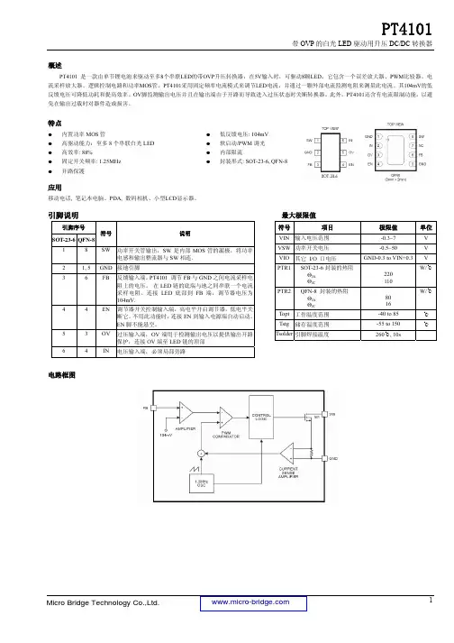
PT4107是一个典型的PWM LED驱动控制器,其内部拓扑结构如图1。
PT4107是一款高压降压式PWM LED驱动控制器,通过外部电阻和内部的齐纳二极管,可以将经过整流的110V或220V交流电压箝位于20V。
当Vin上的电压超过欠压闭锁阈值18V 后,芯片开始工作,按照峰值电流控制的模式来驱动外部的MOSFET。

说明:
本表格是专门为PT4107系统设计的。
后面提供3种典型应用的近似设计方案,用户可以在相近的方案上修改以实现自己的方案。
本方案是一种近似的理想方案,为用户提供参考,最后还是要依据用户具体方案的实际测试结果为准。
220V AC
序号器件参数10功率电阻100K / 2W 11陶瓷电容1uF / 40V 12热敏电阻10K / 保护13
控制芯片PT41071%
0.25 欧姆1A 0.33 欧姆750mA 0.71 欧姆350mA 1%300K 100k Hz 1.2M 25K Hz
LED 个数很少
16MOSFET 2N60680uH 1A 1000uH 750mA 2000uH 350mA
18快速恢复二极管
1A / 500V
19LED 灯20
滤波电容
取决灯的个数(Optional)
110V AC
序号器件参数10
功率电阻47K / 1W 说明
75,82,91,110K
说明36-56K
14采样电阻频率设定电阻电感1715Fosc=100KHz
方案。
体方案的实际测试结果为准。
序号
器件参数20整流桥600V/1A 21热敏电阻400欧姆22高压电容22uF/400V 23高压电容22uF/400V 说明
取决输入输出电压电流取决输入输出电压电流
电解高频
很少。