摩托罗拉Z3(原理图框图PCB)
- 格式:pdf
- 大小:151.72 KB
- 文档页数:3
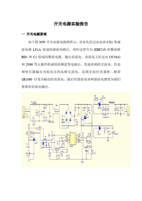
开关电源实验报告一开关电源原理如下图30W开关电源电路图所示,市电先经过由电容CX1和滤波电感LF1A组成的滤波电路后,再经过型号为KBP210的整流桥BD1和C1组成的整流电路,输出直流电。
直流电又经过由UC3842和2N60等元器件组成的高频逆变电路后,变成高频的交流电,经高频变压器输出为低电压的高频交流电。
高频交流经肖基特二极管SR1060后变为脉动的直流电,最后经滤波电容和滤波电感变为我们想要的直流电输出。
MOV2、MOV3:F1、F2、F3、FDG1组成的电路进行保护。
当加在压敏电阻两端的电压超过其工作电压时,其阻值降低,使高压能量消耗在压敏电阻上,若电流过大,F1、F2、F3会烧毁保护后级电路。
(2)输入滤波电路:C1、L1、C2、C3组成的双π型滤波网络主要是对输入电源的电磁噪声及杂波信号进行抑制,防止对电源干扰,同时也防止电源本身产生的高频杂波对电网干扰。
当电源开启瞬间,要对C5充电,由于瞬间电流大,加RT1(热敏电阻)就能有效的防止浪涌电流。
因瞬时能量全消耗在RT1电阻上,一定时间后温度升高后RT1阻值减小(RT1是负温系数元件),这时它消耗的能量非常小,后级电路可正常工作。
(3)整流滤波电路:交流电压经BRG1整流后,经C5滤波后得到较为纯净的直流电压。
若C5容量变小,输出的交流纹波将增大。
1.2功率变换电路(1)MOS管的工作原理:目前应用最广泛的绝缘栅场效应管是MOSFET(MOS管),是利用半导体表面的电声效应进行工作的。
也称为表面场效应器件。
由于它的栅极处于不导电状态,所以输入电阻可以大大提高,最高可达105欧姆,MOS管是利用栅源电压的大小,来改变半导体表面感生电荷的多少,从而控制漏极电流的大小。
(2)常见的原理图:(3)工作原理R4、C3、R5、R6、C4、D1、D2组成缓冲器,和开关MOS管并接,使开关管电压应力减少,EMI减少,不发生二次击穿。
在开关管Q1关断时,变压器的原边线圈易产生尖峰电压和尖峰电流,这些元件组合一起,能很好地吸收尖峰电压和电流。
摩托罗拉Droid3全程拆解MOTO近日发布了令人期待的Droid3。
为使更多发烧友们能更好了解这款机型,第一步1. Droid 2经历了几代升级和特别版之后,今天终于更新换代了!摩托罗拉第三代Droid的正式定名为Droid 3。
2. 距离第一代Droid推出市场已经有两年了,摩托罗拉对Droid 3进行了全面技术升级。
l Android 2.3操作系统l Dual-Core 1GHz处理器l 5行标准键盘l 8百万像素摄像头,1080p高清摄录l 4″ 960 x 540高清显示屏,Gorilla Glass玻璃技术第二步1. 摩托罗拉表示,Droid 3是“史上最薄的全键盘智能手机”。
与原版Droid相比,Droid 3确实较为小巧,但薄了多少却不明显。
2. 背面摄像头包括LED闪光灯和8倍变焦。
3. Droid 3支持micro USB和micro HDMI插口,支持1080p视频直接输出。
插口位于Droid 3的左侧,与摩托罗拉的Atrix异曲同工。
第三步1. 打开后盖,可以看到可更换电池。
2. 摩托罗拉表示,Droid 3待机时间为300小时,可连续通话9小时。
3. 我们怀疑,待机300小时也太无趣了。
电池为3.7V 1540毫安。
第四步1. 这款Droid有SIM卡。
Verizon 的网络协议CDMA不需要SIM卡。
2. 没有SIM卡严重影响到Verizon网络的全球使用。
包含了SIM卡意味着Droid 3可以全球通用。
第五步1. 与前代一样,Droid 3是由T5内梅花头螺钉固定。
2. 摩托罗拉喜欢将螺钉和插销藏在信息标签下面,需要揭掉才能看见,当然这些只是小意思,难不倒专业的我们了。
3. 将螺钉、夹子和贴纸都取下以后,我们看到了Droid 3内部全貌。
第六步1. 接下来,我们使用塑料片将摄像头带状电缆从主板上剥离。
2. Droid 3背面装有800万像素摄像头,可以进行30 fps、1080p录像。

PCB变形的建模与仿真----印刷电路板在回焊过程中变形的建模与仿真摘要在SMT中,回焊是非常重要的工站。
在回焊过程中受到热冲击已成为印刷电路板(简称为PCB)组件生产过程中产生缺陷的主要原因之一。
PCB组件组成材料不同,热膨胀系数等热性能参数相差较大,容易产生翘曲变形等缺陷,造成元器件和PCB之间的电气和物理连接失败,导致整个PCB组件失效。
而由于传统的,经反复试验、反复调整来改进回焊工艺的方法既费时又耗费大量实验经费,不能适应当前电子产品更新速度快、竞争日益激烈的需求,在这一背景下,焊接工艺的建模与仿真、预测与控制研究引起了广泛的关注。
模拟仿真可以识别在回焊过程中的温度变化以及确定其对生产质量的影响;对回焊温度曲线的设定使设计者根据PCB热分布重新排布组件从而使产品设计达到最优化。
本文利用有限元法对PCB组件在回焊过程中的受热进行分析,建立瞬态温度场和应力场模型。
用ANSYS软件对PCB组件在回焊过程中由于受热产生的热机械反应进行了模拟和建模,得出了温度场以及应力场的分布。
由于PCB组件组成材料的热物理性能不同,以及经过不同的温区加热,模拟了不同时刻整个PCB组件的温度场分布。
建立了一个贴装了3个PLCC的4层PCB板物理简化模型,模拟了在三种约束条件下,该组件在回焊过程中受热冲击时,产生的热应力及热变形。
选取PCB上3个点,得到了在三种约束下面位移和离面位移的位移量,即在底面对角两点约束下面位移和离面位移的位移量最大;底面4顶点约束下面位移和离面位移的位移量其次;底面两对边约束下面位移和离面位移的位移量最小。
通过仿真可对回焊温度曲线进行优化,使得PCB 组件得到比较均匀的温度场分布,并调整对PCB的约束,使得变形最小化。
关键词:回焊;热应力;建模;温度场;仿真;,Modelling and simulating for PCB Deformedin refolw solderingAbstract of thesisReflow soldering is very important technics in SMT. Thermal impact to PCBA during reflow soldering is considered one of the main drivers for manufacturing defects. The materials making up a PCBA is various, and the thermal property of the materials is also different ,this may cause some defects for example wargpage. Excessive warpage in the PCB may result in gaps forming between the module leads and the molten solder on the solder pads, then the failure of electronically and physical connection lead to PCBA's defect. The traditional approach of experimentally analysing production defects would be costly and virtually impossible, and can't reach the demand of the producer for the fast renovation and the acute competition. An alternative to this approach is to derive computational and numerical models that encapsulate representations of the key process physics, so that effect analysis of the pertinent process variables may be examined. The application of the modelling and simulation to a sample PCBA has been carried out to explore how undue variations in the reflow temperature can be minimized by a number of different strategies. It has been shown that simple movements of components can have quite beneficial effects on the overall process thermal history of the PCB.The paper use finite element analysis method analysis the thermal impact of PCBA during the reflow soldering ,and building the temperature and stress distribution model. The paper model and simulate the thermal warpage of PCBA during reflow soldering , get the temperature and stress distribution of PCBA. This paper simulate the temperature distribution of PCBA under the condition of the material making up PCBA is different ,and PCBA will go through different oven section, building a simple physical model of a 4-layer PCB with 3 PLCCs to simulate the thermal stress and warpage of PCBA under three constrained conditions, when the PCBA go through the oven sections. Compared the surface displacement and the Zaxis displacement of three points on the PCB under the three constrained condition to get the result of following. The thermal warpage happened under the constrained conditions of the two points on the cross were constrained is large than that happened under the constrained conditions of the four points were constrained . the constrained conditions of the two sides were Simulation warpage is constrained. Optimize and the temperature minimized by adjusting,the temperature figure is attainable through the distribution of PCBA is more uniform, also the constrained condition.KEYWORD: refolw soldering; thermal stress; modeling temperature field; Simulation;1目录摘要 (1)Abstract (1)目录 (2)第一章绪论 (3)1.课题背景意义.................................................................................................................32.国内外研究概况 (3)3.研究思路及方法 (4)第二章PCB组件概述 (5)2.1 PCB简介 (5)2.1.1 PCB的分类 (5)2.1.2 PCB的材料组成 (6)2.1.3 PCB的制造流程 (7)2.2 PCB组件 ....................................................................................................................... .82.3 小结 (8)第三章PCB理论分析与建模 (12)3.1温度场数学模型的建立 (12)3.1.1温度场概况 (12)3.1.2热传递的基本方式 (12)3.1.3初始条件和边界条件 (13)3.1.4温度场的泛函表达式 (15)3.2热应力的数学模型 (19)3.2.1 热应力概述 ........................................................................................................193.2.2 热弹性理论基本方程 (20)23.2.3 热应力的有限元方程.......................................................................................223.3 小结 (23)第四章PCB组件的建模与仿真 (24)4.1 建模以及仿真步骤 (24)4.2 仿真结果及分析 (4)24.3 小结 (4)4第五章:总结与展望 (4)5致谢 (46)参考文献 (4)7附录 (4)8第一章绪论1.课题背景及意义在SMT中,回焊是非常重要的工站。
说明:1.本报告必须由承担毕业设计(论文)课题任务的学生在接到“毕业设计(论文)任务书”、正式开始做毕业设计(论文)的第2周或第3周末之前独立撰写完成,并交指导教师审阅。
2.每个毕业设计(论文)课题撰写本报告一份,作为指导教师、教研室主任审查学生能否承担该毕业设计(论文)课题任务的依据,并接受学校的抽查。
中文摘要电源是各种电子设备的核心,它有如人体的心脏,是所有电类设备的动力。
20世纪90年代以来,随着电力电子技术飞速地发展,不断涌现出新型电力电子器件,高智商化IC和新电路拓扑,创造出十年前意想不到的许多新型稳压电源。
现代高频开关稳压电源作为电源的一个分支,由于它具有功率小,效率高,体积小,重量轻,稳压范围宽,可靠安全等一系列特点,现在正越来越受到青睐和推崇。
现代高频开关稳压电源技术涉及的内容是极其广泛和复杂的,它横跨了三个学科:一是微电子精细加工的智能化专用集成电路控制芯片系统;二是正在快速更新的高性能功率半导体MOSFET和IGBT等电力电子器件;三是要合理利用,绕制各种电感器件和变压器所用的磁性材料等几大类。
现代开关稳压电源已广泛用于基础直流电源,交流电源,各种工业电源,计算机电源,UPS不间断电源,医疗和照明电源,雷达高压电源,音响和视频电源等。
本文设计的单相脉宽调制逆变电源属于交流电源(AC-DC-AC逆变),采用电压反馈控制,通过中断功率通量和调节占空比的方法来改变驱动电压脉冲宽度来调整和稳定输出电压。
其主电路构成采用的是Boost电路和全桥电路的组合。
控制电路采用了2片集成脉宽调制电路芯片,一片用来产生PWM波,另一片与正弦函数发生芯片做适当的连接来产生SPWM波,集成芯片比分立元器件控制电路具有更简单,更可靠的特点和易于调试的优点。
本文详细的分析了该逆变电源的工作过程,并推导了重要公式。
最后对该逆变电源进行了计算机仿真和样机实验,验证了其可行性和有效性。
关键词:逆变器;正弦脉宽调制;场效应管AbstractPower supply is core and drive of electric equipments. With the flying development of power electronics technology, It has come forth continually that is IC of high intelligence, new type electronic device and topology since 1990's. As aresult, A lot of new type steady-voltage power supply has been created that is indescribable ten years ago. High-frequency switching power supply is a branch of power supply. It possesses many advantages such as low-power, high-frequency, small- volume, light-weight, wide-range of steady voltage, credibility and security. It has been received and upheld by the people. It involves a great deal content that is extensive and intricate. It bestrides subject of three aspects. The first is IC control chip system of micro-electronics; The second is electronic devices of high-performance power semiconductor such as MOSFET and IGBT. The third is various devices of inductance and magnetic materials of transformer how to be utilized and rolled rationally.Steady voltage power supply of modern switching has been applied in the following aspects widely. They are DC power supply, AC power supply, industry power supply, computer power supply, UPS power supply, power supply of medical treatment and lighting, high voltage power supply of radar, power supply of sound and video frequency and so on. Single-phase Sinusoidal Pulse Width Modulation Inverter Power Supply in this paper belongs to AC power supply (AC-DC-AC convert). Control mode adopts feedback of voltage control. The methods of intermitting power flux and changing duty-cycle can change pulse width of drive voltage that adjust and rectify output voltage ultimately. The main circuit is made up of compounding of Boost and the full-bridge circuit. The control circuit adopts two chips of integrated pulse width modulation. One produces PWM waveform. The other connects chip of producing sinusoidal signal properly, which brings SPWM waveform. Integrated chip is more simple, reliable and laboratorial than discrete component.The operation of inverter power supply is thoroughly analyzed and some important formulas are deduced. Finally, the principle of operation are illustrated and verified on emulation and experimental results.Key words: inverter; Sinusoidal Pulse Width Modulation,MOSFET目录第1章概述 (1)1.1现代电源发展概况 (1)1.1.1 交流稳压电源 (1)1.1.2 UPS及交流净化电源 (2)1.1.3 工业电源的发展 (2)1.1.4 直流开关电源 (2)1.1.5 软开关——PWM功率变换器 (3)1.1.6 分布电源技术的发展 (4)1.1.7 功率因数校正技术 (4)第2章 PWM的工作原理 (5)2.1 PWM的基本原理 (5)2.2 PWM型逆变电路的控制方式 (8)2.2.1 异步调制 (8)2.2.2 同步调制 (9)2.3 SPWM波形的生成方法 (9)第3章逆变电源组成及主电路的设计 (10)3.1 系统组成 (10)3.2 主电路组成及工作原理 (11)3.3 主电路设计 (11)3.3.1 共模抑制环节 (11)3.3.2 工频变压器设计 (13)3.3.3 限流电路设计 (14)3.3.4 Boost变换器设计 (15)3.3.5 桥式逆变器基本原理 (20)3.4 主电路图 (21)第4章逆变电路的控制电路设计 (22)4.1 辅助电源设计 (22)4.2 控制电路框图 (23)4.3 SG3524和ICL8038芯片介绍 (24)4.3.1 SG3524芯片 (24)4.3.2 ICL8038芯片 (25)4.4 控制电路设计 (27)4.4.1 利用SG3524生成SPWM波形 (27)4.4.2 驱动电路设计 (28)4.4.2.1 驱动电路工作原理 (28)4.4.2.2 驱动电路参数原理图 (29)4.4.3 过流保护电路 (30)4.4.4 反馈调压电路 (30)4.4.4.1 反馈调压电路工作原理 (30)4.4.4.2 反馈调压电路主电路图 (31)4.5 控制电路图 (32)第5章结论与展望 (33)致谢 (34)参考文献 (36)第1章概述1.1 现代电源发展概况现代电源技术是综合应用了电力电子、电子与电磁技术、自动控制及微处理器技术的一种多学科技术。