98C64A写入时序
- 格式:doc
- 大小:34.00 KB
- 文档页数:1

64 Kb I2C CMOS Serial EEPROMCAT24C64DescriptionThe CAT24C64 is a 64 Kb CMOS Serial EEPROM device, internally organized as 8192 words of 8 bits each.It features a 32−byte page write buffer and supports the Standard (100 kHz), Fast (400 kHz) and Fast−Plus (1 MHz) I2C protocol. External address pins make it possible to address up to eight CAT24C64 devices on the same bus.Features•Supports Standard, Fast and Fast−Plus I2C Protocol•1.7 V to 5.5 V Supply V oltage Range•32−Byte Page Write Buffer•Hardware Write Protection for Entire Memory•Schmitt Triggers and Noise Suppression Filters on I2C Bus Inputs (SCL and SDA)•Low Power CMOS Technology•1,000,000 Program/Erase Cycles•100 Year Data Retention•Industrial and Extended Temperature Range•SOIC, TSSOP, UDFN 8−pad and Ultra−thin WLCSP 4−bump Packages•This Device is Pb−Free, Halogen Free/BFR Free, and RoHS CompliantFigure 1. Functional Symbol SDASCL WPV CC SSA2, A1, APIN CONFIGURATIONS (Top Views)See detailed ordering and shipping information in the package dimensions section on page 8 of this data sheet.ORDERING INFORMATIONSOIC−8W SUFFIXCASE 751BDSOIC (W), TSSOP (Y),UDFN (HU4)Y SUFFIXCASE 948ALDevice AddressA0, A1, A2Serial DataSDASerial ClockSCLWrite ProtectWPPower SupplyV CCGroundV SSFunctionPin NamePIN FUNCTIONFor the location of Pin 1, please consult thecorresponding package drawing.UDFN−8HU4 SUFFIXCASE 517AZWLCSP−4C4C SUFFIXCASE 567JYSDAWPV CCV SSA2A1A01SCLWLCSPA1A2B1B2SDAV SSSCLV CC1X= Specific Device Code(see ordering information)Y= Production Year (Last Digit)M= Production Month (1−9, O, N, D)W= Production Week CodeMARKINGDIAGRAMS(WLCSP−4)WLCSP−4C4U SUFFIXCASE 567PBXYM(C4C)For serial EEPROM in a US8 package, pleaseTable 1. ABSOLUTE MAXIMUM RATINGSParameters Ratings Units Storage Temperature–65 to +150°C Voltage on Any Pin with Respect to Ground (Note 1)–0.5 to +6.5V Stresses exceeding those listed in the Maximum Ratings table may damage the device. If any of these limits are exceeded, device functionality should not be assumed, damage may occur and reliability may be affected.1.The DC input voltage on any pin should not be lower than −0.5 V or higher than V CC + 0.5 V. During transitions, the voltage on any pin mayundershoot to no less than −1.5 V or overshoot to no more than V CC + 1.5 V, for periods of less than 20 ns.Table 2. RELIABILITY CHARACTERISTICS (Note 2)Symbol Parameter Min UnitsN END (Note 3)Endurance1,000,000Program/Erase Cycles T DR Data Retention100Years2.These parameters are tested initially and after a design or process change that affects the parameter according to appropriate AEC−Q100and JEDEC test methods.3.Page Mode, V CC = 5 V, 25°C.Table 3. D.C. OPERATING CHARACTERISTICS(V CC = 1.8 V to 5.5 V, T A = −40°C to +125°C and V CC = 1.7 V to 5.5 V, T A = −40°C to +85°C, unless otherwise specified.)Symbol Parameter Test Conditions Min Max UnitsI CCR Read Current Read, f SCL = 400 kHz1mAI CCW Write Current Write, f SCL = 400 kHz2mAI SB Standby Current All I/O Pins at GND or V CC T A = −40°C to +85°CV CC≤ 3.3 V1m AT A = −40°C to +85°CV CC > 3.3 V3T A = −40°C to +125°C5I L I/O Pin Leakage Pin at GND or V CC2m AV IL Input Low Voltage−0.5V CC x 0.3V V IH Input High Voltage V CC x 0.7V CC + 0.5V V OL1Output Low Voltage V CC≥ 2.5 V, I OL = 3.0 mA0.4V V OL2Output Low Voltage V CC < 2.5 V, I OL = 1.0 mA0.2V Table 4. PIN IMPEDANCE CHARACTERISTICS(V CC = 1.8 V to 5.5 V, T A = −40°C to +125°C and V CC = 1.7 V to 5.5 V, T A = −40°C to +85°C, unless otherwise specified.) Symbol Parameter Conditions Max UnitsC IN (Note 4)SDA I/O Pin Capacitance V IN = 0 V8pFC IN (Note 4)Input Capacitance (other pins)V IN = 0 V6pFI WP (Note 5)WP Input Current V IN < V IH, V CC = 5.5 V130m AV IN < V IH, V CC = 3.3 V120V IN < V IH, V CC = 1.8 V80V IN> V IH2I A (Note 5)Address Input Current(A0, A1, A2)Product Rev F V IN < V IH, V CC = 5.5 V50m A V IN < V IH, V CC = 3.3 V35V IN < V IH, V CC = 1.8 V25V IN> V IH24.These parameters are tested initially and after a design or process change that affects the parameter according to appropriate AEC−Q100and JEDEC test methods.5.When not driven, the WP, A0, A1 and A2 pins are pulled down to GND internally. For improved noise immunity, the internal pull−down is relativelystrong; therefore the external driver must be able to supply the pull−down current when attempting to drive the input HIGH. T o conserve power, as the input level exceeds the trip point of the CMOS input buffer (~ 0.5 x V CC), the strong pull−down reverts to a weak current source.Table 5. A.C. CHARACTERISTICS(V CC = 1.8 V to 5.5 V, T A = −40°C to +125°C and V CC = 1.7 V to 5.5 V, T A = −40°C to +85°C.) (Note 6)Symbol ParameterStandardV CC = 1.7 V − 5.5 VFastV CC = 1.7 V − 5.5 VFast−PlusV CC = 1.7 V − 5.5 VT A = −405C to +855CUnits Min Max Min Max Min MaxF SCL Clock Frequency1004001,000kHzt HD:STA START Condition Hold Time40.60.25m s t LOW Low Period of SCL Clock 4.7 1.30.45m s t HIGH High Period of SCL Clock40.60.40m s t SU:STA START Condition Setup Time 4.70.60.25m s t HD:DAT Data In Hold Time000m s t SU:DAT Data In Setup Time25010050ns t R (Note 7)SDA and SCL Rise Time1,000300100ns t F (Note 7)SDA and SCL Fall Time300300100ns t SU:STO STOP Condition Setup Time40.60.25m s t BUF Bus Free Time BetweenSTOP and START4.7 1.30.5m st AA SCL Low to Data Out Valid 3.50.90.40m s t DH Data Out Hold Time10010050ns T i (Note 7)Noise Pulse Filtered at SCLand SDA Inputs100100100ns t SU:WP WP Setup Time000m s t HD:WP WP Hold Time 2.5 2.51m s t WR Write Cycle Time555mst PU (Notes 7, 8)Power−up to Ready Mode110.11ms Product parametric performance is indicated in the Electrical Characteristics for the listed test conditions, unless otherwise noted. Product performance may not be indicated by the Electrical Characteristics if operated under different conditions.6.Test conditions according to “A.C. Test Conditions” table.7.Tested initially and after a design or process change that affects this parameter.8.t PU is the delay between the time V CC is stable and the device is ready to accept commands.Table 6. A.C. TEST CONDITIONSInput Levels0.2 x V CC to 0.8 x V CCInput Rise and Fall Times≤ 50 nsInput Reference Levels0.3 x V CC, 0.7 x V CCOutput Reference Levels0.5 x V CCOutput Load Current Source: I OL = 3 mA (V CC≥ 2.5 V); I OL = 1 mA (V CC< 2.5 V); C L = 100 pFPower −On Reset (POR)Each CAT24C64 incorporates Power −On Reset (POR)circuitry which protects the internal logic against powering up in the wrong state. The device will power up into Standby mode after V CC exceeds the POR trigger level and will power down into Reset mode when V CC drops below the POR trigger level. This bi −directional POR behavior protects the device against ‘brown −out’ failure following a temporary loss of power.Pin DescriptionSCL: The Serial Clock input pin accepts the clock signal generated by the Master.SDA: The Serial Data I/O pin accepts input data and delivers output data. In transmit mode, this pin is open drain. Data is acquired on the positive edge, and is delivered on the negative edge of SCL.A 0, A 1 and A 2: The Address inputs set the device address that must be matched by the corresponding Slave address bits. The Address inputs are hard −wired HIGH or LOW allowing for up to eight devices to be used (cascaded) on the same bus. When left floating, these pins are pulled LOW internally. The Address inputs are not available for use with WLCSP 4−bumps.WP: When pulled HIGH, the Write Protect input pin inhibits all write operations. When left floating, this pin is pulled LOW internally. The WP input is not available for the WLCSP 4−bumps, therefore all write operations are allowed for the device in this package.Functional DescriptionThe CAT24C64 supports the Inter −Integrated Circuit (I 2C) Bus protocol. The protocol relies on the use of a Master device, which provides the clock and directs bus traffic, and Slave devices which execute requests. The CAT24C64operates as a Slave device. Both Master and Slave cantransmit or receive, but only the Master can assign those roles.I 2C Bus ProtocolThe 2−wire I 2C bus consists of two lines, SCL and SDA,connected to the V CC supply via pull −up resistors. The Master provides the clock to the SCL line, and either the Master or the Slaves drive the SDA line. A ‘0’ is transmitted by pulling a line LOW and a ‘1’ by letting it stay HIGH. Data transfer may be initiated only when the bus is not busy (see A.C. Characteristics). During data transfer, SDA must remain stable while SCL is HIGH.START/STOP Condition An SDA transition while SCL is HIGH creates a START or STOP condition (Figure 2). The START consists of a HIGH to LOW SDA transition, while SCL is HIGH. Absent the START, a Slave will not respond to the Master. The STOP completes all commands, and consists of a LOW to HIGH SDA transition, while SCL is HIGH.Device AddressingThe Master addresses a Slave by creating a START condition and then broadcasting an 8−bit Slave address. For the CA T24C64, the first four bits of the Slave address are set to 1010 (Ah); the next three bits, A 2, A 1 and A 0, must match the logic state of the similarly named input pins. The devices in WLCSP 4−bumps respond only to the Slave Address with A2 A1 A0 = 000 (CA T24C64C4xTR). The R/W bit tells the Slave whether the Master intends to read (1) or write (0) data (Figure 3).AcknowledgeDuring the 9th clock cycle following every byte sent to the bus, the transmitter releases the SDA line, allowing the receiver to respond. The receiver then either acknowledges (ACK) by pulling SDA LOW, or does not acknowledge (NoACK) by letting SDA stay HIGH (Figure 4). Bus timing is illustrated in Figure 5.START CONDITIONSTOP CONDITIONSDASCLFigure 2. Start/Stop TimingFigure 3. Slave Address BitsDEVICE ADDRESS** The devices in WLCSP 4−bumps respond only to the Slave Address with: A2 A1 A0 = 000, CAT24C64C4xTRFigure 4. Acknowledge TimingSCL FROM MASTERDATA OUTPUTFROM TRANSMITTERDATA OUTPUT FROM RECEIVER≥ t SU:DAT )Figure 5. Bus TimingSCLSDA INSDA OUTWRITE OPERATIONSByte WriteTo write data to memory, the Master creates a START condition on the bus and then broadcasts a Slave address with the R/W bit set to ‘0’. The Master then sends two address bytes and a data byte and concludes the session by creating a STOP condition on the bus. The Slave responds with ACK after every byte sent by the Master (Figure 6). The STOP starts the internal Write cycle, and while this operation is in progress (t WR ), the SDA output is tri −stated and the Slave does not acknowledge the Master (Figure 7).Page WriteThe Byte Write operation can be expanded to Page Write,by sending more than one data byte to the Slave before issuing the STOP condition (Figure 8). Up to 32 distinct data bytes can be loaded into the internal Page Write Buffer starting at the address provided by the Master. The page address is latched, and as long as the Master keeps sending data, the internal byte address is incremented up to the end of page, where it then wraps around (within the page). New data can therefore replace data loaded earlier. Following the STOP, data loaded during the Page Write session will be written to memory in a single internal Write cycle (t WR ).Acknowledge PollingAs soon (and as long) as internal Write is in progress, the Slave will not acknowledge the Master. This feature enables the Master to immediately follow −up with a new Read or Write request, rather than wait for the maximum specified Write time (t WR ) to elapse. Upon receiving a NoACK response from the Slave, the Master simply repeats the request until the Slave responds with ACK.Hardware Write ProtectionWith the WP pin held HIGH, the entire memory is protected against Write operations. If the WP pin is left floating or is grounded, it has no impact on the Write operation. The state of the WP pin is strobed on the last falling edge of SCL immediately preceding the 1st data byte (Figure 9). If the WP pin is HIGH during the strobe interval,the Slave will not acknowledge the data byte and the Write request will be rejected.Delivery StateThe CAT24C64 is shipped erased, i.e., all bytes are FFh.SLAVE ADDRESSSA ***C KA C KA C KS T O P PST ARTA CKBUS ACTIVITY:MASTER SLAVEADDRESS BYTE ADDRESS BYTE DAT A BYTE Figure 6. Byte Write Sequence*a 15 − a 13 are don’t care bits.a 15 − a 8a 7 − a 0d 7 − d 0Figure 7. Write Cycle TimingSTOPCONDITIONSTARTCONDITIONADDRESSSCLSDASLAVE ADDRESSSA C K A C K C K ST ARTC K S T O C KC K C K BUSACTIVITY:MASTER SLAVEADDRESS BYTE ADDRESS BYTEDATA BYTE DATA BYTE DATA BYTE Figure 8. Page Write SequenceFigure 9. WP TimingADDRESS BYTE DATA BYTESCLSDA WPREAD OPERATIONSImmediate ReadTo read data from memory, the Master creates a START condition on the bus and then broadcasts a Slave address with the R/W bit set to ‘1’. The Slave responds with ACK and starts shifting out data residing at the current address.After receiving the data, the Master responds with NoACK and terminates the session by creating a STOP condition on the bus (Figure 10). The Slave then returns to Standby mode.Selective ReadTo read data residing at a speci fic address, the selected address must first be loaded into the internal address register.This is done by starting a Byte Write sequence, whereby the Master creates a START condition, then broadcasts a Slave address with the R/W bit set to ‘0’ and then sends two address bytes to the Slave. Rather than completing the ByteWrite sequence by sending data, the Master then creates a START condition and broadcasts a Slave address with the R/W bit set to ‘1’. The Slave responds with ACK after every byte sent by the Master and then sends out data residing at the selected address. After receiving the data, the Master responds with NoACK and then terminates the session by creating a STOP condition on the bus (Figure 11).Sequential ReadIf, after receiving data sent by the Slave, the Master responds with ACK, then the Slave will continue transmitting until the Master responds with NoACK followed by STOP (Figure 12). During Sequential Read the internal byte address is automatically incremented up to the end of memory, where it then wraps around to the beginning of memory.Figure 10. Immediate Read Sequence and TimingSCL SDA 8th Bit STOPNO ACKDATA OUT89SLAVE ADDRESSSA C KDATA BYTEN OA C K S T O P PST ARTBUS ACTIVITY:MASTER SLAVEFigure 11. Selective Read SequenceSLAVE ADDRESS SA C KA C KA C K ST ARTSLAVE SA C KS T A R T PS T O P ADDRESS BYTE ADDRESS BYTE ADDRESSN O A C KDATA BYTEBUS ACTIVITY:MASTER SLAVEFigure 12. Sequential Read SequenceS T O SLAVE C KA C A C N O A C A C BYTE n BYTE n+1BYTE n+2BYTE n+xBUS ACTIVITY:MASTERSLAVEORDERING INFORMATIONDevice Order Number SpecificDeviceMarking Package Type Temperature Range Lead Finish ShippingCAT24C64WI−GT324C64F SOIC−8, JEDEC I = Industrial(−40°C to +85°C)NiPdAu Tape & Reel,3,000 Units / ReelCAT24C64YI−GT3C64F TSSOP−8I = Industrial(−40°C to +85°C)NiPdAu Tape & Reel,3,000 Units / ReelCAT24C64HU4I−GT3C6U UDFN−8I = Industrial(−40°C to +85°C)NiPdAu Tape & Reel,3,000 Units / ReelCAT24C64C4CTR A WLCSP−4with Die CoatIndustrial(−40°C to +85°C)N/A Tape & Reel,5,000 Units / ReelCAT24C64C4UTR A WLCSP−4with Die CoatIndustrial(−40°C to +85°C)N/A Tape & Reel,5,000 Units / Reel9.All packages are RoHS−compliant (Lead−free, Halogen−free).10.The standard lead finish is NiPdAu.11.For information on tape and reel specifications, including part orientation and tape sizes, please refer to our Tape and Reel PackagingSpecifications Brochure, BRD8011/D.12.Caution: The EEPROM devices delivered in WLCSP must never be exposed to ultra violet light. When exposed to ultra violet lightthe EEPROM cells lose their stored data.UDFN8, 2x3 EXTENDED PADCASE 517AZ ISSUE ADATE 23 MAR 2015SCALE 2:1NOTES:1.DIMENSIONING AND TOLERANCING PER ASME Y14.5M, 1994.2.CONTROLLING DIMENSION: MILLIMETERS.3.DIMENSION b APPLIES TO PLATEDTERMINAL AND IS MEASURED BETWEEN 0.15 AND 0.25MM FROM THE TERMINAL TIP .4.COPLANARITY APPLIES TO THE EXPOSEDPAD AS WELL AS THE TERMINALS.DIM MIN MAX MILLIMETERS A 0.450.55A10.000.05b 0.200.30D 2.00 BSC D2 1.35 1.45E 3.00 BSC E2 1.25 1.35e 0.50 BSC L 0.250.35*For additional information on our Pb −Free strategy and soldering details, please download the ON Semiconductor Soldering and Mounting Techniques Reference Manual, SOLDERRM/D.SOLDERING FOOTPRINT*DIMENSIONS: MILLIMETERSDETAIL AA30.13 REF L1DETAIL ALALTERNATE CONSTRUCTIONSLL1−−−0.15RECOMMENDEDGENERICMARKING DIAGRAM*XXXXX = Specific Device Code A = Assembly Location WL = Wafer Lot Y = YearW = Work WeekG= Pb −Free Package*This information is generic. Please refer to device data sheet for actual part marking.Pb −Free indicator, “G” or microdot “ G ”,may or may not be present.XXXXX AWLYW G18XDETAIL BALTERNATE CONSTRUCTIONSWLCSP4, 0.77x0.77CASE 567JY ISSUE CDATE 07 MAR 2017PIN A1REFERENCESCALE 4:1TOP VIEWBOTTOM VIEWDIMENSIONS: MILLIMETERS*For additional information on our Pb −Free strategy and soldering details, please download the ON Semiconductor Soldering and Mounting Techniques Reference Manual, SOLDERRM/D.SOLDERING FOOTPRINT*RECOMMENDEDNOTES:1.DIMENSIONING AND TOLERANCING PER ASME Y14.5M, 1994.2.CONTROLLING DIMENSION: MILLIMETERS.3.DATUM C, THE SEATING PLANE, IS DEFINED BY THE SPHERICAL CROWNS OF THE SOLDER BALLS.4.COPLANARITY APPLIES TO SPHERICAL CROWNS OF THE SOLDER BALLS.5.DIMENSION b IS MEASURED AT THE MAXIMUMCONTACT BALL DIAMETER PARALLEL TO DATUM C.6.BACKSIDE COATING IS OPTIONAL.DIM A MIN NOM −−−MILLIMETERS A1D E b 0.150.155e0.40 BSC−−−0.040.06A20.23 REF A30.025 REF 0.750.770.750.77MAX 0.160.350.080.790.79DETAIL ANOTE 6X = Specific Device Code Y = YearW= Work Week*This information is generic. Please refer to device data sheet for actual part marking.Pb −Free indicator, “G” or microdot “ G ”,may or may not be present.GENERICMARKING DIAGRAM*X YWWLCSP4, 0.77x0.77CASE 567PBISSUE ADATE 09 NOV 2016PIN A1REFERENCESCALE 4:1TOP VIEWBOTTOM VIEWDIMENSIONS: MILLIMETERS*For additional information on our Pb−Free strategy and solderingdetails, please download the ON Semiconductor Soldering andMounting Techniques Reference Manual, SOLDERRM/D.SOLDERING FOOTPRINT*RECOMMENDEDNOTES:1.DIMENSIONING AND TOLERANCING PER ASMEY14.5M, 1994.2.CONTROLLING DIMENSION: MILLIMETERS.3.DATUM C, THE SEATING PLANE, IS DEFINED BY THESPHERICAL CROWNS OF THE SOLDER BALLS.4.COPLANARITY APPLIES TO SPHERICAL CROWNS OFTHE SOLDER BALLS.5.DIMENSION b IS MEASURED AT THE MAXIMUMCONTACT BALL DIAMETER PARALLEL TO DATUM C.6.BACKSIDE COATING IS OPTIONAL.DIMAMIN NOM−−−MILLIMETERSA1DEb0.150.155e0.40 BSC−−−0.040.055A20.19 REFA30.025 REF0.750.770.750.77MAX0.160.300.070.790.79DETAIL ANOTE 6X= Specific Device CodeY= YearW= Work Week*This information is generic. Please refer todevice data sheet for actual part marking.Pb−Free indicator, “G” or microdot “ G”,may or may not be present.GENERICMARKING DIAGRAM*XYWSOIC −8, 150 mils CASE 751BD ISSUE ODATE 19 DEC 2008IDENTIFICATIONTOP VIEWSIDE VIEWEND VIEWNotes:(1) All dimensions are in millimeters. Angles in degrees.(2) Complies with JEDEC MS-012.SYMBOLMIN NOM MAX θA A1b cD E E1e h 0º8º0.100.330.190.254.805.803.801.27 BSC1.750.250.510.250.505.006.204.00L0.401.271.35TSSOP8, 4.4x3.0, 0.65PCASE 948AL ISSUE ADATE 20 MAY 2022qXXX = Specific Device Code Y = YearWW = Work WeekA = Assembly Location G= Pb −Free Package*This information is generic. Please refer to device data sheet for actual part marking.Pb −Free indicator, “G” or microdot “G ”, may or may not be present. Some products may not follow the Generic Marking.GENERICMARKING DIAGRAM*XXX YWW A GPUBLICATION ORDERING INFORMATIONTECHNICAL SUPPORTLITERATURE FULFILLMENT:。


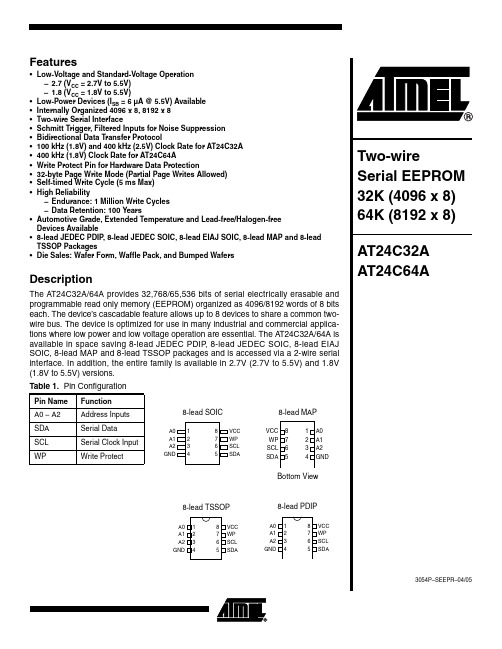
1Features•Low-Voltage and Standard-Voltage Operation –2.7 (V CC = 2.7V to 5.5V)–1.8 (V CC = 1.8V to 5.5V)•Low-Power Devices (I SB = 6 µA @ 5.5V) Available •Internally Organized 4096 x 8, 8192 x 8•Two-wire Serial Interface•Schmitt Trigger, Filtered Inputs for Noise Suppression •Bidirectional Data Transfer Protocol•100 kHz (1.8V) and 400 kHz (2.5V) Clock Rate for AT24C32A •400 kHz (1.8V) Clock Rate for AT24C64A•Write Protect Pin for Hardware Data Protection•32-byte Page Write Mode (Partial Page Writes Allowed)•Self-timed Write Cycle (5 ms Max)•High Reliability–Endurance: 1 Million Write Cycles–Data Retention: 100 Years•Automotive Grade, Extended Temperature and Lead-free/Halogen-free Devices Available•8-lead JEDEC PDIP , 8-lead JEDEC SOIC, 8-lead EIAJ SOIC, 8-lead MAP and 8-lead TSSOP Packages•Die Sales: Wafer Form, Waffle Pack, and Bumped WafersDescriptionThe AT24C32A/64A provides 32,768/65,536 bits of serial electrically erasable and programmable read only memory (EEPROM) organized as 4096/8192 words of 8 bits each. The device’s cascadable feature allows up to 8 devices to share a common two-wire bus. The device is optimized for use in many industrial and commercial applica-tions where low power and low voltage operation are essential. The AT24C32A/64A is available in space saving 8-lead JEDEC PDIP , 8-lead JEDEC SOIC, 8-lead EIAJ SOIC, 8-lead MAP and 8-lead TSSOP packages and is accessed via a 2-wire serial interface. In addition, the entire family is available in 2.7V (2.7V to 5.5V) and 1.8V (1.8V to 5.5V) versions.Table 1. Pin ConfigurationPin Name Function A0 – A2Address Inputs SDA Serial Data SCL Serial Clock Input WPWrite Protect8-lead PDIP8-lead SOIC8-lead TSSOP8-lead MAPBottom View2AT24C32A/64A3054P–SEEPR–04/05Figure 1. Block DiagramAbsolute Maximum Ratings*Operating T emperature..................................–55°C to +125°C *NOTICE:Stresses beyond those listed under “Absolute Maximum Ratings” may cause permanent dam-age to the device. This is a stress rating only and functional operation of the device at these or any other conditions beyond those indicated in the operational sections of this specification is not implied. Exposure to absolute maximum rating conditions for extended periods may affect device reliability.Storage T emperature.....................................–65°C to +150°C Voltage on Any Pinwith Respect to Ground....................................–1.0V to +7.0V Maximum Operating Voltage ..........................................6.25V DC Output Current........................................................5.0 mA3AT24C32A/64A3054P–SEEPR–04/05Pin DescriptionSERIAL CLOCK (SCL): The SCL input is used to positive edge clock data into each EEPROM device and negative edge clock data out of each device.SERIAL DATA (SDA): The SDA pin is bidirectional for serial data transfer. This pin is open-drain driven and may be wire-ORed with any number of other open-drain or open collector devices.DEVICE/ADDRESSES (A2, A1, A0): The A2, A1 and A0 pins are device address inputs that are hardwired or left not connected for hardware compatibility with other AT24Cxx devices. When the pins are hardwired, as many as eight 32K/64K devices may be addressed on a single bus system (device addressing is discussed in detail under the Device Addressing section). If the pins are left floating, the A2, A1 and A0 pins will be internally pulled down to GND if the capacitive coupling to the circuit board V CC plane is <3 pF. If coupling is >3 pF, Atmel recommends connecting the address pins to GND.WRITE PROTECT (WP): The write protect input, when connected to GND, allows nor-mal write operations. When WP is connected high to V CC , all write operations to the memory are inhibited. If the pin is left floating, the WP pin will be internally pulled down to GND if the capacitive coupling to the circuit board V CC plane is <3 pF. If coupling is >3pF, Atmel recommends connecting the pin to GND. Switching WP to V CC prior to a write operation creates a software write protect function.Memory OrganizationAT24C32A/64A, 32K/64K SERIAL EEPROM: The 32K/64K is internally organized as 128/256 pages of 32 bytes each. Random word addressing requires a 12/13-bit data word address.4AT24C32A/64A3054P–SEEPR–04/05Note:1.This parameter is characterized and is not 100% tested.Note:1.V IL min and V IH max are reference only and are not tested.Table 2. Pin Capacitance (1)Applicable over recommended operating range from T A = 25°C, f = 1.0 MHz, V CC = +1.8V.Symbol Test ConditionMax Units Conditions C I/O Input/Output Capacitance (SDA)8pF V I/O = 0V C IN Input Capacitance (A 0, A 1, A 2, SCL)6pFV IN = 0VTable 3. DC CharacteristicsApplicable over recommended operating range from: T AI = –40°C to +85°C, V CC = +1.8V to +5.5V, T AE = –40°C to +125°C,V CC = +1.8V to +5.5V (unless otherwise noted).Symbol Parameter Test ConditionMin TypMax Units V CC1Supply Voltage 1.8 5.5V V CC2Supply Voltage 2.5 5.5V V CC3Supply Voltage 2.7 5.5V V CC4Supply Voltage 4.55.5V I CC1Supply Current V CC = 5.0V READ at 400 kHz 0.4 1.0mA I CC2Supply Current V CC = 5.0V WRITE at 400 kHz 2.0 3.0mA I SB1Standby Current (1.8V option)V CC = 1.8V V IN = V CC or V SS 1.0µA I SB2Standby Current (2.5V option)V CC = 2.5V V IN = V CC or V SS 2.0µA I SB3Standby Current (2.7V option)V CC = 2.7V V IN = V CC or V SS 2.0µA I SB4Standby Current (5V option)V CC = 4.5 - 5.5V V IN = V CC or V SS6.0µA I LI Input Leakage CurrentV IN = V CC or V SS 0.10 3.0µA I LO Output Leakage Current V OUT = V CC or V SS0.053.0µA V IL (1)Input Low Level –0.6V CC x 0.3V V IH (1)Input High Level V CC x 0.7V CC + 0.5V V OL2Output Low Level V CC = 3.0V I OL = 2.1 mA 0.4V V OL1Output Low LevelV CC = 1.8VI OL = 0.15 mA0.2V5AT24C32A/64A3054P–SEEPR–04/05Notes:1.This parameter is characterized and is not 100% tested.2.This parameter is characterized and is not 100% tested (T A = 25°C).3.The Write Cycle Time of 5 ms only applies to the A T24C32A/64A devices bearing the process letter “A” on the package (themark is located in the lower right corner on the top side of the package).Table 4. AC CharacteristicsApplicable over recommended operating range from T AI = –40°C to +85°C, T AE = –40°C to +125°C, V CC = +1.8V to +5.5V,CL = 1 TTL Gate and100 pF (unless otherwise noted).Symbol ParameterAT24C32A AT24C64AUnits 1.8V2.5V – 5.0V 1.8V –3.6V 5.0VMinMax MinMax MinMax MinMax f SCL Clock Frequency, SCL 100400400400kHz t LOW Clock Pulse Width Low 4.7 1.3 1.3 1.2µs t HIGH Clock Pulse Width High 4.00.60.60.6µs t I Noise Suppression Time (1)1005010050ns t AA Clock Low to Data Out Valid 0.1 4.50.10.90.20.90.10.9µs t BUF Time the bus must be free before a new transmission can start (1) 4.7 1.3 1.3 1.2µs t HD.ST A Start Hold Time 4.00.60.60.6µs t SU.ST A Start Set-up Time 4.70.60.60.6µs t HD.DA T Data In Hold Time 0000µs t SU.DAT Data In Set-up Time 200100100100ns t R (1)Inputs Rise Time 1.00.30.30.3µs t F (1)Inputs Fall Time 300300300300ns t SU.STO Stop Set-up Time 4.70.60.60.6µs t DH Data Out Hold Time 1005020050ns t WRWrite Cycle Time 20 or 5(3)10 or 5(3)20 or 5(3)10 or 5(3)ms Endurance (1) 5.0V , 25°C, Page Mode1M 1M1M1MWrite Cycles6AT24C32A/64A3054P–SEEPR–04/05Device OperationCLOCK and DATA TRANSITIONS: The SDA pin is normally pulled high with an exter-nal device. Data on the SDA pin may change only during SCL low time periods (refer to Data Validity timing diagram). Data changes during SCL high periods will indicate a start or stop condition as defined below.START CONDITION: A high-to-low transition of SDA with SCL high is a start condition which must precede any other command (see Figure 5 on page 8).STOP CONDITION: A low-to-high transition of SDA with SCL high is a stop condition.After a read sequence, the stop command will place the EEPROM in a standby power mode (see Figure 5 on page 8).ACKNOWLEDGE: All addresses and data words are serially transmitted to and from the EEPROM in 8-bit words. The EEPROM sends a zero during the ninth clock cycle to acknowledge that it has received each word.STANDBY MODE: The AT24C32A/64A features a low power standby mode which is enabled: a) upon power-up and b) after the receipt of the stop bit and the completion of any internal operations.MEMORY RESET: After an interruption in protocol, power loss or system reset, any two-wire part can be reset by following these steps:(a) Clock up to 9 cycles, (b) look for SDA high in each cycle while SCL is high and then (c) create a start condition as SDA is high.7AT24C32A/64A3054P–SEEPR–04/05Figure 2. Bus TimingSCL: Serial Clock, SDA: Serial Data I/OFigure 3. Write Cycle TimingSCL: Serial Clock, SDA: Serial Data I/ONote:1.The write cycle time t WR is the time from a valid stop condition of a write sequence to the end of the internal clear/write cycle.Figure 4.Data Validity8AT24C32A/64A3054P–SEEPR–04/05Figure 5. Start and Stop DefinitionFigure 6.Output Acknowledge9AT24C32A/64A3054P–SEEPR–04/05Device AddressingThe 32K/64K EEPROM requires an 8-bit device address word following a start condition to enable the chip for a read or write operation (see Figure 7 on page 11). The device address word consists of a mandatory one, zero sequence for the first four most signifi-cant bits as shown. This is common to all 2-wire EEPROM devices.The 32K/64K uses the three device address bits A2, A1, A0 to allow as many as eight devices on the same bus. These bits must compare to their corresponding hardwired input pins. The A2, A1, and A0 pins use an internal proprietary circuit that biases them to a logic low condition if the pins are allowed to float.The eighth bit of the device address is the read/write operation select bit. A read opera-tion is initiated if this bit is high and a write operation is initiated if this bit is low.Upon a compare of the device address, the EEPROM will output a zero. If a compare is not made, the device will return to standby state.NOISE PROTECTION: Special internal circuitry placed on the SDA and SCL pins pre-vent small noise spikes from activating the device.DATA SECURITY: The AT24C32A/64A has a hardware data protection scheme that allows the user to write protect the entire memory when the WP pin is at V CC .Write OperationsBYTE WRITE: A write operation requires two 8-bit data word addresses following the device address word and acknowledgment. Upon receipt of this address, the EEPROM will again respond with a zero and then clock in the first 8-bit data word. Following receipt of the 8-bit data word, the EEPROM will output a zero and the addressing device, such as a microcontroller, must terminate the write sequence with a stop condi-tion. At this time the EEPROM enters an internally-timed write cycle, t WR , to the nonvolatile memory. All inputs are disabled during this write cycle and the EEPROM will not respond until the write is complete (see Figure 8 on page 11).PAGE WRITE: The 32K/64K EEPROM is capable of 32-byte page writes.A page write is initiated the same way as a byte write, but the microcontroller does not send a stop condition after the first data word is clocked in. Instead, after the EEPROM acknowledges receipt of the first data word, the microcontroller can transmit up to 31more data words. The EEPROM will respond with a zero after each data word received.The microcontroller must terminate the page write sequence with a stop condition (see Figure 9 on page 11).The data word address lower five bits are internally incremented following the receipt of each data word. The higher data word address bits are not incremented, retaining the memory page row location. When the word address, internally generated, reaches the page boundary, the following byte is placed at the beginning of the same page. If more than 32 data words are transmitted to the EEPROM, the data word address will “roll over” and previous data will be overwritten.ACKNOWLEDGE POLLING: Once the internally-timed write cycle has started and the EEPROM inputs are disabled, acknowledge polling can be initiated. This involves send-ing a start condition followed by the device address word. The read/write bit is representative of the operation desired. Only if the internal write cycle has completed will the EEPROM respond with a zero, allowing the read or write sequence to continue.10AT24C32A/64A3054P–SEEPR–04/05Read OperationsRead operations are initiated the same way as write operations with the exception that the read/write select bit in the device address word is set to one. There are three read operations: current address read, random address read and sequential read.CURRENT ADDRESS READ: The internal data word address counter maintains the last address accessed during the last read or write operation, incremented by one. This address stays valid between operations as long as the chip power is maintained. The address “roll over” during read is from the last byte of the last memory page, to the first byte of the first page. The address “roll over” during write is from the last byte of the cur-rent page to the first byte of the same page.Once the device address with the read/write select bit set to one is clocked in and acknowledged by the EEPROM, the current address data word is serially clocked out.The microcontroller does not respond with an input zero but does generate a following stop condition (see Figure 10 on page 11).RANDOM READ: A random read requires a “dummy” byte write sequence to load in the data word address. Once the device address word and data word address are clocked in and acknowledged by the EEPROM, the microcontroller must generate another start condition. The microcontroller now initiates a current address read by sending a device address with the read/write select bit high. The EEPROM acknowledges the device address and serially clocks out the data word. The microcontroller does not respond with a zero but does generate a following stop condition (see Figure 11 on page 12).SEQUENTIAL READ: Sequential reads are initiated by either a current address read or a random address read. After the microcontroller receives a data word, it responds with an acknowledge. As long as the EEPROM receives an acknowledge, it will continue to increment the data word address and serially clock out sequential data words. When the memory address limit is reached, the data word address will “roll over” and the sequen-tial read will continue. The sequential read operation is terminated when the microcontroller does not respond with a zero but does generate a following stop condi-tion (see Figure 12 on page 12).11AT24C32A/64A3054P–SEEPR–04/05Figure 7. Device AddressFigure 8. Byte WriteFigure 9. Page WriteNotes:1.* = DON’T CARE bits2.† = DON’T CARE bits for the 32KFigure 10.Current Address Read12AT24C32A/64A3054P–SEEPR–04/05Figure 11. Random ReadNote: 1.* = DON’T CARE bitsFigure 12.Sequential Read13AT24C32A/64A3054P–SEEPR–04/05Notes:1.For2.7V devices used in the 4.5V to 5.5V range, please refer to performance values in the AC and DC Characteristicstables.2.“U” and “Q” designate Green package and ROHS Compliance.3.Available in waffle pack and wafer form; order as SL719 for wafer form. Bumped die available upon request. Please contactSerial EEPROM Marketing.AT24C32A Ordering Information (1)Ordering Code Package Operation Range A T24C32A-10PI-2.7A T24C32AN-10SI-2.7A T24C32AW-10SI-2.7A T24C32A-10TI-2.78P38S18S28A2Industrial Temperature (–40°C to 85°C)A T24C32A-10PI-1.8A T24C32AN-10SI-1.8A T24C32AW-10SI-1.8A T24C32A-10TI-1.88P38S18S28A2Industrial Temperature (–40°C to 85°C)A T24C32A-10PU-2.7(2)A T24C32A-10PU-1.8(2)A T24C32AN-10SU-2.7(2)A T24C32AN-10SU-1.8(2)A T24C32AW-10SU-2.7(2)A T24C32AW-10SU-1.8(2)A T24C32A-10TU-2.7(2)A T24C32A-10TU-1.8(2)A T24C32AY1-10YU-1.8(2)8P38P38S18S18S28S28A28A28Y1Lead-free/Halogen-free/Industrial Temperature (–40°C to 85°C)A T24C32A-10PQ-2.7(2)A T24C32AN-10SQ-2.7(2)A T24C32A-10TQ-2.7(2)8P38S18A2Lead-free/Halogen-free/Extended T emperature (–40°C to 125°C)A T24C32A-10PE-2.7A T24C32AN-10SE-2.78P38S1Extended T emperature (–40°C to 125°C)A T24C32A-W2.7-11(3)A T24C32A-W1.8-11(3)Die Sale Die SaleIndustrial Temperature (–40°C to 85°C)Package Type8P38-lead, 0.300" Wide, Plastic Dual In-line Package (PDIP)8S18-lead, 0.150" Wide, Plastic Gull Wing Small Outline (JEDEC SOIC)8S28-lead, 0.209" Body, Plastic Small Outline (EIAJ SOIC)8A28-lead, 4.4 mm Body, Plastic Thin Shrink Small Outline Package (TSSOP)8Y18-lead, 4.90 mm x 3.00 mm Body, Dual Footprint, Non-leaded, Miniature Array Package (MAP)Options–2.7Low Voltage (2.7V to 5.5V)–1.8Low Voltage (1.8V to 5.5V)14AT24C32A/64A3054P–SEEPR–04/05Notes:1.For2.7V devices used in the 4.5V to 5.5V range, please refer to performance values in the AC and DC Characteristicstables.2.“U” and “Q” designate Green package and ROHS Compliance.3.Available in waffle pack and wafer form; order as SL719 for wafer form. Bumped die available upon request. Please contactSerial EEPROM Marketing.AT24C64A Ordering Information (1)Ordering Code Package Operation Range A T24C64A-10PI-2.7A T24C64AN-10SI-2.7A T24C64AW-10SI-2.7A T24C64A-10TI-2.78P38S18S28A2Industrial Temperature (–40°C to 85°C)A T24C64A-10PI-1.8A T24C64AN-10SI-1.8A T24C64AW-10SI-1.8A T24C64A-10TI-1.88P38S18S28A2Industrial Temperature (–40°C to 85°C)A T24C64A-10PU-2.7(2)A T24C64A-10PU-1.8(2)A T24C64AN-10SU-2.7(2)A T24C64AN-10SU-1.8(2)A T24C64AW-10SU-2.7(2)A T24C64AW-10SU-1.8(2)A T24C64A-10TU-2.7(2)A T24C64A-10TU-1.8(2)A T24C64AY1-10YU-1.8(2)8P38P38S18S18S28S28A28A28Y1Lead-free/Halogen-free/Industrial Temperature (–40°C to 85°C)A T24C64A-10PQ-2.7(2)A T24C64AN-10SQ-2.7(2)A T24C64A-10TQ-2.7(2)8P38S18A2Lead-free/Halogen-free/Extended T emperature (–40°C to 125°C)A T24C64A-10PE-2.7A T24C64AN-10SE-2.78P38S1Extended T emperature (–40°C to 125°C)A T24C64A-W2.7-11(3)A T24C64A-W1.8-11(3)Die Sale Die SaleIndustrial Temperature (–40°C to 85°C)Package Type8P38-lead, 0.300" Wide, Plastic Dual In-line Package (PDIP)8S18-lead, 0.150" Wide, Plastic Gull Wing Small Outline (JEDEC SOIC)8S28-lead, 0.209" Body, Plastic Small Outline (EIAJ SOIC)8A28-lead, 4.4mm Body, Plastic Thin Shrink Small Outline Package (TSSOP)8Y18-lead, 4.90 mm x 3.00 mm Body, Dual Footprint, Non-leaded, Miniature Array Package (MAP)Options–2.7Low Voltage (2.7V to 5.5V)–1.8Low Voltage (1.8V to 5.5V)15AT24C32A/64A3054P–SEEPR–04/05Package Drawings8P3 – PDIP16AT24C32A/64A3054P–SEEPR–04/058S1 – JEDEC SOIC17AT24C32A/64A3054P–SEEPR–04/058S2 – EIAJ SOIC18AT24C32A/64A3054P–SEEPR–04/058A2 – TSSOP19AT24C32A/64A3054P–SEEPR–04/058Y1 – MAP3054P–SEEPR–04/05Disclaimer: The information in this document is provided in connection with Atmel products. No license, express or implied, by estoppel or otherwise,to any intellectual property right is granted by this document or in connection with the sale of Atmel products. EXCEPT AS SET FORTH IN ATMEL ’S TERMS AND CONDI-TIONS OF SALE LOCATED ON ATMEL ’S WEB SITE, ATMEL ASSUMES NO LIABILITY WHATSOEVER AND DISCLAIMS ANY EXPRESS, IMPLIED OR STATUTORY WARRANTY RELATING TO ITS PRODUCTS INCLUDING, BUT NOT LIMITED TO, THE IMPLIED WARRANTY OF MERCHANTABILITY, FITNESS FOR A PARTICULAR PURPOSE, OR NON-INFRINGEMENT. IN NO EVENT SHALL ATMEL BE LIABLE FOR ANY DIRECT, INDIRECT, CONSEQUENTIAL, PUNITIVE, SPECIAL OR INCIDEN-TAL DAMAGES (INCLUDING, WITHOUT LIMITATION, DAMAGES FOR LOSS OF PROFITS, BUSINESS INTERRUPTION, OR LOSS OF INFORMATION) ARISING OUT OF THE USE OR INABILITY TO USE THIS DOCUMENT, EVEN IF ATMEL HAS BEEN ADVISED OF THE POSSIBILITY OF SUCH DAMAGES. Atmel makes no representations or warranties with respect to the accuracy or completeness of the contents of this document and reserves the right to make changes to specifications and product descriptions at any time without notice. Atmel does not make any commitment to update the information contained herein. Atmel’s products are not intended, authorized, or warranted for use as components in applications intended to support or sustain life.Atmel CorporationAtmel Operations2325 Orchard Parkway San Jose, CA 95131, USA Tel: 1(408) 441-0311Fax: 1(408) 487-2600Regional HeadquartersEuropeAtmel SarlRoute des Arsenaux 41Case Postale 80CH-1705 Fribourg SwitzerlandTel: (41) 26-426-5555Fax: (41) 26-426-5500AsiaRoom 1219Chinachem Golden Plaza 77 Mody Road Tsimshatsui East Kowloon Hong KongTel: (852) 2721-9778Fax: (852) 2722-1369Japan9F, Tonetsu Shinkawa Bldg.1-24-8 ShinkawaChuo-ku, Tokyo 104-0033JapanTel: (81) 3-3523-3551Fax: (81) 3-3523-7581Memory2325 Orchard Parkway San Jose, CA 95131, USA Tel: 1(408) 441-0311Fax: 1(408) 436-4314Microcontrollers2325 Orchard Parkway San Jose, CA 95131, USA Tel: 1(408) 441-0311Fax: 1(408) 436-4314La Chantrerie BP 7060244306 Nantes Cedex 3, France Tel: (33) 2-40-18-18-18Fax: (33) 2-40-18-19-60ASIC/ASSP/Smart CardsZone Industrielle13106 Rousset Cedex, France Tel: (33) 4-42-53-60-00Fax: (33) 4-42-53-60-011150 East Cheyenne Mtn. Blvd.Colorado Springs, CO 80906, USA Tel: 1(719) 576-3300Fax: 1(719) 540-1759Scottish Enterprise Technology Park Maxwell BuildingEast Kilbride G75 0QR, Scotland Tel: (44) 1355-803-000Fax: (44) 1355-242-743RF/AutomotiveTheresienstrasse 2Postfach 353574025 Heilbronn, Germany Tel: (49) 71-31-67-0Fax: (49) 71-31-67-23401150 East Cheyenne Mtn. Blvd.Colorado Springs, CO 80906, USA Tel: 1(719) 576-3300Fax: 1(719) 540-1759Biometrics/Imaging/Hi-Rel MPU/High Speed Converters/RF DatacomAvenue de Rochepleine BP 12338521 Saint-Egreve Cedex, France Tel: (33) 4-76-58-30-00Fax: (33) 4-76-58-34-80Literature Requests/literature© Atmel Corporation 2005. All rights reserved. Atmel ®, logo and combinations thereof, Everywhere You Are ® and others are registered trade-marks, and others are the trademarks of Atmel Corporation or its subsidiaries. Other terms and product names may be trademarks of others.。

Features•Standard-Voltage Operation –2.7 (V CC = 2.7V to 5.5V)•Internally Organized 4096 x 8 (32K), 8192 x 8 (64K)•Automotive Temperature Range –40°C to +125°C •Two-wire Serial Interface•Schmitt Trigger, Filtered Inputs for Noise Suppression •Bidirectional Data Transfer Protocol •400 kHz Clock Rate•Write Protect Pin for Hardware Data Protection•32-byte Page Write Mode (Partial Page Writes Allowed)•Self-timed Write Cycle (5 ms Max)•High Reliability–Endurance: 1 Million Write Cycles –Data Retention: 100 Years•Lead-free/Halogen-free Devices Available•8-lead JEDEC SOIC and 8-lead TSSOP PackagesDescriptionThe AT24C32A/64A provides 32,768/65,536 bits of serial electrically erasable and programmable read only memory (EEPROM) organized as 4096/8192 words of 8 bits each. The device’s cascadable feature allows up to 8 devices to share a common two-wire bus. The device is optimized for use in many automotive applications where low power and low voltage operation are essential. The AT24C32A/64A is available in space saving 8-lead JEDEC SOIC and 8-lead TSSOP packages and is accessed via a 2-wire serial interface and is available in a 2.7V (2.7V to 5.5V) version.Table 1. Pin ConfigurationPin Name Function A0 – A2Address InputsSDA Serial Data SCL Serial Clock Input WPWrite Protect8-lead SOIC8-lead TSSOPBDTIC www.BDTIC .com/ATMEL25120D–SEEPR–6/08AT24C32A/64AFigure 1. Block DiagramAbsolute Maximum Ratings*Operating T emperature..................................–55°C to +125°C *NOTICE:Stresses beyond those listed under “Absolute Maximum Ratings” may cause permanent dam-age to the device. This is a stress rating only and functional operation of the device at these or any other conditions beyond those indicated in the operational sections of this specification is not implied. Exposure to absolute maximum rating conditions for extended periods may affect device reliability.Storage T emperature.....................................–65°C to +150°C Voltage on Any Pinwith Respect to Ground....................................–1.0V to +7.0V Maximum Operating Voltage ..........................................6.25V DC Output Current........................................................5.0 mA35120D–SEEPR–6/08AT24C32A/64APin DescriptionSERIAL CLOCK (SCL): The SCL input is used to positive edge clock data into each EEPROM device and negative edge clock data out of each device.SERIAL DATA (SDA): The SDA pin is bidirectional for serial data transfer. This pin is open-drain driven and may be wire-ORed with any number of other open-drain or open collector devices.DEVICE/ADDRESSES (A2, A1, A0): The A2, A1 and A0 pins are device address inputs that are hardwired or left not connected for hardware compatibility with other AT24Cxx devices. When the pins are hardwired, as many as eight 32K/64K devices may be addressed on a single bus system (device addressing is discussed in detail under the Device Addressing section). If the pins are left floating, the A2, A1 and A0 pins will be internally pulled down to GND if the capaci-tive coupling to the circuit board V CC plane is <3 pF. If coupling is >3 pF, Atmel recommends connecting the address pins to GND.WRITE PROTECT (WP): The write protect input, when connected to GND, allows normal write operations. When WP is connected high to V CC , all write operations to the memory are inhibited.If the pin is left floating, the WP pin will be internally pulled down to GND if the capacitive cou-pling to the circuit board V CC plane is <3 pF. If coupling is >3pF, Atmel recommends connecting the pin to GND. Switching WP to V CC prior to a write operation creates a software write protect function.Memory OrganizationAT24C32A/64A, 32K/64K SERIAL EEPROM: The 32K/64K is internally organized as 128/256pages of 32 bytes each. Random word addressing requires a 12/13-bit data word address.45120D–SEEPR–6/08AT24C32A/64ANote:1.This parameter is characterized and is not 100% tested.IL IH Table 2. Pin Capacitance (1)Applicable over recommended operating range from T A = 25°C, f = 1.0 MHz, V CC = +2.7V to +5.5VSymbol Test ConditionMax Units Conditions C I/O Input/Output Capacitance (SDA)8pF V I/O = 0V C IN Input Capacitance (A 0, A 1, A 2, SCL)6pFV IN = 0VTable 3. DC CharacteristicsApplicable over recommended operating range from: T A = –40°C to +125°C,V CC = +2.7V to +5.5V (unless otherwise noted)Symbol Parameter Test ConditionMin TypMax Units V CC3Supply Voltage 2.75.5V I CC1Supply Current V CC = 5.0V READ at 400 kHz 0.4 1.0mA I CC2Supply Current V CC = 5.0V WRITE at 400 kHz 2.0 3.0mA I SB Standby Current V CC = 2.7V V IN = V CC or V SS1.0 3.0µA V CC = 5.0V 3.0 5.0I LI Input Leakage CurrentV IN = V CC or V SS 0.10 3.0µA I LO Output Leakage Current V OUT = V CC or V SS0.05 3.0µA V IL (1)Input Low Level –0.6V CC x 0.3V V IH (1)Input High Level V CC x 0.7V CC + 0.5V V OL2Output Low LevelV CC = 3.0VI OL = 2.1 mA0.4V V OL1Output Low Level V CC = 1.8V I OL = 0.15 mA 0.2V55120D–SEEPR–6/08AT24C32A/64ANotes: 1.This parameter is ensured by characterization only.Table 4. AC CharacteristicsApplicable over recommended operating range from T A = –40°C to +125°C, V CC = +2.7V to +5.5V, CL = 1 TTL Gate and 100 pF (unless otherwise noted)Symbol ParameterAT24C32A/AT24C64AUnits 2.7V – 5.5VMinMax f SCL Clock Frequency, SCL 400kHz t LOW Clock Pulse Width Low 1.2µs t HIGH Clock Pulse Width High 0.6µs t I Noise Suppression Time (1)50ns t AA Clock Low to Data Out Valid 0.10.9µs t BUF Time the bus must be free before a new transmission can start (1) 1.2µs t HD.ST A Start Hold Time 0.6µs t SU.ST A Start Set-up Time 0.6µs t HD.DA T Data In Hold Time 0µs t SU.DAT Data In Set-up Time 100ns t R (1)Inputs Rise Time 0.3µs t F (1)Inputs Fall Time 300ns t SU.STO Stop Set-up Time 0.6µs t DH Data Out Hold Time 50ns t WRWrite Cycle Time5ms Endurance (1) 5.0V , 25⋅C, Page Mode1M Write Cycles65120D–SEEPR–6/08AT24C32A/64ADevice OperationCLOCK and DATA TRANSITIONS: The SDA pin is normally pulled high with an external device. Data on the SDA pin may change only during SCL low time periods (refer to Data Valid-ity timing diagram). Data changes during SCL high periods will indicate a start or stop condition as defined below.START CONDITION: A high-to-low transition of SDA with SCL high is a start condition which must precede any other command (see Figure 5 on page 8).STOP CONDITION: A low-to-high transition of SDA with SCL high is a stop condition. After a read sequence, the stop command will place the EEPROM in a standby power mode (see Fig-ure 5 on page 8).ACKNOWLEDGE: All addresses and data words are serially transmitted to and from the EEPROM in 8-bit words. The EEPROM sends a zero during the ninth clock cycle to acknowl-edge that it has received each word.STANDBY MODE: The AT24C32A/64A features a low power standby mode which is enabled:a) upon power-up and b) after the receipt of the stop bit and the completion of any internal operations.MEMORY RESET: After an interruption in protocol, power loss or system reset, any two-wire part can be reset by following these steps:(a) Clock up to 9 cycles, (b) look for SDA high in each cycle while SCL is high and then (c) create a start condition as SDA is high.75120D–SEEPR–6/08AT24C32A/64AFigure 2. Bus TimingSCL: Serial Clock, SDA: Serial Data I/OFigure 3. Write Cycle TimingSCL: Serial Clock, SDA: Serial Data I/ONote:1.The write cycle time t WR is the time from a valid stop condition of a write sequence to the end of the internal clear/write cycle.Figure 4.Data Validity85120D–SEEPR–6/08AT24C32A/64AFigure 5. Start and Stop DefinitionFigure 6.Output Acknowledge95120D–SEEPR–6/08AT24C32A/64ADeviceAddressingThe 32K/64K EEPROM requires an 8-bit device address word following a start condition to enable the chip for a read or write operation (see Figure 7 on page 11). The device address word consists of a mandatory one, zero sequence for the first four most significant bits as shown. This is common to all 2-wire EEPROM devices.The 32K/64K uses the three device address bits A2, A1, A0 to allow as many as eight devices on the same bus. These bits must compare to their corresponding hardwired input pins. The A2,A1, and A0 pins use an internal proprietary circuit that biases them to a logic low condition if the pins are allowed to float.The eighth bit of the device address is the read/write operation select bit. A read operation is ini-tiated if this bit is high and a write operation is initiated if this bit is low.Upon a compare of the device address, the EEPROM will output a zero. If a compare is not made, the device will return to standby state.NOISE PROTECTION: Special internal circuitry placed on the SDA and SCL pins prevent small noise spikes from activating the device.DATA SECURITY: The AT24C32A/64A has a hardware data protection scheme that allows the user to write protect the entire memory when the WP pin is at V CC .WriteOperationsBYTE WRITE: A write operation requires two 8-bit data word addresses following the device address word and acknowledgment. Upon receipt of this address, the EEPROM will again respond with a zero and then clock in the first 8-bit data word. Following receipt of the 8-bit data word, the EEPROM will output a zero and the addressing device, such as a microcontroller,must terminate the write sequence with a stop condition. At this time the EEPROM enters an internally-timed write cycle, t WR , to the nonvolatile memory. All inputs are disabled during this write cycle and the EEPROM will not respond until the write is complete (see Figure 8 on page 11).PAGE WRITE: The 32K/64K EEPROM is capable of 32-byte page writes.A page write is initiated the same way as a byte write, but the microcontroller does not send a stop condition after the first data word is clocked in. Instead, after the EEPROM acknowledges receipt of the first data word, the microcontroller can transmit up to 31 more data words. The EEPROM will respond with a zero after each data word received. The microcontroller must ter-minate the page write sequence with a stop condition (see Figure 9 on page 11).The data word address lower five bits are internally incremented following the receipt of each data word. The higher data word address bits are not incremented, retaining the memory page row location. When the word address, internally generated, reaches the page boundary, the fol-lowing byte is placed at the beginning of the same page. If more than 32 data words are transmitted to the EEPROM, the data word address will “roll over” and previous data will be overwritten.ACKNOWLEDGE POLLING: Once the internally-timed write cycle has started and the EEPROM inputs are disabled, acknowledge polling can be initiated. This involves sending a start condition followed by the device address word. The read/write bit is representative of the operation desired. Only if the internal write cycle has completed will the EEPROM respond with a zero, allowing the read or write sequence to continue.105120D–SEEPR–6/08AT24C32A/64AReadOperationsRead operations are initiated the same way as write operations with the exception that the read/write select bit in the device address word is set to one. There are three read operations:current address read, random address read and sequential read.CURRENT ADDRESS READ: The internal data word address counter maintains the last address accessed during the last read or write operation, incremented by one. This address stays valid between operations as long as the chip power is maintained. The address “roll over”during read is from the last byte of the last memory page, to the first byte of the first page. The address “roll over” during write is from the last byte of the current page to the first byte of the same page.Once the device address with the read/write select bit set to one is clocked in and acknowledged by the EEPROM, the current address data word is serially clocked out. The microcontroller does not respond with an input zero but does generate a following stop condition (see Figure 10 on page 11).RANDOM READ: A random read requires a “dummy” byte write sequence to load in the data word address. Once the device address word and data word address are clocked in and acknowledged by the EEPROM, the microcontroller must generate another start condition. The microcontroller now initiates a current address read by sending a device address with the read/write select bit high. The EEPROM acknowledges the device address and serially clocks out the data word. The microcontroller does not respond with a zero but does generate a follow-ing stop condition (see Figure 11 on page 12).SEQUENTIAL READ: Sequential reads are initiated by either a current address read or a ran-dom address read. After the microcontroller receives a data word, it responds with an acknowledge. As long as the EEPROM receives an acknowledge, it will continue to increment the data word address and serially clock out sequential data words. When the memory address limit is reached, the data word address will “roll over” and the sequential read will continue. The sequential read operation is terminated when the microcontroller does not respond with a zero but does generate a following stop condition (see Figure 12 on page 12).115120D–SEEPR–6/08AT24C32A/64AFigure 7. Device AddressFigure 8. Byte WriteFigure 9. Page WriteNotes:1.* = DON’T CARE bits2.† = DON’T CARE bits for the 32KFigure 10.Current Address Read125120D–SEEPR–6/08AT24C32A/64AFigure 11. Random ReadNote: 1.* = DON’T CARE bitsFigure 12.Sequential Read135120D–SEEPR–6/08AT24C32A/64ANotes:1.For2.7V devices used in the 4.5V to 5.5V range, please refer to performance values in the AC and DC Characteristicstables.2.“Q” designates Green package and RoHS Compliant.AT24C32A Ordering Information (1)Ordering Code Package Operation Range A T24C32AN-10SQ-2.7(2)A T24C32A-10TQ-2.7(2)8S18A2Lead-free/Halogen-free/Automotive (–40⋅C to 125⋅C)Package Type8S18-lead, 0.150" Wide, Plastic Gull Wing Small Outline (JEDEC SOIC)8A28-lead, 4.4 mm Body, Plastic Thin Shrink Small Outline Package (TSSOP)Options–2.7Low Voltage (2.7V to 5.5V)145120D–SEEPR–6/08AT24C32A/64ANotes:1.For2.7V devices used in the 4.5V to 5.5V range, please refer to performance values in the AC and DC Characteristicstables.2.“Q” designates Green package and RoHS Compliant.AT24C64A Ordering Information (1)Ordering Code Package Operation Range A T24C64AN-10SQ-2.7(2)A T24C64A-10TQ-2.7(2)8S18A2Lead-free/Halogen-free/Automotive (–40⋅C to 125⋅C)Package Type8S18-lead, 0.150" Wide, Plastic Gull Wing Small Outline (JEDEC SOIC)8A28-lead, 4.4mm Body, Plastic Thin Shrink Small Outline Package (TSSOP)Options–2.7Low Voltage (2.7V to 5.5V)155120D–SEEPR–6/08AT24C32A/64APackage Drawings8S1 – JEDEC SOIC165120D–SEEPR–6/08AT24C32A/64A8A2 – TSSOP175120D–SEEPR–6/08AT24C32A/64ARevision HistoryRevision HistoryRevision Date Comments5120D6/2008Implemented revision history.。

金鹏科技有限公司Golden Palm Science Technology Co.,Ltd目录一、OCM4X8C液晶显示模块概述 (1)二、模块引脚说明 (1)1)表—1:OCM2X8C(128X32)、OCM2X10C(160X32)模块引脚说明 (1)2)表—2:OCM2X8C-2(128X32)模块引脚说明 (1)3)表—3:OCM4X8C(128X64)引脚说明 (1)4)表—4:OCM4X16A(256X64)引脚说明 (2)三、OCM4X8C液晶硬件接口 (2)1、8位并行连接时序图 (2)2、串行连接时序图 (3)3、AC电气特性(TA=25℃V CC=5V) (3)四、用户指令集 (4)五、显示坐标关系 (7)1、图形显示坐标 (7)2、汉字显示坐标 (8)3、字符表 (8)六、显示步骤 (9)七、显示示例程序 (9)1、发送子程序 (9)2、读子程序 (10)八、模块尺寸图 (12)附:汉字字符集三、OCM4X8C液晶硬件接口1、逻辑工作电压(VDD):4.5~5.5V2、电源地(GND):0V3、LCD驱动电压(V0):0~-10V4、工作温度(Ta):0~55℃(常温) / -20~70℃(宽温)保存温度(Tstg):-10~65℃(常温)5、电气特性见附图1 外部连接图(参考附图2)模块有并行和串行两种连接方法(时序如下):1、8位并行连接时序图MPU写资料到模块备注:六、显示步骤1、显示资料RAM(DDRAM)显示资料RAM提供64×2个位元组的空间,最多可以控制4行16字(64个字)的中文字型显示,当写入显示资料RAM时,可以分别显示CGROM、HCGROM与CGRAM 的字型;ST7920A可以显示三种字型,分别是半宽的HCGROM字型、CGRAM字型及中文CGROM字型,三种字型的选择,由在DDRAM中写入的编码选择,在0000H—0006 H的编码中将自动的结合下一个位元组,组成两个位元组的编码达成中文字型的编码(A140—D75F),各种字型详细编码如下:1、显示半宽字型:将8位元资料写入DDRAM中,范围为02H—7FH的编码。
高性能32位多核处理器SOC芯片S698PM用户手册(Ver:4.8)珠海欧比特宇航科技股份有限公司地址: 广东省珠海市唐家东岸白沙路1号欧比特科技园邮编: 519080 电话*************传真*************网址: 修改记录版权声明珠海欧比特宇航科技股份有限公司拥有此文件的版权,并有权将其作为保密资料处理。
本文件包含由版权法保护的专有资料,版权所有,未经珠海欧比特宇航科技股份有限公司的书面同意不得将本文件的任何部分进行照相、复制、公开、转载或以其他方式散发给第三方,否则,必将追究其法律责任。
免责声明本文档仅提供阶段性信息,所含内容可根据产品的实际情况随时更新,恕不另行通知。
如因文档使用不当造成的直接或间接损失,珠海欧比特宇航科技股份有限公司不承担任何责任。
珠海欧比特宇航科技股份有限公司ZHUHAI ORBITA AEROSPACE SCIENCE & TECHNOLOGY CO. , LTD地址(Addr):广东省珠海市唐家东岸白沙路1号欧比特科技园Orbita Tech Park, 1 Baisha Road, Tangjia Dong,an, Zhuhai, Guangdong, China 邮编:519080电话(Tel):+86 756-3391979传真(Fax):+86 756-3391980网址(web):目录目录 (I)表目录 (IX)图目录 (1)1.概述 (1)1.1产品简介 (1)1.2结构组成 (2)1.3主要特征 (3)1.4产品订货信息 (5)2.芯片初始化 (6)2.1上电或复位初始化过程 (6)2.2上电或复位需初始化参数配置 (8)2.3多核软件程序启动过程 (10)3.时钟信号发生模块 (10)3.1片内时钟域 (10)3.2时钟信号发生模块 (12)4.处理器核心 (15)4.1整型单元IU (15)4.1.1 主要特性 (15)4.1.2 指令 (16)4.1.3 寄存器堆(Register File) (19)4.1.4 专用寄存器 (22)4.1.5 异常(Exception) (27)4.1.6 复位操作 (29)4.1.7 休眠模式(Power-down) (29)4.1.8 多核处理器支持 (30)4.2浮点单元(FPU)和浮点控制器(FPC) (30)4.2.1 FPU概述 (30)4.2.2 FPU功能描述 (30)4.2.3 FPC概述 (35)4.2.4 FPC的浮点寄存器文件(Floating-Point register file) (35)4.2.5 SP ARC浮点状态寄存器(FSR) (35)4.2.6 浮点异常和浮点延迟队列 (36)4.3一级缓存(L1C ACHE) (37)4.3.1 指令缓存(instration cache) (37)4.3.2 数据缓存(data cache) (38)4.3.3 缓存寄存器定义 (39)4.4存储器管理单元(MMU) (40)4.4.1 MMU控制寄存器 (41)4.4.2 MMU上下文指针寄存器 (42)4.4.3 MMU上下文寄存器 (42)4.4.4 MMU错误状态寄存器 (42)4.4.5 MMU错误地址寄存器 (43)4.4.6 MMU Flush操作 (43)4.4.7 MMU Bypass操作 (43)珠海欧比特宇航科技股份有限公司I高性能32位多核处理器SOC 芯片-S698PM 用户手册珠海欧比特宇航科技股份有限公司 II 5. 二级缓存(L2 CACHE ) (44)5.1 读操作 (44)5.2 写操作 (45)5.3 F LUSH 操作 (45)5.4 诊断接口 (45)5.5 地址映射 (46)5.6 寄存器定义 (47)5.6.1 L2C 控制寄存器 (47)5.6.2 L2C 状态寄存器 (48)5.6.3 L2C flush 寄存器 (48)5.6.4 L2C flush 寄存器 (49)5.6.5 L2C 错误状态控制寄存器 (50)5.6.6 L2C 错误地址寄存器 (51)5.6.7 L2C TAG 位校验位寄存器 (51)5.6.8 L2C 数据校验位寄存器 (51)5.6.9 L2C scrub 控制状态寄存器 (51)5.6.10 L2C scrub 延迟寄存器 (52)5.6.11 L2C 错误注入寄存器 (52)5.6.12 L2C 存储器类型范围寄存器(L2CMTRR) (52)6. 地址空间分配 (53)6.1 内部地址空间分配 (53)6.2 APB 总线地址分配 (53)6.3 AHB 总线状态寄存器 (54)6.3.1 寄存器地址分配 (54)6.3.2 AHB 状态寄存器 (55)6.3.3 AHB 出错地址寄存器 (55)7. 中断控制器 (55)7.1 中断优先级 (56)7.2 中断信号流程及中断处理过程 (56)7.3 多处理器状态监视 (57)7.4 中断分配表 (57)7.5 外部中断扩展 (58)7.6 中断寄存器 (59)7.6.1 中断级别寄存器 (60)7.6.2 中断悬挂寄存器 (60)7.6.3 中断清除寄存器 (60)7.6.4 多处理器状态寄存器 (60)7.6.5 中断广播寄存器 (61)7.6.6 中断屏蔽寄存器 (61)7.6.7 处理器中断强制寄存器 (62)7.6.8 扩展中断响应寄存器 (62)8. 通用定时器 (62)8.1 通用定时器工作原理 (63)8.2 通用定时器寄存器 (66)8.2.1 预分频器计数值寄存器 (67)8.2.2 预分频器重载计数值寄存器 (67)8.2.3 通用定时器配置寄存器 (67)8.2.4 通用定时器定时值寄存器 (67)8.2.5 通用定时器重载值寄存器 (68)8.2.6 通用定时器控制寄存器 (68)9.锁存定时器 (69)9.1锁存定时器工作原理 (69)9.2锁存定时器寄存器 (71)9.2.1 预分频器计数值寄存器 (71)9.2.2 预分频器重载计数值寄存器 (71)9.2.3 锁存定时器配置寄存器 (72)9.2.4 锁存触发中断选择寄存器 (72)9.2.5 锁存定时器定时值寄存器 (72)9.2.6 锁存定时器重载值寄存器 (73)9.2.7 锁存定时器控制寄存器 (73)9.2.8 锁存定时器锁存值寄存器 (73)10.通用输入输出接口GPIO (74)10.1GPIO的工作原理 (74)10.2GPIO寄存器 (75)10.2.1 GPIO数据输入寄存器 (76)10.2.2 GPIO数据输出寄存器 (76)10.2.3 GPIO方向寄存器 (76)10.2.4 GPIO外部中断屏蔽寄存器 (77)10.2.5 GPIO外部中断极性寄存器 (77)10.2.6 GPIO外部中断方式寄存器 (77)10.2.7 GPIO外部中断映射配置寄存器 (77)11.多功能引脚配置寄存器GPREG (78)11.1概述 (78)11.1.1 GPREG通用寄存器 (78)12. I2C总线主控制器 (79)12.1概述 (79)12.2I2C工作原理 (79)12.3I2C-MASTER寄存器 (81)12.3.1 I2C -master时钟预分频(prescale)寄存器 (81)12.3.2 I2C -master控制寄存器 (81)12.3.3 I2C-master发送寄存器 (82)12.3.4 I2C -master接收寄存器 (82)12.3.5 I2C -master命令寄存器 (82)12.3.6 I2C -master状态寄存器 (82)12.3.7 I2C-master动态滤波器寄存器 (83)13.调试支持模块DSU (83)13.1DSU简介 (83)13.2DSU工作原理 (84)13.3DSU寄存器映射表 (85)13.3.1 DSU寄存器映射表 (85)13.3.2 DSU控制寄存器 (86)13.3.3 DSU断点和单步寄存器 (87)13.3.4 DSU调试模式控制寄存器 (87)13.3.5 DSU陷阱寄存器 (87)13.3.6 DSU踪迹缓存时间标识计数器 (87)13.3.7 DSU ASI寄存器 (87)珠海欧比特宇航科技股份有限公司III高性能32位多核处理器SOC 芯片-S698PM 用户手册珠海欧比特宇航科技股份有限公司 IV 13.3.8 DSU 踪迹缓存控制寄存器 (88)13.3.9 DSU 踪迹缓存索引寄存器 (88)13.3.10 DSU 踪迹缓存过滤控制寄存器 (88)13.3.11 DSU 踪迹缓存过滤标识寄存器 (88)13.3.12 DSU 踪迹缓存断点寄存器 (88)13.3.13 DSU 命令踪迹控制寄存器 (89)13.3.14 DSU 命令计数寄存器 (89)13.3.15 AHB 观测控制寄存器 (89)13.3.16 AHB 观测点数据寄存器 (89)14. JTAG 接口控制器 ............................................................................................................................ 90 14.1 概述 ........................................................................................................................................... 90 14.2 功能说明 ................................................................................................................................... 90 14.3 寄存器说明 . (91)14.3.1 JTAG 命令/地址寄存器 (91)14.3.2 JTAG 数据寄存器 (91)15. 外部存储控制器 ............................................................................................................................. 92 15.1 存储控制器简介 ....................................................................................................................... 92 15.2 存储地址分配 ........................................................................................................................... 92 15.3 存储器控制寄存器 . (92)15.3.1 存储器寄存器地址分配 (92)15.3.2 存储器配置寄存器1(MCFG1) (92)15.3.3 存储器配置寄存器2(MCFG2) (93)15.3.4 存储器配置寄存器3(MCFG3) (94)15.3.5 DDR2 FT 配置寄存器 ........................................................................................................ 94 15.4 EDAC 控制器 . (95)15.4.1 概述 (95)15.4.2 EDAC 校验的测试方法 (95)15.4.3 EDAC 的配置 ..................................................................................................................... 96 15.5 PROM 控制器 ........................................................................................................................... 96 15.6 SRAM 控制器 ............................................................................................................................ 99 15.7 I/O 设备 .................................................................................................................................... 102 15.8 DDR2 SDRAM 控制器 .. (103)16. 遥控遥测模块TMTC ...................................................................................................................... 105 16.1 TMTC 简介 .............................................................................................................................. 105 16.2 TM-遥测编码 ........................................................................................................................... 105 16.2.1 TM 简介 ............................................................................................................................ 105 16.2.2 参考资料 .......................................................................................................................... 106 16.2.3 使用介绍 .......................................................................................................................... 107 16.2.4 启动发送 .......................................................................................................................... 108 16.2.5 发送数据后的处理 .......................................................................................................... 108 16.2.6 TM 寄存器描述 ................................................................................................................ 108 16.3 TC-遥控解码 ............................................................................................................................ 113 16.3.1 TC 简介 ............................................................................................................................. 113 16.3.2 参考资料 .......................................................................................................................... 114 16.3.3 数据传送 .......................................................................................................................... 115 16.3.4 命令链接控制字-CLCW .................................................................................................. 115 16.3.5 TC 寄存器描述 .. (115)17. SPACEWIRE 节点控制器 (119)17.1S PACEWIRE总线简介 (119)17.2S PACEWIRE节点控制器主要特征 (120)17.3S PACEWIRE节点控制器实现的功能与工作流程 (121)17.3.1 Spacewire节点控制器实现的功能 (121)17.3.2 Spacewire节点控制器工作流程 (121)17.4S PACEWIRE节点控制器结构 (122)17.5S PACEWIRE节点控制器寄存器描述 (124)17.5.1 Spacewire节点控制器寄存器地址 (124)17.5.2 Spacewire节点控制器寄存器说明 (124)18. SPI总线主控制器 (130)18.1SPI简介 (130)18.2SPI工作原理 (131)18.2.1 SPI传输协议 (131)18.2.2 SPI时钟控制 (132)18.2.3 SPI从模式控制 (133)18.2.4 SPI主模式控制 (133)18.3SPI控制寄存器描述 (133)18.3.1 SPI寄存器地址 (133)18.3.2 SPI性能寄存器 (134)18.3.3 SPI模式控制寄存器 (134)18.3.4 SPI事件寄存器 (136)18.3.5 SPI控制屏蔽寄存器 (136)18.3.6 SPI控制命令寄存器 (137)18.3.7 SPI控制传输寄存器 (137)18.3.8 SPI控制接收寄存器 (137)18.3.9 SPI slave选择寄存器 (137)19. CAN总线控制器 (138)19.1简介 (138)19.2CAN控制器主要特征 (138)19.3结构框图 (139)19.4B ASIC CAN模式寄存器 (140)19.4.1 BasicCAN模式寄存器映射 (140)19.4.2 控制寄存器 (141)19.4.3 命令寄存器 (141)19.4.4 状态寄存器 (142)19.4.5 中断寄存器 (142)19.4.6 发送缓冲寄存器 (142)19.4.7 接收缓冲寄存器 (143)19.4.8 接收过滤寄存器 (143)19.5P ELI CAN模式寄存器 (143)19.5.1 PeliCAN模式寄存器映射 (143)19.5.2 模式寄存器 (144)19.5.3 命令寄存器 (144)19.5.4 状态寄存器 (145)19.5.5 中断寄存器 (145)19.5.6 中断允许寄存器 (145)19.5.7 仲裁丢失捕捉寄存器 (146)19.5.8 错误代码捕捉寄存器 (146)19.5.9 错误报警限制寄存器 (147)19.5.10 接收错误计数器 (147)珠海欧比特宇航科技股份有限公司V高性能32位多核处理器SOC 芯片-S698PM 用户手册珠海欧比特宇航科技股份有限公司 VI 19.5.11 发送错误计数器 ............................................................................................................ 147 19.5.12 发送缓冲寄存器 ............................................................................................................ 147 19.5.13 接收缓冲寄存器 ............................................................................................................ 148 19.5.14 验收过滤寄存器 ............................................................................................................ 149 19.5.15 接收报文计数器 ............................................................................................................ 151 19.6 公共寄存器 ............................................................................................................................. 152 19.6.1 时钟分频寄存器 .............................................................................................................. 152 19.6.2 总线定时0寄存器 .......................................................................................................... 152 19.6.3 总线定时1寄存器 .......................................................................................................... 152 19.7 信号数据帧组成 (153)20. USB 主控制器 ................................................................................................................................ 154 20.1 USB 主控制器(USBHC)简介.................................................................................................. 154 20.2 USB1.1主机控制器架构 ........................................................................................................ 154 20.3 USB 主控制器(USBHC)工作原理 .......................................................................................... 155 20.4 USB(UHC)主控寄存器 ........................................................................................................... 156 20.4.1 UHC I/O 寄存器(0x802A0000 - 0x802A0100) (156)21. 通用串行接口UART ...................................................................................................................... 159 21.1 串口(UART)简介 .................................................................................................................... 159 21.2 串口(UART)工作原理 ............................................................................................................ 160 21.2.1 发送操作 .......................................................................................................................... 160 21.2.2 接收操作 .......................................................................................................................... 160 21.2.3 波特率设置 ...................................................................................................................... 161 21.2.4 自环模式 .......................................................................................................................... 161 21.2.5 FIFO 调试模式 ................................................................................................................. 161 21.2.6 中断机制 .......................................................................................................................... 161 21.3 串口寄存器 ............................................................................................................................. 162 21.3.1 UART 数据寄存器 ........................................................................................................... 162 21.3.2 UART 状态寄存器 ........................................................................................................... 162 21.3.3 UART 控制寄存器 ........................................................................................................... 163 21.3.4 UART 分频寄存器 .. (163)22. 以太网控制器 ............................................................................................................................... 163 22.1 以太网(ETHERNET )简介 ..................................................................................................... 163 22.2 以太网功能介绍 ..................................................................................................................... 164 22.3 发送DMA 通道 ...................................................................................................................... 165 22.3.1 设置发送描述符 .............................................................................................................. 165 22.3.2 启动发送 .......................................................................................................................... 165 22.3.3 发送数据后的处理 .......................................................................................................... 166 22.3.4 设置发送数据 .................................................................................................................. 166 22.4 接收DMA 通道 ...................................................................................................................... 166 22.4.1 设置接收描述符 .............................................................................................................. 166 22.4.2 启动接收 .......................................................................................................................... 167 22.4.3 接收数据后的处理 .......................................................................................................... 167 22.4.4 接收过程中AHB 错误 .................................................................................................... 167 22.4.5 接收MAC 地址 ............................................................................................................... 168 22.5 MDIO 接口 .............................................................................................................................. 168 22.6 以太网调试通信链路(EDCL) ................................................................................................ 168 22.6.1 使用介绍 .......................................................................................................................... 168 22.6.2 EDCL 协议........................................................................................................................ 169 22.7 以太网控制器寄存器 . (169)22.7.1 以太网控制寄存器 (170)22.7.2 以太网状态寄存器 (170)22.7.3 MAC地址MSB (171)22.7.4 MAC地址LSB (171)22.7.5 MDIO寄存器 (171)22.7.6 以太网发送描述符表基地址寄存器 (172)22.7.7 以太网接收描述符表基地址寄存器 (172)22.7.8 以太网EDCL IP寄存器 (172)22.7.9 以太网Hash表MSB寄存器 (172)22.7.10 以太网Hash表MSB寄存器 (172)22.7.11 EDCL MAC地址MSB (173)22.7.12 EDCL MAC地址LSB (173)22.8以太网控制器自动协商机制使用说明 (173)22.8.1 以太网模块的自动协商机制 (173)22.8.2 MDIO ctrl/status register第3位Busy信号的自动置位 (173)22.8.3 如何将Busy信号置为0 (173)22.8.4 以太网外围硬件电路配置 (174)23. DDR2存储器控制器 (174)23.1DDR2SPA简介 (174)23.2DDR2SPA操作 (175)23.2.1 概述 (175)23.2.2 DDR2控制器的初始化 (175)23.2.3 DDR2控制器对大容量存储器的支持 (177)23.2.4 DDR2控制器可配的时需参数 (177)23.2.5 DDR2控制器的刷新操作 (178)23.2.6 DDR2SDRAM控制命令 (178)23.2.7 寄存SDRAM总线 (178)23.2.8 DDR2时钟 (179)23.3DDR2纠错 (179)23.3.1 概述 (179)23.3.2 数据的传送 (179)23.3.3 校验位的访问 (179)23.4DDR2SPA寄存器列表 (180)23.4.1 DDR2SP A控制寄存器 (180)23.4.2 DDR2SP A配置寄存器2 (181)23.4.3 DDR2SP A配置寄存器3 (181)23.4.4 DDR2SP A配置寄存器4 (181)23.4.5 DDR2SP A配置寄存器5 (182)23.4.6 DDR2 FT配置寄存器 (182)23.4.7 DDR2 FT诊断地址寄存器 (182)23.4.8 DDR2 FT诊断纠错位寄存器 (182)23.4.9 DDR2 FT诊断数据寄存器 (183)23.4.10 DDR2 FT边界地址寄存器 (183)24. 1553B总线控制器 (183)24.1主要特征 (183)24.2结构描述 (184)24.3功能描述 (187)24.3.1 总线控制器(BC) (187)24.3.2 远程终端(RT) (187)珠海欧比特宇航科技股份有限公司VII24.3.3 总线监视器(BM) (188)24.4地址空间分配 (188)24.5寄存器定义及描述 (188)24.6模块工作方式描述 (209)24.6.1 BC总线控制器工作方式 (209)24.6.2 RT远程终端工作方式 (211)24.6.3 BM总线监视器工作方式 (217)24.7时序图 (219)24.8应用说明 (219)24.8.1 1Mbps外围接口 (220)24.8.2 10Mbps外围接口 (220)24.8.3 BC总线控制器应用案例 (221)24.8.4 RT远程终端应用案例 (222)24.8.5 BM总线监视器应用案例 (223)25.封装和信号定义 (224)25.1塑封球栅阵列 (224)25.1.1 塑料封装信号引脚定义 (226)25.1.2 塑料封装电源引脚定义 (238)25.2陶封柱栅阵列 (240)25.2.1 陶瓷封装信号引脚定义 (242)25.2.2 陶瓷封装电源引脚定义 (254)26.工作条件及电气特性 (255)表目录表1-1S698PM芯片产品订货信息 (5)表2-1S698PM芯片上电或复位需配置信号 (8)表3-1S698PM芯片内部时钟域 (11)表3-2S698PM芯片时钟相关的引脚信号 (11)表4-1S698PM芯片指令周期 (19)表4-2S698PM芯片的指令可以访问32个通用寄存器 (20)表4-3S698PM芯片陷阱及其优先级分配表 (28)表4-4IU内部部分寄存器复位状态 (29)表4-5FPU操作 (31)表4-6输出与延迟 (33)表4-7N A N S操作 (35)表4-8L1C ACHE寄存器列表 (39)表4-9C ACHE控制寄存器位描述 (39)表4-10IC ACHE配置寄存器位描述 (40)表4-11DC ACHE配置寄存器位描述 (40)表4-12MMU寄存器列表 (41)表4-13MMU控制寄存器 (41)表4-14MMU上下文指针寄存器 (42)表4-15MMU上下文寄存器 (42)表4-16MMU错误状态寄存器 (42)表4-17MMU错误地址寄存器 (43)表5-1S698PM芯片二级缓存相关的地址映射 (46)表5-2L2C控制寄存器 (47)表5-3L2C状态寄存器 (48)表5-4L2C FLUSH寄存器1(MEMORY ADDRESS) (48)表5-5L2C FLUSH寄存器2(SET, INDEX) (49)表5-6L2C错误状态控制寄存器 (50)表5-7错误地址寄存器 (51)表5-8TAG校验位寄存器 (51)表5-9数据校验位寄存器 (51)表5-10L2C SCRUB控制状态寄存器 (51)表5-11L2C SCRUB延迟寄存器 (52)表5-12L2C错误注入寄存器 (52)表5-13L2C存储器类型范围寄存器 (52)表6-1S698PM芯片内部地址空间分配 (53)表6-2S698PM芯片APB总线地址分配 (53)表6-3寄存器地址分配 (54)表6-4AHB状态寄存器(AHB STATUS) (55)表6-5AHB出错地址寄存器(AHB FAIL ADDR) (55)表7-1S698PM芯片的中断列表 (58)表7-2中断控制寄存器列表 (59)表7-3中断级别寄存器ILR (60)表7-4中断悬挂寄存器IPR (60)表7-5中断清除寄存器ICR (60)表7-6多处理器状态寄存器MSR (60)表7-7中断广播寄存器IBR (61)表7-8中断屏蔽寄存器IMR (61)表7-9中断强制寄存器 (62)表7-10扩展中断响应寄存器 (62)表8-1寄存器地址分配 (66)表8-2预分频器计数值寄存器(PRESCALER VALUE) (67)表8-3预分频器重载计数值寄存器(PRESCALER RELOAD VALUE) (67)表8-4通用定时器配置寄存器(TIMER CONFIG) (67)表8-5通用定时器定时值寄存器(TIMER N VALUE) (67)表8-6通用定时器重载值寄存器(TIMER N RELOAD VALUE) (68)表8-7通用定时器控制寄存器(TIMER CONTROL) (68)表9-1锁存定时器寄存器地址分配 (71)表9-2预分频器计数值寄存器(PRESCALER VALUE) (71)表9-3预分频器重载计数值寄存器(PRESCALER RELOAD VALUE) (71)表9-4锁存定时器配置寄存器(LTIMER CONFIG) (72)表9-5锁存触发中断选择寄存器(LTIMER LATCH INT SELECT) (72)表9-6锁存定时器定时值寄存器(COUNTER VALUR) (72)表9-7锁存定时器重载值寄存器(RELOD VALUR) (73)表9-8锁存定时器控制寄存器(LTIMER CONTROL) (73)表9-9锁存定时器的锁存值寄存器(LTIMER LATCH VALUE) (73)表10-1GPIO寄存器地址分配 (75)表10-2GPIO数据输入寄存器(INPUT) (76)表10-3GPIO数据输出寄存器(OUTPUT) (76)表10-4GPIO方向寄存器(DIRECTION) (76)表10-5GPIO外部中断屏蔽寄存器(INT MASK) (77)表10-6GPIO外部中断极性寄存器(INT POLA) (77)表10-7GPIO外部中断方式寄存器(EDGE) (77)表10-8GPIO外部中断映射配置寄存器N(0≤N≤7) (77)表11-1多功能引脚配置GPREG寄存器地址 (78)表11-2多功能引脚配置GPREG寄存器 (78)表12-1I2C-MASTER寄存器 (81)表12-2I2C-MASTER时钟预分频(PRESCALE)寄存器 (81)表12-3I2C-MASTER控制寄存器 (81)表12-4I2C-MASTER发送寄存器 (82)表12-5I2C-MASTER接收寄存器 (82)表12-6I2C-MASTER命令寄存器 (82)表12-7I2C-MASTER状态寄存器 (82)表12-8I2C-MASTER动态滤波器寄存器 (83)表13-1DSU寄存器映射表 (85)表13-2DSU控制寄存器 (86)表13-3DSU断点和单步寄存器 (87)表13-4DSU调试模式控制寄存器 (87)表13-5DSU陷阱寄存器 (87)表13-6DSU踪迹缓存时间标识寄存器 (87)表13-7DSU ASI寄存器 (87)表13-8DSU踪迹缓存控制寄存器 (88)表13-9DSU踪迹缓存索引寄存器 (88)表13-10DSU踪迹缓存过滤控制寄存器 (88)表13-11DSU踪迹缓存过滤标识寄存器 (88)表13-12DSU踪迹缓存断点寄存器 (88)表13-13DSU命令踪迹控制寄存器 (89)表13-14DSU命令计数寄存器 (89)表13-15AHB观测控制寄存器 (89)表13-16AHB观测点数据寄存器 (89)表14-1JTAG命令/地址寄存器 (91)表14-2JTAG数据寄存器 (91)表15-1存储器控制器地址分配表 (92)表15-2EDAC寄存器地址分配列表 (92)表15-3存储器配置寄存器1 (92)表15-4存储器配置寄存器2 (93)表15-5存储器配置寄存器3 (94)表15-6DDR2FT配置寄存器 (94)表16-1TM发送描述符字0 (107)表16-2TM发送描述符字1 (107)表16-3TM寄存器地址 (108)表16-4DMA控制寄存器 (109)表16-5DMA状态寄存器 (109)表16-6DMA长度寄存器 (109)表16-7DMA描述符指针寄存器 (109)表16-8DMA配置寄存器 (110)表16-9DMA修正寄存器 (110)表16-10外部VC控制&状态寄存器 (110)表16-11DMA外部VC描述符指针寄存器 (110)表16-12控制寄存器 (110)表16-13配置寄存器 (110)表16-14物理层寄存器 (111)表16-15编码子层寄存器 (111)表16-16添加同步标志寄存器 (112)表16-17所有帧产生寄存器 (112)表16-18主帧产生寄存器 (112)表16-19空闲帧产生寄存器 (112)表16-20副帧头/插入区寄存器0 (112)表16-21副帧头/插入区寄存器1 (113)表16-22副帧头/插入区寄存器2 (113)表16-23副帧头/插入区寄存器3 (113)表16-24操作控制域寄存器 (113)表16-25TC寄存器地址 (115)表16-26TC全局复位寄存器 (116)表16-27TC全局控制寄存器 (116)表16-28TC物理接口屏蔽寄存器 (116)表16-29TC航天器标识符寄存器 (116)表16-30TC帧接收报告寄存器 (117)表16-31TC命令链接控制字寄存器1 (117)表16-32TC命令链接控制字寄存器2 (117)表16-33TC物理接口寄存器 (118)表16-34TC控制寄存器 (118)表16-35TC状态寄存器 (118)表16-36TC地址空间寄存器 (118)表16-37TC接收读指针寄存器 (118)表16-38TC接收写指针寄存器 (119)表16-39TC中断寄存器 (119)表17-1S PACEWIRE节点控制器主要模块说明 (123)表17-2S PACEWIRE节点控制器寄存器地址 (124)表17-3SPW控制寄存器 (124)表17-4SPW状态寄存器 (125)表17-5SPW节点地址寄存器 (126)表17-6SPW时钟分频器寄存器 (126)表17-7SPW目标关键字寄存器 (126)表17-8SPW时间寄存器 (126)表17-9SPW DMA控制寄存器 (127)表17-10SPW接收最长数据包寄存器 (128)表17-11SPW发送器描述符表地址寄存器 (128)表17-12SPW接收描述符表地址寄存器 (128)表17-13SPW通道地址寄存器 (128)表17-14SPW接收描述符寄存器0 (128)表17-15SPW接收描述符寄存器1 (129)表17-16SPW发送描述符寄存器0 (129)表17-17SPW发送描述符寄存器1 (130)表17-18SPW发送描述符寄存器2 (130)表17-19SPW发送描述符寄存器3 (130)表18-1SPI寄存器地址 (133)表18-2SPI性能寄存器 (134)表18-3SPI模式控制寄存器 (134)表18-4SPI事件寄存器 (136)表18-5SPI控制屏蔽寄存器 (136)表18-6SPI控制命令寄存器 (137)表18-7SPI控制传输寄存器 (137)表18-8SPI控制接收寄存器 (137)表18-9SPI SLAVE选择寄存器 (137)表19-1B ASIC CAN偏移地址分配(基地址为:0X80200000) (140)表19-2控制寄存器(CR) (141)表19-3命令寄存器(CMR) (141)表19-4状态寄存器(SR) (142)表19-5中断寄存器(IR) (142)表19-6发送缓冲器 (142)表19-7P ELI CAN偏移地址分配 (143)表19-8模式寄存器(MOD) (144)表19-9命令寄存器(CMR) (145)表19-10状态寄存器 (145)表19-11中断寄存器(IR) (145)表19-12中断允许寄存器(IER) (146)表19-13仲裁丢失捕捉寄存器(ALC) (146)表19-14仲裁丢失捕捉寄存器(ALC) (146)表19-15错误代码说明(ALC.7:6) (146)表19-16错误代码说明(ALC.4:0) (146)表19-17发送缓冲器 (147)表19-18发送帧信息(此位段在SFF和EFF帧中相同) (147)表19-19发送标识符1(此位段在SFF帧和EFF帧中相同) (148)表19-20发送标识符2,SFF帧 (148)表19-21发送标识符2,EFF帧 (148)表19-22发送标识符3,EFF帧 (148)表19-23发送标识符4,EFF帧 (148)表19-24接收缓冲寄存器 (148)表19-25接收帧信息(此位段在SFF和EFF帧中相同) (149)表19-26接收标识符1(此位段在SFF帧和EFF帧中相同) (149)表19-27接收标识符2,SFF帧 (149)表19-28接收标识符2,EFF帧 (149)表19-29接收标识符3,EFF帧 (149)表19-30接收标识符4,EFF帧 (149)表19-31验收过滤寄存器 (150)表19-32时钟分频寄存器(CDR) (152)表19-33总线定时0寄存器(BTR0) (152)表19-34总线定时1寄存器(BTR1) (153)表20-1UHC I/O寄存器 (156)表20-2UHC I/O命令寄存器 (156)表20-3UHC I/O状态寄存器 (156)表20-4UHC I/O中断使能寄存器 (157)表20-5UHC I/O帧索引寄存器 (157)表20-6UHC I/O帧列表基地址寄存器 (157)表20-7UHC I/O起始帧修改寄存器 (157)表20-8UHC I/O端口状态与控制表寄存器 (158)表21-1UART寄存器 (162)表21-2UART数据寄存器 (162)表21-3UART状态寄存器 (162)表21-4UART控制寄存器 (163)表21-5UART分频寄存器 (163)表22-1以太网发送描述符字0 (165)表22-2以太网发送描述符字1 (165)表22-3以太网接收描述符字0 (166)表22-4以太网接收描述符字1 (167)表22-5的数据包格式 (169)表22-6EDCL接收数据包的应用协议域 (169)表22-7以太网控制器寄存器 (169)表22-8以太网控制寄存器 (170)表22-9以太网状态寄存器 (170)表22-10以太网MAC地址MSB寄存器 (171)表22-11以太网MAC地址LSB寄存器 (171)表22-12以太网MDIO寄存器 (171)表22-13以太网发送描述符表基地址寄存器 (172)表22-14以太网接收描述符表基地址寄存器 (172)表22-15以太网EDCL IP寄存器 (172)表22-16以太网H ASH表MSB寄存器 (172)表22-17以太网H ASH表MSB寄存器 (172)表22-18以太网EDCL MAC地址MSB寄存器 (173)表22-19以太网EDCL MAC地址LSB寄存器 (173)表23-1DDR2PHY的配置参考参数值 (176)表23-2DDR2PHY的配置参考参数值 (177)表23-3DDR2典型配置参考参数值 (178)表23-4DDR2SPA寄存器地址(0XFFE00000~0XFFE000FF) (180)表23-5DDR2SPA控制寄存器(DDR2SRAM CONTROL REGISTER(DDR2CFG1)) (180)表23-6DDR2SPA配置寄存器(DDR2SRAM CONFIG REGISTER2(DDR2CFG2),只读) (181)表23-7DDR2SPA配置寄存器(DDR2SRAM CONFIGURATION REGISTER3(DDR2CFG3)) (181)表23-8DDR2SPA配置寄存器(DDR2SRAM CONFIGURATION REGISTER4(DDR2CFG4)) (181)表23-9DDR2SPA配置寄存器(DDR2SRAM CONFIGURATION REGISTER5(DDR2CFG5)) (182)表23-10DDR2FT配置寄存器(DDR2FT CONFIGURATION REGISTER(DDR2FTCFG)) (182)表23-11DDR2FT诊断地址(DDR2FT DIAGNOSTIC ADDRESS(DDR2FTDA)) (182)表23-12DDR2FT诊断纠错位(DDR2FT DIAGNOSTIC CHECKBITS(DDR2FTDC)) (182)表23-13DDR2FT诊断数据(DDR2FT DIAGNOSTIC DATA(DDR2FTDD)) (183)表23-14DDR2FT边界地址寄存器(DDR2FT BOUNDARY ADDRESS REGISTER(DDR2FTBND)) (183)表24-1S698PM中1553B模块各子模块说明 (185)表24-2S698PM中1553B模块的端口信号说明 (186)表24-3S698PM中1553B模块地址空间分配 (188)表24-4S698PM中1553B模块寄存器偏移地址分配 (188)表24-5S698PM中1553B模块中断屏蔽寄存器(IMR) (189)表24-6S698PM中1553B模块BC配置寄存器1(BC-CFG1) (191)表24-7S698PM中1553B模块RT配置寄存器1(RT-CFG1) (192)表24-8S698PM中1553B模块配置寄存器2(CFG2) (193)表24-9S698PM中1553B模块启动/复位寄存器(SRR) (194)表24-10S698PM中1553B模块BC/RT命令堆栈指针寄存器(STACK_ADDR) (195)表24-11S698PM中1553B模块BM初始命令堆栈指针寄存器(INIT_STACK_ADDR) (195)表24-12S698PM中1553B模块时间标签寄存器0(TTR) (196)表24-13S698PM中1553B模块中断状态寄存器(INT_STA) (196)表24-14S698PM中1553B模块配置寄存器3(CFG3) (197)表24-15S698PM中1553B模块配置寄存器4(CFG4) (199)表24-16S698PM中1553B模块配置寄存器5(CFG5) (199)表24-17S698PM中1553B模块BM数据堆栈指针寄存器(BM_STACK_ADDR) (200)表24-18S698PM中1553B模块1M BPS/10M BPS配置寄存器(1M_10M_SEL) (200)表24-19S698PM中1553B模块BC帧时间/RT上一命令字寄存器(LAST_CMD) (200)表24-20S698PM中1553B模块RT状态字寄存器(RT_STA) (200)表24-21S698PM中1553B模块RT BIT字寄存器(RT_BIT_REG) (201)表24-22S698PM中1553B模块时间标签寄存器1(TTR1) (202)表24-23S698PM中1553B模块BC控制字(BC_CTRL) (202)表24-24S698PM中1553B模块BC命令字(BC_CMD) (203)表24-25S698PM中1553B模块BC块状态字(BC_BLK) (203)表24-26S698PM中1553B模块RT子地址控制字(RT_SUB_CTRL) (205)表24-27S698PM中1553B模块RT块状态字(RT_BLK) (206)表24-28S698PM中1553B模块BM块状态字(BM_BLK) (207)表24-29S698PM中1553B模块BC存储器地址分配(4K双口RAM) (209)表24-30S698PM中1553B模块BC消息格式 (210)表24-31S698PM中1553B模块BC消息格式(接上表) (211)表24-32S698PM中1553B模块RT存储器地址分配(4K双口RAM) (211)表24-33S698PM中1553B模块RT存储器查找表(LOOK_UP TABLE) (212)表24-34S698PM中1553B模块RT存储器非法命令地址分配表(COMMAND ILLEGALIZING TABLE) (212)表24-35S698PM中1553B模块RT存储器忙位查找表地址分配表(BUSY BIT LOOKUP TABLE) . 213表24-36S698PM中1553B模块RT存储器方式代码选择中断表 (213)表24-37S698PM中1553B模块RT存储器方式代码选择中断表地址分配表 (214)表24-38S698PM中1553B模块RT存储器方式代码数据表 (214)表24-39S698PM中1553B模块已实现的方式代码 (215)表24-40S698PM中1553B模块BM存储器地址分配 (217)表24-41S698PM中1553B模块BM子地址分配表 (218)表25-1塑料封装信号引脚定义 (226)表25-2塑料封装电源引脚定义 (238)表25-3陶瓷封装信号引脚定义 (242)表25-4陶瓷封装电源引脚定义 (254)表26-1S698PM芯片关键参数极限范围 (255)表26-2S698PM芯片直流(DC)特性参数 (256)图目录图1-1S698PM芯片结构框图 (2)图2-1S698PM芯片的复位及启动过程图 (7)图2-2S698PM芯片的复位及启动时序图 (8)图2-3S698PM芯片的多核软件程序启动过程图 (10)图3-1时钟分频结构图 (13)图4-1地址转换 (17)图4-2S698PM芯片窗口的寄存器结构 (21)图7-1S698PM芯片的中断控制器功能结构图 (57)图8-1S698PM芯片通用定时器结构图 (65)图9-1S698PM芯片锁存定时器结构图 (70)图10-1S698PM芯片GPIO结构示意图 (74)图12-1I2C MASTER结构框图 (79)图12-2I2C数据传输示意图 (80)图13-1S698PM内部DSU模块结构图 (84)图14-1 JTAG 控制器模块图 (90)图15-1 PROM 非连续读周期(0等待) (97)图15-2 PROM连续读周期(0等待) (97)图15-3 PROM读周期(3等待) (98)图15-4 PROM 写周期(0等待) (98)图15-5 PROM 写周期(3等待) (99)图15-6静态RAM非连续读周期(0等待) (99)图15-7静态RAM非连续读周期(3等待) (100)图15-8静态RAM写周期(0等待) (100)图15-9静态RAM写周期(3等待) (101)图15-10静态RAM R EAD-MODIFY-WRITE周期(0等待) (101)图15-11I/O读周期(0等待) (102)图15-12I/O写周期(0等待) (102)图15-13I/O读周期(3等待) (103)图15-14I/O写周期(3等待) (103)图15-15DDR2SDRAM读操作时序 (104)图15-16DDR2SDRAM写操作时序 (104)图16-1TM结构框图 (106)图16-2TC结构框图 (114)图17-1S PACEWIRE节点控制器功能结构框图 (123)图18-1SPI控制器结构框图 (131)图18-2SPI控制器传输字节(0X55)的所有传输模式 (132)图19-1CAN控制器结构框图 (139)图19-2信号数据帧组成 (153)图20-1基于AMBA总线的USB1.1主机控制器IP核的结构 (155)图21-1UART结构框图 (159)图22-1以太网内部结构图 (164)图23-1DDR2SPA结构图 (175)图24-1S698PM中1553B模块结构框图 (185)图24-2S698PM中1553B模块BC存储器管理 (210)图24-3S698PM中1553B模块RT单缓冲存储器管理 (216)图24-4S698PM中1553B模块RT循环缓冲存储器管理 (217)图24-5S698PM中1553B模块RT双缓冲存储器管理 (217)图24-6S698PM中1553B模块BM存储器管理 (218)图24-7S698PM中1553B模块发送波形 (219)图24-8S698PM中1553B模块接收波形 (219)。
ATMELAT24C64操作时图二是ATMEL公司24C64的引脚定义图。
A0-A2用于设置芯片的器件地址,在同一总线上有多个器件时,可以通过设置A0-A2引脚来确定器件地址。
SDA是串行数据引脚,用于在芯片读写时输入或输出数据、地址等,这个引脚是双向引脚,它是漏极开路的,使用时需要加上一个上拉电阻。
SLC脚是器件的串行同步时钟信号,如果器件是使用在单片机系统中,那么SLC脚应该由单片机控制,根据单片机的程序要求产生串行同步时钟信号,控制总线的存取。
WP脚是写保护脚,当这个脚接入高电平时,芯片的芯片数据均处于禁止写入状态(所禁止的地址段要看各芯片的详细资料),当把WP脚接到地线时,芯片处于正常的读写状态。
当一个电路要求正常使用时是不允许程序修改EEPROM中的数据,只有在维护设置才可以修改数据,这时可以在电路上设置WP跳线或用微处理器对WP进行控制,这样只有在特定的电路状态下才可以更改到数据。
要在单片机系统中应用I2C总线的EEPROM做存储设备时,先要了解I2C总线的基本驱动方法。
在I2C总线空闲时,SDA和SCL应为高电平,也只有在这个条件下,微处理器才可以控制总线进行传输数据。
在数据传输的刚开始时,总线要求有一个START(开始位)位做为数据开始的标识,它的要求是SCL为高时,SDA有一个从高到低的电平跳变动作,完成这个动作后才可以进行数据传输,时序图参看图三'开始'。
传输数据时,只有在SCL为高电平时,SDA上的电平为有效数据。
编写单片机向总线送数据程序时则可以在SCL还在低电平时,把数据电平送到SDA,然后拉高SCL,这时SDA不应有电平跳变,延时后拉低SCL,再进行下一位的数据传送直到完成。
在总线上读数据时也是只有在SCL为高时,SDA为有效数据。
时序参看图三'保持'。
传送数据完成后,总线要有一个STOP(结束位)位,来通知总线本次传输已结束,它的要求是SCL为高时,SDA有一个从低到高的电平跳变动作,正好和START位相反。
64KB的串行存储器特性164K位的非易失性铁电随机存储器组织结构为8192*8位读写寿命为100亿次掉电数据保存10年写数据无延时2快速两线串行协议总线速度可以达到1MHZ硬件上可以直接替换EEPROM 3低功耗操作工作电压为5V工作电流为150uA待机电流10uA4工业标准工业温度-40到+80 8脚---DIP和SOIC描述FM24C64是用先进的铁电技术制造的64K位的非易失性的记忆体铁电随机存储器FRAM是一种具有非易失性并且可以象RAM一样快速读写数据在掉电可以保存10年且比EEPROM或其他非易失性存储器可靠性更高系统更简单不象EEPROM FM24C64以总线速度进行写操作无延时数据送到FM24C64直接写到具体的单元地址下一个操作可以立即执行FM24C64可以承受超过100亿次的读写或者是比EEPROM高一万倍的写操作FM24C64的写能力使得它在需要对非易失性记忆体快速读写的状况下非常理想举例说数据采集系统中对写入数据的频率要求高即速度要求非常快使用EEPROM可能丢失数据这种优势合并使得系统可以更可靠的实时采集数据FM24C64为使用串行EEPROM的用户提供了便利它在硬件上可以直接替换EEPROM引脚定义总体概述FM24C64是一种串行非易失性记忆体 它的逻辑结构为8192*8位 接口方式为工业标准的两线接口 与串行EEPROM 的功能操作相似 不同之处在于 铁电存储器比EEPROM 写的速度快的多 无延时记忆体架构FM24C64内部地址可分为8192个字单元 每个字单元为8位 数据被串行移动 它使用两线协议 包括一个从地址 区别其他存储器或器件 一个页地址和一个字地址每256个地址 被指定为一个8位的字地址 每256个地址为一页 FM24C64为32页页地址 选择页位为5位 完全地址为13位 每个字节地址都是唯一的FM24C64大多数的功能是由两线协议或根据板上电路来操作 记忆体以两线总线速度来执行读/写操作 FM24C64不像EEPROM 它不必等写周期出现就可以把自身置在一个等待状态 一个新的数据交换周期来到时 另外一个操作已经完成与EEPROM 相比较FM24C64的快速性与高擦写次数 EEPROM 是无法比拟的 举个例说 在一个高噪声环境下 EEPROM 受干扰的可能性大 因为FM24C64完成得快 而EEPROM 写 数据需要几个毫秒需要指出的是FM24C64没有类似内部电源管理电路 上电复位 因此 用户应保证电源电压 VDD 在数据表规定的范围内 防止误操作两线接口FM24C64的通讯方式是双向两线协议 脚位少 占用线路板空间小 图2描述了FM24C64在微处理器系统中的典型配置为了便利 往总线上送数据的部件叫发送者 接受数据的叫接受者 控制总线的叫主机 主机为所有操作产生时钟 在总线上被控制的叫从机 FM24C64永远都是从机 两线协议即是总线上的所有的操作都是由SDA 和SCL 两个脚位的状态来确定的 有四个状态 开始 停止 数据以及应答 图3描述了四个状态的时序图停止当主机把SDA从低电平拉高同时SCL信号为高时为停止条件所有的操作在此条件下退出为了宣布停止主机必须控制SDA开始当主机把SDA从高电平拉低SCL信号为高电平为开始条件所有的读写操作均由开始条件开始任何时候的操作都可由开始条件退出开始一个新操作在操作过程中电压降低到规定电压的最低值以下系统会发出一个开始条件数据/地址传送:所有数据传送包括地址都应在SCL 为高电平时除了以上两种情况SDA 在SCL为高时不能改变应答应答出现在第8位数据位被传输之后在传输期间SDA线被允许由接受者驱动接受者驱动SDA为低电平以确认收到一个字节数据如果接受者没有把SDA拉低即无应答操作退出接受者可能因为两个原因不做应答1如果一个字节传送失败无应答结束当前操作可以对这个部件再次寻址发生错误的上一个字节会被允许覆盖掉2接受者有意结束操作不做应答举例说在读操作中FM24C64接受者应答后就把数据送到总线上读操作完成不需要进行其他操作接受者不做应答如果接受者做出应答将导致FM24C64在当主机送新的操作命令时例如停止命令试图在下一个时钟周期驱动总线物理地址:FM24C64在开始条件后接受的第一个字节是物理地址就象图4列出的物理地址包括部件类型器件选择被访问的页面还有一位是读写控制位位7—4是部件类型FM24C64为1010B部件类型用以区分挂在两线接口上各种功能部件位3-1为页选择位0为读写控字地址:在FM24C64接受者应答装置地址后主机将把记忆体地址送到总线上进行一个写操作地址需要两个字节第一个是高位字节MSB因为记忆体只使用了13位地址高3位没有使用第2个是低八位字节LSB 保存8位地址地址被内部锁存每一次访问后FM24C64内部地址锁存计数器递增当前的地址是被锁存的值或是最写入的或是下一个要访问的地址只要电源恒定或是没有新的数据写入当前的地址不变读总是使用当前地址一个随机读操作可以由以下阐述的方式先执行一个写操作即能开始每一个字节传送后在应答之前FM24C64内部地址锁存计数器递增这样在没有另外的寻址要求就可以访问下一个顺序地址在最后一个地址1FFFH到达后地址计数器的内容又回到0000H在一个读写操作中没有字节数的限制数据传送:地址信息被传送后主机和FM24C64之间的数据交换开始进行一个读操作FM24C64将把8位数据放到总线上然后等待应答应答出现开始下一个传送应答不出现读操作退出对于写操作FM24C64接受8位数据后给出应答所有数据首先产生最高有效位记忆体操作:FM24C64被设计成和其他2线接口记忆体产品相似的操作方式最主要的不同是FRAM技术所生成的写能力读写操作如下写操作:所有写操作开始一个从机地址和一个字地址主机通过设置从地址的最低有效位为0来表示一个写操作寻址后主机送每个字节到记忆体记忆体产生应答任何数量的顺序字节可被写入如果地址到最后一个字节地址计数器从1FFFH翻转到0000H不象其他的非易失性技术FRAM 没有写延时整个记忆体周期比单纯总线时钟还短这样任何操作包括读写能跟随写操作记忆体写操作出现在第8位数据被传送以后在确认送出之前完成那样如果用户需要退出写操作又不变更记忆体内容应该在第8位数据之前用开始或停止条件FM24C64不需要页缓冲记忆体可以用WP脚作写保护把WP拉高VDD写保护地址从1800H到1FFFH FM24C64将不会应答写入被保护的地址的数据另外地址计数器也不会递增WP拉低这些特性不起作用WP脚位不应悬空图5描述的是单字节和多字节的操作读操作:有两种基本类型的读操作当前地址读和可选地址读在当前地址读FM24C64使用内部锁存器提供低八位地址在可选地址读操作用户执行一个步骤设置低位地址为指定值当前地址顺序读FM24C64使用内部锁存器时低八位地址进行读操作当前地址读使用在地址锁存器中的值作为读操作开始地址执行当前读操作主机提供从地址把LSB置为1页选择位用于指定记忆体的页面应答后FM24C64将开始从当前地址移出当前地址是从机地址位加上内部锁存器位合成的地址由当前地址开始主机能随意读写任意的字节数这样顺序连读即是当前连读数据在内部地址计数器将连续递增每次主机确认一个字节随后FM24C64就可以读下一个连续的字节有四种方式可以正确的终止读操作失败地终止读操作就相当于FM24C64试图在总线上读出另外的数据四种可行方式如下11)主机在第9个时钟周期不应答在第十个时钟周期停止22)主机在第9个时钟周期不应答在第十个时钟周期开始33)主机在第9个时钟周期停止可能导致总线竞争44)主机在第9个时钟周期开始可能导致总线竞争如果内部地址到1FFFH下一个周期翻转到0000H图7和8为当前地址读的正确操作选择随机读一个单纯的技术允许用户选择随机地址作为读数据的起点包括首先使用两个字节的写操作来设置内部地址字节执行选择性读操作主机送出从地址把LSB置0这样就指定出一定写操作根据写数据协议然后主机送字地址调进内部地址锁存器FM24C64应答字节地址后主机发出开始命令这同时退出写操作以及允许读命令被发出从地址LSB置1操作现在为当前读地址这个操作说明在图9中持久性和数据保存:数据保存参数在以下的电参数规格书中FRAM操作均有读和机械性存储所以读写次数与每一次读写都有关系FRAM 结构是基于行与列的排布行为A10—A3每次访问,对每一行都要减少一次寿命在不同的行确保平均的访问记忆体可以优化记忆体的持久性使其非易失性发挥到最大不管怎样FRAM读写次数在总线操作频率在400KHZ时无限制即使每秒访问30次100亿次的寿命到时10年已过去了应用:铁电技术的优势可适用于广泛的领域很明显除了一次编程应用的其他所有领域铁电记忆体在读写次数以及快速性均比EEPROM更具优势最为明显的是在采集领域中要求写的频率高且数据掉电不丢失11)数据采集在数据采集和存储领域中FRAM 提供了一种极具优势的方案这个方案比SRAM加后备电池更经济以及比EEPROM有更好的写特性22)配置任何非易失性记忆体能保留一些配置但是FRAM的高写入次数使得其可以无限制的保持参数不用为参数随时更改有更多的考虑电源掉电时FRAM 的高速写入解决了数据丢失的烦恼33)高噪声环境高噪声环境写数据对EEPROM来说极具挑战性在噪声和电源波动环境中EEPROM由于写入时间要几个毫秒太容易受干扰而FRAM写的速度非常快噪声和电源波动来不及干扰444)有快速要求的环境在一个复杂的系统中多个软件需要访问非易失性记忆体EEPROM的延时为这种环境中的软件研发增加了许多不适当的复杂性每个软件例行访问下一个例行程序都必须等待一个完整的程序当快速性要求很严格时FRAM就减少了这种复杂性FM24C64不需要等待55)RF/ID在无接触记忆体领域FRAM提供了完美的方案因为RF/ID 记忆是通过RF方式供电EEPROM的长时间和大功耗使得它不太适合这个领域6)保存轨迹在一个高度复杂的系统中系统状态和操作记录在系统失败时是很重要的数据FRAM的高写入次数特点使数据记录得以实现能做一个完美的系统日志另外FM24C64 的两线协议可以少占用系统资源。