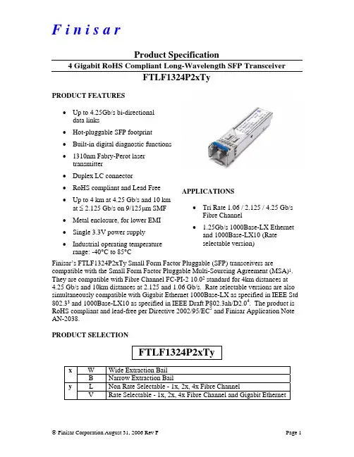
F i n i s a rProduct Specification4 Gigabit RoHS Compliant Long-Wavelength SFP TransceiverFTLF1324P2xTyPRODUCT FEATURES•Up to 4.25Gb/s bi-directionaldata links•Hot-pluggable SFP footprint•Built-in digital diagnostic functions •1310nm Fabry-Perot lasertransmitter•Duplex LC connector•RoHS compliant and Lead Free•Up to 4 km at 4.25 Gb/s and 10 km at ≤ 2.125 Gb/s on 9/125μm SMF •Metal enclosure, for lower EMI•Single 3.3V power supply•Industrial operating temperature range: -40°C to 85°CAPPLICATIONS•Tri Rate 1.06 / 2.125 / 4.25 Gb/s Fibre Channel• 1.25Gb/s 1000Base-LX Ethernet and 1000Base-LX10 (Rateselectable version)Finisar’s FTLF1324P2xTy Small Form Factor Pluggable (SFP) transceivers are compatible with the Small Form Factor Pluggable Multi-Sourcing Agreement (MSA)1. They are compatible with Fibre Channel FC-PI-2 10.02 standard for 4km distances at 4.25 Gb/s and 10km distances at 2.125 and 1.06 Gb/s. Rate selectable versions are also simultaneously compatible with Gigabit Ethernet 1000Base-LX as specified in IEEE Std 802.33 and 1000Base-LX10 as specified in IEEE Draft P802.3ah/D2.04. The product is RoHS compliant and lead-free per Directive 2002/95/EC5 and Finisar Application Note AN-2038.PRODUCT SELECTIONFTLF1324P2xTyx W Wide Extraction BailB Narrow Extraction Baily L Non Rate Selectable - 1x, 2x, 4x Fibre ChannelV Rate Selectable - 1x, 2x, 4x Fibre Channel and Gigabit EthernetI.Pin DescriptionsPin Symbol Name/Description Ref.1 V EET Transmitter Ground (Common with Receiver Ground) 12 T FAULT Transmitter Fault. Not supported.3 T DIS Transmitter Disable. Laser output disabled on high or open. 24 MOD_DEF(2) Module Definition 2. Data line for Serial ID. 35 MOD_DEF(1) Module Definition 1. Clock line for Serial ID. 36 MOD_DEF(0) Module Definition 0. Grounded within the module. 37 Rate Select Open or Low = High = 1.063 Gb/s or 2.125 Gb/s Fibre Channel, 1.25 Gb/sGigabit Ethernet (Low Bandwidth) 2.125 or 4.25 Gb/s Fibre Channel (High Bandwidth)4 8 LOS Loss of Signal indication. Logic 0 indicates normal operation.5 9 V EER Receiver Ground (Common with Transmitter Ground) 1 10 V EER Receiver Ground (Common with Transmitter Ground) 1 11 V EER Receiver Ground (Common with Transmitter Ground) 1 12 RD- Receiver Inverted DATA out. AC Coupled 13 RD+ Receiver Non-inverted DATA out. AC Coupled 14 V EER Receiver Ground (Common with Transmitter Ground) 1 15 V CCR Receiver Power Supply 16 V CCT Transmitter Power Supply 17 V EET Transmitter Ground (Common with Receiver Ground) 1 18 TD+ Transmitter Non-Inverted DATA in. AC Coupled. 19 TD- Transmitter Inverted DATA in. AC Coupled. 20 V EET Transmitter Ground (Common with Receiver Ground)1Notes:1. Circuit ground is internally isolated from chassis ground.2. Laser output disabled on T DIS >2.0V or open, enabled on T DIS <0.8V.3. Should be pulled up with4.7k - 10 kohms on host board to a voltage between 2.0V and 3.6V.MOD_DEF(0) pulls line low to indicate module is plugged in.4. For Rate Selectable version only: In accordance with SFF Committee SFF-8079 Draft, Rev.1.6,Table 3. Note that rate select can also be set through 2-wire bus in accordance with SFF-84726 at Bit 3, Byte 110, Address A2h (note: writing ‘1’ selects full bandwidth operation). Rate select is the logic OR of the input state of Rate Select Pin and 2-wire bus. Non Rate Selectable version can operate at 1x, 2x, 4x Fibre Channel independent of rate select pin setting.5. LOS is open collector output. Should be pulled up with 4.7k – 10 kohms on host board to a voltagebetween 2.0V and 3.6V. Logic 0 indicates normal operation; logic 1 indicates loss of signal.1234567891020191817161514131211Towards ASICTowards BezelPinout of Connector Block on Host BoardII. Absolute Maximum RatingsParameter SymbolMinTypMaxUnitRef. Maximum Supply Voltage Vcc -0.5 4.2 VStorage Temperature T S -40 85 °CCase Operating Temperature T OP -40 85 °CRelative Humidity RH 0 85 % 1III. ElectricalCharacteristics(T OP = -40 to 85 °C, V CC = 3.00 to 3.60 Volts)Parameter SymbolMinTypMaxUnitRef. Supply Voltage Vcc 3.00 3.60 VSupply Current Icc 200 300 mATransmitterInput differential impedance R in 100 Ω 2Single ended data input swing Vin,pp250 1200 mVTransmit Disable Voltage V D Vcc – 1.3 Vcc VTransmit Enable Voltage V EN Vee Vee+ 0.8 V 3Transmit Disable Assert Time 10 usReceiverSingle ended data output swing Vout,pp285 400 800 mV 4Data output rise/fall time ≤ 2.125 Gb/s t r, t f175 ps5Data output rise/fall time = 4.25 Gb/s t r, t f120 ps5LOS Fault V LOS fault Vcc – 0.5 Vcc HOST V 6LOS Normal V LOS norm Vee Vee+0.5 V 6Power Supply Rejection PSR100 mVpp7Deterministic Jitter Contribution ≤ 2.125 Gb/s RX Δ DJ51.7 ps8,9Total Jitter Contribution ≤ 2.125 Gb/s RX Δ TJ 122.4 ps 9Deterministic Jitter Contribution = 4.25 Gb/s RX Δ DJ25.9 ps8,10Total Jitter Contribution = 4.25 Gb/s RX Δ TJ61.2 ps10 Notes:1.Non condensing.2.AC coupled.3.Or open circuit.4.Into 100 ohm differential termination.5.20 – 80 %6.LOS is LVTTL. Logic 0 indicates normal operation; logic 1 indicates no signal detected.7.All transceiver specifications are compliant with a power supply sinusoidal modulation of 20 Hz to 1.5MHz up to specified value applied through the power supply filtering network shown on page 23 of theSmall Form-factor Pluggable (SFP) Transceiver MultiSource Agreement (MSA)1, September 14, 2000.8.Measured with DJ-free data input signal. In actual application, output DJ will be the sum of input DJand DJ.Δ9.As measured at 0.022 mW OMA.10.As measured at 0.048 mW OMA.IV. Optical Characteristics (T OP = -40 to 85 °C, V CC = 3.00 to 3.60 Volts)Parameter Symbol Min Typ Max Unit Ref.TransmitterOutput Opt. Power P OUT -3 dBm 1 Optical Wavelength λ 1260 1350 nm 2 Spectral Width σ Note 2 2 Optical Modulation Amplitude OMA 190 μW 2,3Optical Modulation Amplitude ≤ 2.125 Gb/sOMA 174 μW 2,3 Optical Rise/Fall Time = 4.25 Gb/s t r / t f 90 ps 4Optical Rise/Fall Time ≤ 2.125 Gb/st r / t f 160 ps 5 RIN -120 dB/Hz Deterministic Jitter Contribution = 4.25 Gb/s TX Δ DJ 28.5 ps 6 Total Jitter Contribution = 4.25 Gb/s TX Δ TJ59.8 ps Deterministic Jitter Contribution ≤ 2.125 Gb/s TX Δ DJ56.5 ps 6 Total Jitter Contribution ≤ 2.125 Gb/s TX Δ TJ119 ps Optical Extinction Ratio = 1.25 Gb/s ER 9 dB 7ReceiverReceiver Sensitivity = 4.25 Gb/s R SENSr 0.029 -18 mW dBm 89Receiver Sensitivity = 2.125 Gb/s R SENS2 0.015 -21 mW dBm 89Receiver Sensitivity = 1.06 Gb/s R SENS1 0.015 -22 mW dBm 89Receiver Sensitivity = 1.25 Gb/s R SENS1 -22 dBm 10,11 Stressed RX sens. = 1.25 Gb/s -14.5 dBm Receiver Overload Rx MAX 0 dBm Receiver Elec. 3 dB cutoff freq. 1500 MHz 11 Receiver Elec. 3 dB cutoff freq. 2500 MHz 12 Optical Center Wavelength λC 1260 1600 nm Return Loss 12 dB LOS De-Assert LOS D -19 dBm LOS Assert LOS A -30 dBm LOS Hysteresis0.5 dBNotes:1. Class 1 Laser Safety per FDA/CDRH and EN (IEC) 60825 regulations.2. Also specified to meet curves in FC-PI-2 10.0 Figures 18, 19, and 21, which allow trade-off betweenwavelength, spectral width and OMA. Rate selectable part is specified to meet IEEE Draft P802.3ah /D2.0 Figure 59-3.3. Equivalent extinction ratio specification for Fibre Channel. Allows smaller ER at higher averagepower.4. Unfiltered, 20-80%.5. Unfiltered, 20-80%.6. Measured with DJ-free data input signal. In actual application, output DJ will be the sum of input DJand DJ.Δ7. Applicable for Rate Selectable version only in low bandwidth mode.8. Measured with conformance signals defined in FC-PI-2 10.0 specifications. Value in OMA.Measured with PRBS 27-1 at 10-12 BER9. Measured with conformance signals defined in FC-PI-2 10.0 specifications. Represents sensitivitybased on OMA spec, as corrected to incoming Extinction Ratio of 13 dB (for example, at 5.75dBincoming extinction ratio, an OMA of 0.029 mW corresponds to -16 dBm sensitivity). Measured withPRBS 27-1 at 10-12 BER .10.Measured with PRBS 27-1 at 10-12 BER .11.Rate Selectable version in low bandwidth mode.12.Rate Selectable version in high bandwidth mode.V. General SpecificationsParameter SymbolMinTypMaxUnitsRef. Data Rate BR 1062 4250 Mb/sec 1Bit Error Rate BER 10-12 2Max. Supported Link Length on9/125 μm SMF @ 4X Fibre Channel L MAX1 4 km3Max. Supported Link Length on9/125μm SMF @ 1X and 2X Fibre Channel L MAX210 km3Max. Supported Link Length on 9/125μm SMF @ Gigabit Ethernet L MAX310 km3Notes:1.Gigabit Ethernet and 1x/2x/4x Fibre Channel compliant.2.Tested with a PRBS 27-1 test pattern.3.Distances are based on FC-PI-2 10.0 and IEEE 802.3 standards.VI. Environmental SpecificationsFinisar 1310nm Industrial Temperature SFP transceivers have an operating temperature range from –40°C to +85°C case temperature.Parameter SymbolMinTypMaxUnitsRef.Case Operating Temperature T op -40 85 °C Storage Temperature T sto -40 85 °CVII. Regulatory ComplianceFinisar transceivers are Class 1 Laser Products and comply with US FDA regulations. These products are certified by TÜV and CSA to meet the Class 1 eye safetyrequirements of EN (IEC) 60825 and the electrical safety requirements of EN (IEC) 60950. Copies of certificates are available at Finisar Corporation upon request.VIII. Digital Diagnostic FunctionsFinisar FTLF1324P2xTy SFP transceivers support the 2-wire serial communication protocol as defined in the SFP MSA1. It is very closely related to the E2PROM defined in the GBIC standard, with the same electrical specifications.The standard SFP serial ID provides access to identification information that describes the transceiver’s capabilities, standard interfaces, manufacturer, and other information. Additionally, Finisar SFP transceivers provide a unique enhanced digital diagnostic monitoring interface, which allows real-time access to device operating parameters such as transceiver temperature, laser bias current, transmitted optical power, received optical power and transceiver supply voltage. It also defines a sophisticated system of alarm and warning flags, which alerts end-users when particular operating parameters are outside of a factory set normal range.The SFP MSA defines a 256-byte memory map in E2PROM that is accessible over a2-wire serial interface at the 8 bit address 1010000X (A0h). The digital diagnostic monitoring interface makes use of the 8 bit address 1010001X (A2h), so the originally defined serial ID memory map remains unchanged. The interface is identical to, and is thus fully backward compatible with both the GBIC Specification and the SFP Multi Source Agreement. The complete interface is described in Finisar Application Note AN-2030: “Digital Diagnostics Monitoring Interface for SFP Optical Transceivers”.The operating and diagnostics information is monitored and reported by a Digital Diagnostics Transceiver Controller (DDTC) inside the transceiver, which is accessed through a 2-wire serial interface. When the serial protocol is activated, the serial clock signal (SCL, Mod Def 1) is generated by the host. The positive edge clocks data into the SFP transceiver into those segments of the E2PROM that are not write-protected. The negative edge clocks data from the SFP transceiver. The serial data signal (SDA, Mod Def 2) is bi-directional for serial data transfer. The host uses SDA in conjunction with SCL to mark the start and end of serial protocol activation. The memories are organized as a series of 8-bit data words that can be addressed individually or sequentially.For more information, please see the SFP MSA documentation1,6 or Finisar Application Note AN-2030.FTLF1324P2xTy transceivers can be used in host systems that require either internally or externally calibrated digital diagnostics.Please note that evaluation board FDB-1018 is available with Finisar ModDEMO software that allows simple to use communication over the 2-wire serial interface.IX. Mechanical SpecificationsFinisar’s Small Form Factor Pluggable (SFP) transceivers are compatible with the dimensions defined by the SFP Multi-Sourcing Agreement (MSA) 3.FTLF1324P2BTyFTLF1324P2WTyX. PCB Layout and Bezel Recommendations元器件交易网FTLF1324P2xTy Industrial Temp. SFP Product Specification – August 2006 F i n i s a rXI. References1.Small Form-factor Pluggable (SFP) Transceiver Multi-source Agreement (MSA),September 14, 2000.2.“Fibre Channel Physical Interface Specification (FC-PI-2 10.0)”. AmericanNational Standard for Information Systems.3.IEEE Std 802.3, 2002 Edition, Clause 38, PMD Type 1000BASE-LX.IEEE Standards Department, 2002.4.IEEE Draft P802.3ah/D2.0, Clause 59, PMD Type 1000BASE-LX10. IEEEStandards Department, 2003.5.Directive 2002/95/EC of the European Council Parliament and of the Council,“on the restriction of the use of certain hazardous substances in electrical andelectronic equipment.” January 27, 2003.6.“Digital Diagnostics Monitoring Interface for Optical Transceivers”. SFFDocument Number SFF-8472, Revision 9.3.XII.For More InformationFinisar Corporation1389 Moffett Park DriveSunnyvale, CA 94089-1133Tel. 1-408-548-1000Fax 1-408-541-6138sales@© Finisar Corporation August 31, 2006 Rev F Page 11。