press-fit-design-guide-line压接设计指南
- 格式:ppt
- 大小:3.36 MB
- 文档页数:23
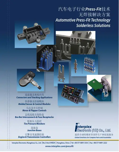
Global Solutions for Complex Parts and Assemblies连接器及堆栈应用 Connectors and Stacking Applications 传感器及控制模块Molded Sensor & Control Modules马达及开关控制Motor & Flapper Controls总线连接及保险盒Bus Bar Interconnects & Fuse Receptacles轮胎压力监控Tire Pressure Monitors 连接盒Junction Boxes 引擎及变速器控制Engine & Transmission Controllers::::::::::::::::::::::::::::::::::::::::::::::::::::::::::::::::::::::::::::::::::::::::::::::::::::::::::::::::::::::Interplex Electronic (Hangzhou) Co., Ltd. І No.3 Ave.8 HEDA І Hangzhou, China І Tel: +86 571 8691 3333 ІFax: +86 571 8691 2222/pressfi t提供全球性精密零部件生产和组装服务磷青铜 Phosphor Bronze 锡黄铜 Tinned Brass13% to 15%25% to 30%* 1.020 mm磷青铜 Phosphor Bronze锡黄铜 Tinned Brass 高导电合金 High Conductivity Alloy13% to 15%25% to 30%75% to 80%*1.486 mmCopyright © 2008 • Interplex Industries • /pressfi t: : : : : : : : : : : : : : : : : : : : : : : : : : : : : : : : : : : : : : : : : : : : : : : : : : : : :3.8mm 3.5mm1.2mm.80mm - Thick.64mm - Thick1.66mm怡得乐的Press-fit技术是一种无焊接连接Pin技术。

TITLEPAGEREVISION1 of 7AAUTHORIZED BYDATEPOWER EDGE CARD PRESS-FITJulia Wang Oct 07, 08CLASSIFICATIONUNRESTRICTEDCopyright FCI 1.0 OBJECTIVEThis specification provides information and requirements regarding customer application of PRESS FIT POWER EDGE CARD connector. This specification is intended to provide general guidance for process development. It is recognized that no single process will work under all customer applications and that customers will develop their processes to meet their needs.2.0 SCOPEThis specification provides information and requirements regarding customer application of PRESS FIT POWER EDGE CARD connectors.3.0 REFERENCE DOCUMENTSAny applicable product drawing (10075664-XXX) Product spec.: GS-12-459.4.0 GENERALThis document is meant to be an application guide. If information varies from that in the product drawings and specifications, the drawings take precedence.Paragraph TitlePage 1.0 Objective 1 2.0 Scope1 3.0 Reference Documents 1 4.0 General1 5.0 Application Information2 5.1General Product Information2 5.1.1 Terminal information 2 5.2 PCB Requirements4 5.3Customer Application Machines ( CAMS) 5 5.3.1 Insertion Tooling 5 5.3.2 Rework Tool7TITLEPAGEREVISION2 of 7AAUTHORIZED BYDATEPOWER EDGE CARD PRESS-FITJulia Wang Oct 07, 08CLASSIFICATIONUNRESTRICTEDCopyright FCI5.0 APPLICATION INFORMATION5.1 General Product InformationFigure 1: Press-fit Power Edge Card profile5.1.1 Terminal informationAn EON press-fit connection is achieved by mechanically inserting a pin into a plated thru hole (PTH). Theelectrical connection is maintained by the normal forces generated between the EON section to the PTH walls. There are a number of benefits in the use of press fit connections. First, using a press-fit connectioneliminates the need for soldering processes. Second, press-fit technology reduces rework concerns because a damaged connector may be pressed out and replaced with a new one (this process may be performed a maximum of two times in the same PCB).The EON was designed to meet the requirements for press-fit terminations according to MIL-STD-2166. Figure 2,3 illustrates a typical cross-section of EON pin after insertion into a PCB. This terminal may be used in a tin-lead, lead free PTH or in a copper OSP PTH. The OSP boards have special protective coatings to reduce oxidation. The specification requires the following:a. EON retention/insertion force should be checked on an 3.18±0.25mm min thick segment of FR-4glass/epoxy circuit board segment with a finished hole size of diameter 1.02±0.07mm drilled through. At a rate of 25±6 mm per minute:Insertion force no more than 4.54 Kgf (10Lbs) per pin. Retention force no less than 0.91 Kgf (2 Lbs) per pin.PTHEON tailTITLEPAGEREVISION3 of 7AAUTHORIZED BYDATEPOWER EDGE CARD PRESS-FITJulia Wang Oct 07, 08CLASSIFICATIONUNRESTRICTEDCopyright FCIb. PCB Hole Deformation Radius-Cross-section parallel to board surface(see figure 2). Photograph and measure the hole deformation (deformation on board material) radius at a point 0.010” from the surface, and at the center of the EON pin section. Include 10 holes. The average (of 10 holes) hole deformation radius shall be no greater than 0.0381mm (0.0015 inch) when measured from the drilled hole. The absolute maximum deformation radius shall not exceed 0.0508mm (0.002 inch). Reference MIL-STD-2166.c. PCB Hole Wall Damage-Cross-section perpendicular to the board surface(see figure 3), and through theEON section wear track. Photograph and measure the copper thickness remaining between the EON pin and the printed wiring board laminate. Include 10 holes. The minimum average (of 10 holes) copper thickness remaining between the EON pin and the printed wiring board laminate shall not be less than 0.00762mm(0.0003 inch). In addition there shall be no copper cracks, separations between conductive interfaces, or laminate-to-copper separations. Reference MIL-STD-2166.Figure 2: PCB Hole Deformation Radius-Cross-section parallel to board surface.Figure 3: PCB Hole Damage-Cross-section perpendicular to the board surface.TITLEPAGEREVISION4 of 7AAUTHORIZED BYDATEPOWER EDGE CARD PRESS-FITJulia Wang Oct 07, 08CLASSIFICATIONUNRESTRICTEDCopyright FCI 5.2 PCB RequirementsA press fit connection is a means of terminating connectors to printed circuit boards without going through a soldering operation. PCB layout is per customer drawing’s PCB recommended dimension. The features that are important to define on the printed circuit board when using press fit technology are:Drilled hole diameter Plated hole diameter Plating type in thru holePrinted circuit board thicknessLand/pad sizeCollectively, these features influence the reliability of the termination as well as the force required to apply theconnector to the printed circuit board. The recommended values are shown in Table 1, and a sketch showing these features is shown in Figure 4.Table 1: Recommended feature sizes for PF POWER EDGE CARD PCB’s.DimensionFeaturemmDrill Hole diameter 1.151+/-0.025 Plated hole diameter1.02/-0.07 copper plating on hole wall0.051+/-0.025 Tin/Lead or Tin plating (optional) 0.007Land/Pad size 1.727+/-0.064TITLEPAGEREVISION5 of 7AAUTHORIZED BYDATEPOWER EDGE CARD PRESS-FITJulia Wang Oct 07, 08CLASSIFICATIONUNRESTRICTEDCopyright FCIFigure 4: Critical features of PCB design for PF POWER EDGE CARD connector.5.3 Customer Application Machines ( CAMS)5.3.1 Insertion ToolingPRESS FIT POWER EDGE CARD connector can be installed with any standard press as long as it capable of applying force as specified earlier in this document. A flat-rock press can be used as a top tool for 31(x2), 19(x2),. Make sure the backup fixture does not interfere with pins protruding through the PCBFlowing are the recommended insertion tooling design:TITLEPAGEREVISION6 of 7AAUTHORIZED BYDATEPOWER EDGE CARD PRESS-FITJulia Wang Oct 07, 08CLASSIFICATIONUNRESTRICTEDCopyright FCI6.175mmTITLEPAGEREVISION7 of 7AAUTHORIZED BYDATEPOWER EDGE CARD PRESS-FITJulia Wang Oct 07, 08CLASSIFICATIONUNRESTRICTEDCopyright FCI 5.3.2 REWORK TOOLINGPress fit POWER EDGE CARD connector can be reworked when the defected connector is pressed out and replaced with a new one. The recommended rework tool is designed as the figure 5. If want to get the detailed design, please contact to FCI engineers. Figure 5 --- Recommended connector remove fixtureRevision RecordREVISION PAGE DESCRIPTIONECN DATE A ALL NEW RELEASED DG08-028010/07/08Ø。
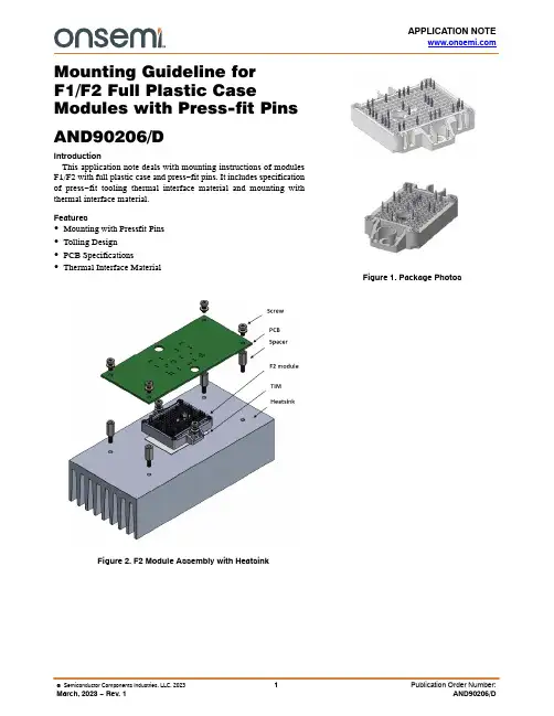
APPLICATION NOTE Mounting Guideline forF1/F2 Full Plastic Case Modules with Press-fit Pins AND90206/DIntroductionThis application note deals with mounting instructions of modules F1/F2 with full plastic case and press−fit pins. It includes specification of press−fit tooling thermal interface material and mounting with thermal interface material.Features∙Mounting with Pressfit Pins∙Tolling Design∙PCB Specifications∙Thermal Interface MaterialFigure 2. F2 Module Assembly with HeatsinkFigure 1. Package PhotosSpecification of PCBMinimum PCB thickness is 1.6 mm. Solder mask is recommended on both sides of the PCB. Recommended PCB hole plating options include immersion tin, immersion silver, electroless nickel immersion gold ENIG), and organic solderable preservative (OSP). HAL plating is not recommended. For PCB specifications please see Table 1.Figure 3. PCB Hole DimensionsTable 1. PCB SPECIFICATIONS FOR F1 AND F2MODULES WITH 1.2 MM PRESS −FIT PINSMin.Typ.Max.Initial Drilled Hole Diameter Ø[mm]1.12 1.15Cu Thickness in the Hole [m m]2550Sn Thickness [m m] (Chemical Tin)15Final Hole Ø [mm]1 1.09Annular ring [m m]200Thickness of Conductive Layer [m m]3570−105400Board Thickness [mm]1.6Design Restrictions within Mounting AreaPCB bending during the press −in process causes mechanical stress to other PCB components, such as capacitors and resistors. Experiments to verify a safe minimum distance between passive components and the plated through hole were conducted with FR4 PCB. V arious sizes (0603, 0805, 1206, 1210, 1812, and 2220) of mechanically sensitive components were evaluated. Based on experimental results, the recommended minimum space between center of the plated through hole and the edge of the component is 4 mm, as shown in Figure 4.Figure 4. PCB Layout RestrictionsPCB Fixing and DimensionsSpacers should be used to fix the PCB to the heatsink.Number of space posts is not given. Space posts positions should be designed symmetrically, weight of the PCB components should be considered. PCB bending or flexing should be avoided. Distance from the space post to the module (dimension x) is recommended to be at least 10 mm from module outer edges.Figure 5. Module Fixed on a HeatsinkLength of the space posts should match the length of press −in tool distance keeper – see section Press −in tool for F2 package.Recommended length of the space post is 12.4 mm + 0 mm −0.05 mm. An air gap may be present between the module and PCB (as on Figure 5), this airgap allows tolerance of the module case.Press −in ProcessThe press −fit connection generates a good electrical, and strong mechanical connection between the module and the PCB. This section deals with the mounting process to achieve suitable press −fit connections here are several types of presses available: from simple toggle presses to the automated pneumatic presses shown in Figure 6.Figure 6. Press −in Machine ExampleIf possible, monitor the press −in/press −out distance,speed, and force to achieve mechanical stability and high reliability of the press −fit connection. The travel distance during the press −in process should be controlled to ensure that the press −fit zone of the pins sits properly in the plated through hole. The speed also influences the quality of the press −fit connection; therefore, speed recommended by IEC standard should be applied.Figure 7. Pressfit Tool for F2 ModuleGeneral Press −in ProcessUse of tooling with distance keeper is recommended.Figure 8. Shows the general sequence of press in procedure.Press −in procedure. The press −in tool is comprised of two parts: the upper press −in tool is flat (or with special design for modules with TIM. Please see Press −in tool for module with PCM section) to contact with the module backside evenly and the lower press −in tool has engraved spaces to accommodate the press −fit pins and PCB components. The two parts of the tool need to be aligned to each other. In the first step of the assembly, the printed circuit board is placed on the alignment pins of the lower part of the press −in tool (a). Then, the module is placed on top of the printed circuit board using the alignment pins (b).Figure 8. Press −in ProcessIt is necessary to check if the module and the printed circuit board are in alignment. In the next step, the press−in force is applied via the upper part of the press−in tool to the backside of the module evenly. The module should be pressed−in with a speed of 25~50 mm/min until the distance keepers of the upper tool touch the PCB while press−in distance and force are monitored at the same time (c). It is required to adjust the traveling distance of the press to avoid damages to the module case due to pressure being applied.A simple manual press does not use a distance sensing system, so a distance keeper should be designed on the press−in tool to terminate press−in process appropriately. When the distance keeper contacts the surface, press−inforce rises sharply, and the press−in process can be terminated by reaching the limit of the press−in force. The distance keeper should be designed to avoid the collision with other PCB components.Figure 9. Distance Keeper of the Upper Tool Design The total press−in force is the result of the number of pins in a module, multiplied with the force required for a single pin. Press−in forces lower than 40 N/pin mean that press−fit pin may have a less secure connection in the plated through hole. The primary reason for the low press−fit force is that the diameter of plated through hole is too large for the press−fit pins. Press−in forces higher than 80 N/pin can cause mechanical damage to the press−fit terminal, the PTH, or to the tracks on the PCB. The recommended press−in speed ranges from 25 mm/min to 50 mm/min in accordance with the recommendations in IEC 60352−5.Figure 10. PCB Thickness SpecificationThe press−fit pins must be pressed into the holes of the PCB to the correct depth. The center of the press−fit zone has to be at least 0.5 mm below the top surface and at least 0.5mm above the bottom surface of the PCB (Figure 10).Figure 11. Force vs. Distance during PressfitProcessForce measured in a module is a sum of all pins being pressed at once (Figure 11).Force measurement per one pin was conducted, the press−fit pin was mounted in 1.6 mm thick PCB with chemical Sn surface finish. Test conditions and PCB specification are compliant with IEC 60352−5.Table 2. SINGLE PRESS−FIT PIN TESTPress−in Force Press−out ForcePCB hole f0.98 –1.02 mmf1.11 –1.12 mmf0.98 –1.02 mmf1.11 –1.12 mm(min)(max)(min)(max) Minimum49.8 N40.9 N29.4 N38.3 N Mean55.9 N47.4 N40.5 N48.2 N Maximum62.1 N57.1 N48.0 N65.9 N Samplesize20201920Press−in Tool for Module with PCMTo prevent damages on PCM peripheral spacers and point spacers are required. This spacers should not touch PCM on the DBC. 0.4 mm is recommended for the height of spacers. Distance keeper of the press−in tool needs to be 0.4 mm taller than no PCM cases.Figure 12. Press−fit Tool for F2 Module with PCMFigure 13. Point Spacer Alignment with PCMPeripheral spacer and point spacer prevent pre −applied PCM from being deformed or damaged during press −in process. Peripheral spacer distributes mechanical stress by press −in process over the edge of DBCPress −out ProcessIn some situations, it is necessary to remove power modules from the PCB. It is possible to disconnect the contact between module pins and PTH. The press −out process can be performed with the same equipment used in the press −in process. Careful handling in the press −out process is essential to avoid mechanical damage to both the module and the PCB. PCB can be re −used once with a new module. Please note: in case a module which was pressed out of a PCB should be used again, it is necessary to solder the module to the PCB; this is because the press −fit zone will remain deformed after the press −out process. An additional press −in cycle will result in low holding forces between the press −fit pin and PCB hole.Figure 14. Press −out ToolFigure 15. Press −out Process of Power Module Heatsink SpecificationThe following surface qualities are required for the heatsink to achieve a good thermal conductivity, according to DIN 4768−1. Roughness (Rz) should be 10 m m or less and flatness, based on a length of 100 mm, should be 50 m m or less. The heatsink should have no contamination,unevenness, and burrs on the surface contacting the module.The interface surface of the heatsink must be free of particles and contamination. Avoid handling the heatsink surface with bare hands or contacting any foreign materials.If it is necessary to remove contamination from heatsink,cleaning can be accomplished using dry cloth soaked with solvent, such as isopropyl or ethylene alcohol.Figure 16. Heatsink Surface SpecificationThermal GreaseThermal grease can be applied to the heatsink or the module substrate using a rubber roller or spatula or by screen printing. Alternatively, apply thermal paste by screen printing, for example using a honeycomb pattern. The recommended thermal paste thickness is 80−180 m m.Thickness of the TIM layer more than this recommendation will unnecessarily increase thermal resistance. When applying thermal grease, the material must be applied uniformly on the whole surface which is in contact to the module substrate surface. If the module is re −mounted,surfaces should be cleaned, and TIM needs be applied again.Pre−applied Phase–Change MaterialModules can be pre−applied with phase−change material. Typical thickness of the TIM layer is 160m m and its thermal conductivity is 3.4 W/mK.Figure 17. Tim Pattern Example on F2 ModuleIt comes pre−applied on the DBC surface ready to be mounted on the heatsink. The honeycomb pattern allows the press tool to touch copper DBC and allows PCM to spread on a whole surface. For proper TIM spreading in application, TIM spreading temperature must be achieved on the TIM material, this temperature is specified as minimum 45︒C. For best spreading results it is recommended to apply 80︒C for 20 minutes.Screw SpecificationWhen using screws with flat washers:∙Metric screw: M4 (recommended screw type DIN7984)∙Flat washer: D = 8 mm ISO 7092 (DIN 433)∙Spring washer: D = 8 mm DIN 127 or DIN 128∙Mounting torque: 1.6−2.0 Nm∙Screw holes on heatsink need to be countersunk. A torque wrench shall be used to tighten the mounting screws at the specified torque. Excessive torque may result in damage or degradation of the device. The inaccuracy of torque wrench tightening method can range up to ±12%. This must be considered to prevent over−tightening the fastener. Due to excessive temperature fluctuations washers should be used to prevent the loosening of the screws. After accurate tightening of the screws the spring washer exerts a constant force on the joint. The flat washer distributes this force on the plastic surface. When using screws with pre−assembled washers: Screws with pre−assembled washers (SEMS or kombi screws) combine the screw and the washers into a single component. These screws eliminate the need to slip the washers into place by hand, boosting the speed and efficiency of the assembly process. The specifications of these screws are provided below:∙Screw size: M4 according to DIN 6900 (ISO 10644; JIS B1188)∙Flat washer: According to DIN 6902 Type C (ISO 10673 Type S; JIS B1256) Washer outer diameter: 8mm diameter can be fitted onto the module ∙Split lock spring washer: According to DIN6905 (JIS B1251)∙Mounting torque range: 1.6−2.0 Nm∙Recommended insertion of screw thread in the heatsink is 6mm.Methods of Screw ClampingThere are two recommended screw clamping methods which apply to all modules. The F1 module is used as an example. Figure 18 describes one method for fastening the module to the heatsink. Fasten two screws simultaneously to prevent tilting or rising of one side of module during fastening. Electric screwdrivers can tighten the screws with the specified torque. Screw holes on heatsink need to be countersunk. If method 1 cannot be applied, the method as described in Figure 19 is also acceptable. Fasten the first screw loosely to prevent tilting or rising of the module (step1). Then insert the second screw with final torque to be fully tightened with the heatsink (step 2). Finally, apply full torque to the first screw for solid tightening with the heatsink. For F1/F2 packages using metal clips, the torque is between 1.6−2.0 Nm using M4 screws.Figure 18. Fixing Screws on the HeatsinkFigure 19. Fixing One after One for Power ModuleAssembly of Multiple Modules on the PCB and HeatsinkThe overall structure of the mounted module should be considered. If the PCB is large and heavy with other components assembled to it, there is some risk the PCB can bend, creating mechanical stress to the module and the PCB. When multiple modules are applied to the same PCB, height tolerance between modules can result in the mechanical stresses on the board and modules. To reduce stress, space posts should be added on the heatsink, as illustrated on figure 19 to prevent movement of the PCB. The recommended height of the space posts is 12.4 (+0/−0.1) mm. The effective distance between center of stand−off and the space post (=X) is 50 mm minimum. If distance keepers are used during the press−in process, resulting in tighter height tolerances; distances between the stand−off of the case and the space post (= X) smaller than 50 mm can be used. Figure 19 shows the assembly procedure when space posts are used and the overall assembly structure: Modules are first pressed into the PCB following the recommendations introduced in Section “Heatsink Surface” before heatsink mounting. Maintaining tight height tolerances between module and PCB is important. Next, the thermal interface material is applied. Then the modules and the PCB are placed on the heatsink (a). Then the module is mounted onto the heatsink via the module plastic clamp. Finally, the PCB needs to be fixed on the space posts (c).Figure 20. Assembling Multiple Modules on a PCB Handling of PCM Pre−applied ModuleDuring a transport and storage of the modules extreme thermal and mechanical shock should be avoided. The tray is designed to prevent direct contact to the PCM layer of the module substrate as shown in the Figure 21. PCM_ pre applied modules should be stored in this tray box before its use. Table 3 shows recommended storage conditions. Table 3. RECOMMENDED STORAGE CONDITIONS FOR MODULES WITH PCMStorage temperatures10 – 40 ︒CHumidity condition10 < RH < 55%Time Max 12 monthsPCM printing layer should be treated as a functional area of the module and be protected from damage or removing when handling or mounting. PCM pre−applied module is delivered in a tray box with a tight cover.Figure 21. Modules in a Transport Tray BoxIt is recommended to open the cover carefully side−by side to prevent mechanical damage to the PCM layer. Also during the assembly process attention is needed not to touch the PCM layer directly. If the PCM layer is contaminated or more thant 10% of the entire printed area is damaged, then it is recommended to remove the PCM layer according to instructions stated below. In case of rework prior to operation of modules, standard PCB / heat sink disassembly process can be applied. If the module was operated and the PCM melted and distributed already, then bond strength between heat sink and the module may be strong, and the module cannot be easily removed from the heatsink. In such cases it is recommended to use a knife to detach the module or apply some heat (45−60︒C) to re−melt PCM to detach the module easily. Use a soft plastic scraper to remove the PCM layer from the module back side and heat sink. For the removal of remaining PCM residues it is recommended to use microfiber cloth and isoprophyle alcohol.PUBLICATION ORDERING INFORMATIONTECHNICAL SUPPORTNorth American Technical Support:Voice Mail: 1 800−282−9855 Toll Free USA/Canada Phone: 011 421 33 790 2910LITERATURE FULFILLMENT :Email Requests to:*******************onsemi Website: Europe, Middle East and Africa Technical Support:Phone: 00421 33 790 2910For additional information, please contact your local Sales Representative。


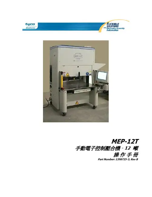
MEP-12T 手動電子控制壓合機 - 12 噸操作手冊Part Number: 1398725-3, Rev B介紹 (5)關於這個手冊 (5)安全 (5)停機標簽 / 警示標簽 (5)安全蓋 / 防護罩 (6)雷射感應器 (6)緊急關閉機器(EMO) / ESTOP (7)光柵 (7)光柵手控鍵開關 (7)氣動系統 (7)萬向滑輪 (8)防震措施 (8)骨架結構及重量分佈 (8)安裝 (8)拆箱 (8)開始組裝 (9)設備標示牌 (10)電氣供應回路 (10)壓縮空氣的供應 (10)壓合機概觀 (11)目的 (11)能力 (11)選擇性配件 (13)觸控式SVGA 顯示器 (13)板厚測量 (13)SPC (Statistical Process Control)統計過程控制 (13)電腦條碼機 (13)雷射定位器 (13)光柵 - CE 認證 (13)數位彩色相機 (13)彩色印表機 (13)機器特性與結構 (14)配置 (14)操作 (15)開始起動 (15)起動電源 (15)操作者介面 (16)開機 (16)使用者存取 (17)選擇PC板 (18)PC板的運作 (18)運轉畫面按鈕 (19)畫面上PC板的配置 (22)開始壓合 (22)第一件物品確認信號(First Article Signoff) (23)中斷壓合循環(Interrupting the Pressing Cycle) (23)變更壓合順序(Changing the Pressing Sequence) (23)有關電路板、連接器、治具及程式的錯過狀況 (23)壓合治具PRESSING TOOLS (25)支撐固定裝置 (平臺 / 支撐座) (25)編程和數據輸入 (25)治具編輯器 (26)目的 (26)進入 (26)連接器編輯器 (28)目地 (28)進入 (28)模態編輯器 (30)目地 (30)說明 (30)壓合數據編輯器 (36)PRESS SEQUENCE 壓合順序 (38)SPC 選擇 (39)Process Data程序數據 (40)CPK (Process Capability)加工能力 (40)X-Bar (Process Average)加工的平均數 (40)Std Dev. (Standard Deviation)標準偏差 (40)UCL (Upper Control Limit)控制上限 (40)LCL (Lower Control Limit) 控制下限 (40)VCL (Variability Control Limit)變化性控制限度 (40)Point Data 點數據 (40)Options選擇 (41)Range Bars (41)Control Limits控制限度 (41)Spec. Limits規格限度 (41)Grid 網 (41)Shaded 色差 (41)Thick Lines 粗線 (41)Print 列印 (41)維修功能(公用的) (42)機器記錄 (42)Error Log 錯誤記錄 (42)User Log 使用者記錄 (42)Joystick 控制桿 (44)Analog Inputs 類比輸入 full force range (44)Points 點 (45)Control 控制 (45)Calibration校正 (46)Tools工具 (46)Machine Zero機器歸零 (46)輸入/輸出螢幕 (47)Servo Terminal伺服終端 (48)伺服參數 (49)Setup Parameters (51)Machine Operation (51)Load Cells (52)Save (52)Cancel (52)使用 (53)預防保養 (54)Accessing the Press Head (54)Cleaning (54)Inspection (54)Lubricating (54)Z Axis Rods (54)Z Axis Screw (54)Torquing Critical Bolts (54)Clean Water Trap In Air System (54)PM Schedule (55)Load Cell Calibration (56)Calibration Procedure for Initial Setup of MEP-12T: (56)Load Cell Calibration (58)Balance Load Cells (59)Calibrate the load cells (60)APPENDIX A - SPARE PARTS LIST (62)APPENDIX B – FEATURES & SPECIFICATIONS (63)APPENDIX C: ELECTRICAL & MECHANICAL SCHEMATICS: (64)介紹關於這個手冊這個手冊包含對於12 公噸手操作電動壓合機(MEP-12T)的安裝, 安全, 操作, 和保養程序。

Press fit technologyPress fit technology – as one of the most important manufacturing technologies – has become well established in production processes of the electronic industry. Based on the norm IEC 60352—5 press fit technology is recorded and appraised in a qualitative manner。
(定性方式)Press fit technology is based on the fundamental method of pressing a contact pin (with or without an elastic press fit zone) using pressure in a metalized borehole(金属化孔), or as the case may be,a feed through(连通)。
Due to the extensive range of the contact pin and the smaller bore diameter of the metalized borehole, Press fit technology – as one of the most important manufacturing technologies – has become well established in production processes of the electronic industry. It results in a gas proof(气密),electric conductible connection(导电连接). On suitable surfaces we talk about a cold shut and so an inter metallic connection。

6Fine-fit DIN Connectors with W-shaped Pins XC5■XC5 AccessoriesHandleHandle wheel Pressure headerPress-fit Tool (XY2D-1005)•Hand-operated tool designed espe-cially for mounting Fine-fit Connectors to a board.•Hand-operated for ease and safety.•The Press-fit T ool User’s Manual must be ordered separately.SpecificationsModelApplicable Connectors XC5@-@@@P Fine-fit Max. pressure 2 tStroke (max.)8 mm (handle)283 mm (handle wheel)Weight 80 kgBase area500 mm × 530 mmModelXY2D-1005For plugsFor socketsContact Repair Tools•The tool works on top of the Connector.•This tool is used for correcting mistakes made with the Press-fit Tool. (plugs only)•For details on use, see the Fine-fit Connector Press-fit T ool User’s Manual. The User’s manual must be ordered separately.For PlugsFor SocketsRowsNo. of contactsModel Double rows (XC5E)32XY2D-100764XY2D-1006100XY2D-1035Triple rows (XC5G)48XY2D-100996 (64)XY2D-1008Rows No. of contactsModel Double rows (XC5B)32XY2D-101164XY2D-1010100XY2D-1036Triple rows (XC5D)48XY2D-101396 (64)XY2D-1012Support Block and Plungers•The Support Block and Plungers (2) are set on top of the base board.•The Support Block is used to protect the fine-fit pins while the Press-fit T ool is being used.•The Plunger is inserted into the mounting holes. It functions as a posi-tioner for the Connector and cushions the Contact Repair Tool.Support BlocksNote:Cut the XY2D-1014 when using Double-row Connectors with 100 or 32 contacts.Cut the XY2D-1015 when using T riple-row Connectors with 100 or 32 contacts (no center row).PlungersRowsNo. of contactsModelDouble rows 64XY2D-1014Triple rows96XY2D-1015Applicable board thickness Model 1.6 to 3.2 mmXY2D-1017Pressure Tool header Contact Repair ToolFine-fit Connector Circuit board (blackplane)PlungerSupport BlockBase boardSetting the Repair Tool, Support Block, and Plunger•Base board is not supplied by OMRON.•The base board including the Support Block and Plunger are collectively called the Support Assembly.•Place the circuit board on top of the Support Assembly and place the whole thing on the Press-fit Tool.•Insert the Fine-fit Connectors into the board one at a time by moving the Sup-port Assembly left and right.。
MEP-12T手动电子控制压合机 - 12 吨操作手册Part Number: 1398725-3, Rev B 介绍 ..................................................................................................................................................................关於这个手册 ..............................................................................................................................................安全 (1)停机标签 / 警示标签 ..................................................................................................................................安全盖 / 防护罩 ...........................................................................................................................................雷射感应器 ..................................................................................................................................................紧急关闭机器(EMO) / ESTOP ....................................................................................................................光栅 ..............................................................................................................................................................光栅手控键开关 ......................................................................................................... 错误!未指定书签。