外转子直流无刷电机CW63BLW33-40L220-00规格说明书(20151024)
- 格式:pdf
- 大小:116.68 KB
- 文档页数:3
CW系列电涡流测功机主机使用说明书豫制03000011号凯迈 (洛阳) 机电有限公司(原洛阳南峰机电设备制造有限公司)目录1、引言 (4)1.1 概述 (4)1.2 电涡流测功机型号含义及技术参数 (5)2、电涡流测功机的主机结构和工作原理 (6)2.1电涡流测功机的工作原理 (6)2.2 电涡流测功机的功率计算 (6)2.3 电涡流测功机的主机结构 (6)2.4 电涡流测功机的报警装置 (7)3、电涡流测功机的主要技术指标 (8)4、电涡流测功机的布置和安装 (8)4.1 电涡流测功机的工作条件 (8)4.2 电涡流测功机的布置 (8)4.3 电涡流测功机的安装 (8)5、电涡流测功机测功机的冷却 (11)5.1.电涡流测功机的冷却原理 (11)5.2 电涡流测功机对冷却水水质的要求 (11)5.3 电涡流测功机冷却水水量的确定 (11)6、电涡流测功机的润滑 (12)6.1电涡流测功机的油润滑 (12)6.2电涡流测功机的脂润滑 (13)6.3电涡流测功机摆动轴承的润滑 (13)7、电涡流测功机的校准和调节 (14)7.1 电涡流测功机的静校 (14)7.2 电涡流测功机的灵敏度检查 (18)8、电涡流测功机的运输和维护 (18)8.1 电涡流测功机的贮存 (18)8.2 电涡流测功机的运输 (18)8.3 电涡流测功机的检查和维护 (19)9、电涡流测功机的配套 (19)10、电涡流测功机主机的常见故障和排除方法 (20)11、电涡流测功机新润滑系统的使用和维护 (21)12、电涡流测功机的图册部分 (22)图1(a)~(b)电涡流测功机的主机结构 (23)图2(a)~(o)电涡流测功机的机械特性曲线 (25)图3(a)~(m)电涡流测功机的外形尺寸 (40)图4(a)~(i)电涡流测功机的接线图 (53)图5 电涡流测功机进水温度、使用功率和水量之间的关系 (62)1、引言1.1 概述我公司根据德国策尔纳(ZÖLLNER)公司专有技术生产的CW系列电涡流测功机,具有低惯性、高精度、高稳定性和结构简单、维修方便、自成系列并适用于操作控制自动化等优点。

空模无刷马达电子调速器(ESC )说明书 HW-SM003DUL-20130709page 1鸣叫提示音符“ 123”,表感谢您购买本产品!无刷动力系统功率强大,错误的使用可能造成人身伤害和设备损坏。
为此我们强烈建议您在使用设备前仔细阅读本说明书,并严格遵守规定的操作程序。
我们不承担因使用本产品或擅自对产品进行改造所引起的任何责任,包括但不限于对附带损失或间接损失的赔偿责任。
产品特色1. 所有器件均为原装正品,确保电调具有一流品质和极高的可靠性。
2. 具有强大的耐流能力。
3. 具备输入电压异常保护、电池低压保护、过热保护、油门信号丢失保护等多重保护功能。
4. 具有普通启动、柔和启动、超柔和启动三种启动模式,兼容固定翼飞机及直升机。
5. 可设定油门行程,兼容各种遥控器。
具备平滑、细腻的调速手感,一流的调速线性。
6. 最高转速可以达210000 RPM (2极马达)、70000 RPM (6极马达)、35000 RPM (12极马达)。
产品功能简要说明(黑体字为出厂默认值) 1. 刹车设定:无刹车/有刹车。
2. 电池类型:Lipo (锂电池)/ NiMH (镍氢)。
3. 电池低压保护模式:逐渐降低功率/立即关闭输出。
注:低压保护时,将油门摇杆拉到最小油门的位置后即可重新启动马达,但因为此时仍处于低压状况,所以功率输出较小。
4.低压保护阈值:低/中/高。
1) 当电池类型设定为Lipo 电池时,电调自动判断锂电节数,低/中/高情况下每节电池的截止电压分别为:2.85V/3.15V/3.3V 。
例如使用3节锂电,设定为中截止电压,则低压保护阈值为:3.15*3=9.45V 。
2) 当电池类型设定为镍氢电池时,低/中/高情况下截止电压为开机时输入电压的0%/50%/65%。
0%意味着不进行低压保护。
例如:使用6节镍氢电池,充满时电压为 1.44*6=8.64V ,当设定为中截止电压时,则截止电压阈值为:8.64*50%=4.3V 。

CDV2sX-32旋钮式电动机断路器CDV2sX-32旋转式电动机断路器1-脱扣测试孔2-透明盖3-整定电流范围4-整定旋钮5-进线端6-顶辅助触头保护盖7-旋钮8-闭锁装置.1.16I>>TEST0.1-0.16A9-指示窗10-出线端11-螺钉拧紧扭矩12-额定绝缘电压Ui、 冲击耐受电压Uimp13-产品规格14-技术参数15-认证标识及符合标准CDV2sX-32CDV2sX-32表3 辅助触头基本参数名称型号额定绝缘电压U i V额定冲击耐受电压Uimp kV 约定自由空气发热电流Ith使用类别额定工作电压Ue V 额定工作电流Ie A 正装 辅助触头组25042.5AC-1524248 1.2511012300.5DC-13241480.3侧装 辅助触头组69066AC-15486110 4.5230 3.3380 2.2DC-132464852200.5产品附件辅助触头基本参数见表3,其他参数见表4。
表4 辅助触头其他参数与性能序号内容参数1外壳防护等级IP202配用熔断器型号gG 、RT36-003配用熔断器额定电流(A ): 4: 104额定限制短路电流Iq(kA)15导线(导线/导电排)插入端子之前应剥掉绝缘长度(mm )86导线(导线/导电排)截面积mm20.75~0.257允许夹入导体(导线/导电排)的最大根数28接线端紧固螺钉(或螺栓)大小M 3.59接线端紧固螺钉拧紧力矩(N·m )1.2最大安装数量12AEV2s11AEV2s20ANV2s11ANV2s20AEV2s AUV2s断路器瞬时电磁脱扣动作特性应符合表7的规定。
表7瞬时脱扣特性序号试验电流起始状态规定时间预期结果10.8Ii冷态t≥0.2s不脱扣2 1.2Ii冷态t<0.2s脱扣启动时间-电流特性曲线。
20 °C 时,设定电流倍数对应的平均动作时间时间(s)x 设定电流 (Ir)1从冷态开始,3 极2从冷态开始,2 极3从热态开始,3 极内部电气原理示意图23.845.331.589.5max13.513.517.49.49.418.437.4 ANV2s11, ANV2s20AUV2s,ASV2s断路器工作原理保护与协调短路电流小于或等于断路器的额定极限短路分断能力时,应由断路器承担保护;当短路电流大于断路器的额定极限分断能力时,则由熔断器或断路器进行保护。
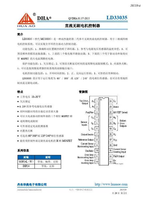
丹东华奥电子有限公司简介LD33035(替代MC33035)是一种高性能的第二代单片无刷直流电机控制器。
用于三相或四相电机控制系统,可以实现全开环的全部动力控制功能。
功能包括:1、准确转动位置测序的转子译码器;2、参考与电源电压传感器的温度补偿;3、可预设频率的锯齿波振荡器;4、上部的三个集电极开路驱动器;5、下部的三个用于驱动功率场效应管MOSFET 的大电流图腾柱电路。
保护功能包括:1、欠压锁定;2、可预设关断延迟时间的逐周期电流限制模式;3、内部热关断;4、可以连接到微处理器控制系统的故障输出端口。
电机控制功能包括:1、开环时间控制;2、正、反向运行控制;3、可控的启用和制动。
LD33035设计用于运行角度为60°/300°或120°/240°的电相位传感器,也可以有效地控制直流无刷电动机。
特点管脚图●工作电压10~30V ●欠压锁定●6.25V 的参考电源电压传感器●闭环伺服应用的全接近误差放大器●可以大电流驱动控制外部的三个相位MOSFET 桥●逐周期电流限制●可外部设定电流检测基准●内置热关断●可选的60°/300°或120°/240°相位传感器●能有效控制外部无刷直流电机的H 桥MOSFET系列信息封装说明SOP24L (W )管装,编带,无铅DIP24管装,无铅直流无刷电机控制器管脚功能描述丹东华奥电子有限公司功能示意图丹东华奥电子有限公司极限参数丹东华奥电子有限公司电参数(V CC=V C=20V,R T=4.7k,C T=10nF,T A=25℃,除非另外说明)丹东华奥电子有限公司CC C T T A注:1、输入共模电压或输入信号电压不应超过-0.3V。
2、调节电压不得超过−0.3至V REF范围。
丹东华奥电子有限公司介绍LD33035(替代MC33035)是一种单片的直流无刷电机控制器,它包含了开环控制的三、四相电机控制系统所需的全部功能。

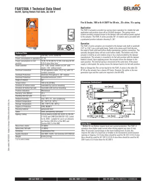
† UL File XAPX.E108966Fire & Smoke, 180 in-lb @ 350°F for 30 min., 25 s drive, 15 s spring ApplicationThe FSAF..A actuators provide true spring-return operation for reliable fail-safe application and positive close-off on UL555S dampers. The spring-returnsystem provides constant torque to the damper with and without power applied to the actuator. The FSAF..A series provides 95° of rotation and is provided with a graduated position indicator showing 0...95°.OperationThe FSAF_A series actuators are mounted to the damper axle shaft or jackshaft (1/2” to 1.05”) via a cold-weld clamp. Teeth in the clamp and V-bolt dig into the metal of both solid and hollow shafts maintaining a perfect connection. The specially designed clamp will not crush hollow shafts. The bottom end of the actuator is held by an anti-rotation strap or by a stud provided by the damper manufacturer. The actuator is mounted in its fail safe position with the damper blade(s) closed. Upon applying power, the actuator drives the damper to the open position. The internal spring is tensioned at the same time. If the power supply is interrupted, the spring moves the damper back to its fail-safe position.Note on linkage kits.The correct leg kit for the FSAF_A series is the older ZG-AF US as the actuator has a classic AF frame. However, the spline is the new generation type and the crank arm required is the KH-AFB.Safety Notes* Neither UL nor Belimo require local over-current protection. The FSAF_A actuators draw higher peak current when driving against any type of stop. After 10 seconds current drops to the lower holding level. If used, thisrequires the value of a local fuse or breaker to be increased to avoid nuisance opening or tripping. A 2 A slow blow should be used for AC 24 V. A 0.5 A slow blow should be used for AC 120 V. A 0.25 A slow blow should be used for AC 230 V and a 0.3 A slow blow for AC 208 V.FSAF230A.1 Technical Data SheetOn/Off, Spring Return Fail-Safe, AC 230 VD a t e c r e a t e d , 06/10/2020 - S u b j e c t t o c h a n g e . © B e l i m o A i r c o n t r o l s (U S A ), I n c .Typical SpecificationAll smoke and combination fire and smoke dampers shall be provided with Belimo FSTF, FSLF, FSNF, or FSAF actuators. All substitutions must be approved before submission of bid. Damper and actuator shall have UL 555S Listing for 250°F and/or 350°F. Actuator shall have been tested to UL 2043 per requirements of IMC 602.2 and NEC 300.22 (c). Where position indication is required -S models with auxiliary switches or damper blade switches will be provided per code requirements.Wiring DiagramsProvide overload protection and disconnect as required.45Actuators may be powered in parallel. Power consumption must be observed.75Ground present on some models.FSAF230A.1 Technical Data SheetOn/Off, Spring Return Fail-Safe, AC 230 VD a t e c r e a t e d , 06/10/2020 - S u b j e c t t o c h a n g e . © B e l i m o A i r c o n t r o l s (U S A ), I n c .。

直流无刷电机规格书(总2页) -CAL-FENGHAL-(YICAI)-Company One 1■CAL-本页仅作为文档封面.使用请直接删除2.5 mm 间3. 96mm 间距5.一额定工作电压BLDCM 相关技术要求沛城内部使用2012年3月7日起草(适用于电机最大工作电流大于2A 但是小于5A 的设计)(适用于电机最大工作电流大于5A 但是小于12A 的设计) (适用于D=225mm 以上的离心风机用电机)♦ 48V DC ♦ UOV AC ♦ 220V AC♦ 24V DC (12~30V DC) ♦ 48V DC (28~72V基本性能指标一最大风量 是指单位时间内的空气流通量(下图是风量换算公式) 二 噪声 规定额定噪声和最大噪声 (行业要求W50dB )接口类参数一针座间距设计二针座定义电气类参数DC) .110V AC♦ 220V AC—-(宽电压范围90~265V AC)三启动电压 四额定电流五最大启动电流 六最大工作电流 即是工作电压范围中的最低电压值(V ) O 即是产品在额定工作电压下的工作电流(A ) o 即是最高工作电压时的启动电流(A ) o 即是最高工作电压时的输入电流(A ) o七堵转电流八电流波形九额定转速(RPM ) o即是在最髙工作电压时的堵塞保护时的电流(常规是1-5 倍工作电流,可持续IOS ) (A )-即是在采样电阻处可检测的电流形式。
正玄波/方波 即是在全速时的转速,要求规定参考值和允许偏差值 十最高转速 十一额定功率 十二最大功率即是在最高工作电压时所能达到的最髙转速(RPM ) o 即是在自由空间,额定工作电压下的功率(W ) O 即是在最高工作电压、最大静压下的最大功率(W ) O2.3. 4.可靠性要求一工作温度范围 控制信号和调速方式一控制方式 二信号电平范围 值而定。
三输入控制信号频率范围四额定电压下,启动所需最小占空比 五占空比W10%对应状态六PWM 控制端子悬空(NC )对应状态七 占空比=100%对应状态九占空比10%~100%对应转速十转速精度 1500RPM 及以下转速,要求±5% (PWM )视控制信号输出MCU 的I/O VDD30HZ~30KHZ 10%电机停转(Stop ) 全速 全速RPM Min^RPM Max,近似正比线性要求±150转;1500RPM 以上转速,至少-io9~7(rc至少相对湿度5%~90% 至少-40・C~80°C,期限两年至少相对湿度5%~95%,期限两年五与测试相关的失败定义1. 额定转速下降(不得高于10%)2. 噪声升高(不得髙于3个DB )3. 输入电流不额定电流升高 (不得超过15%) 六过流保护 常规是额定电流的2倍七短路保护即可停止输出 八启动保护 即是在启动5S 后才缓慢达到额定电流安规、EMC 认证一安规认证 UL/TUV/VDE/CSA/CE 等 二 EMC EMI 结合实际标准,保留6 DB 余量 ESD 接触土 6KV,空气土 8KV其他要求一 PCB 材料二助焊剂 三工艺尺寸 四环保要求FR4 / 髙 TG FR4 / FR1 等主要是腐蚀度要求参考成品电机设计尺寸所有用料的选择是否按照环保要求。
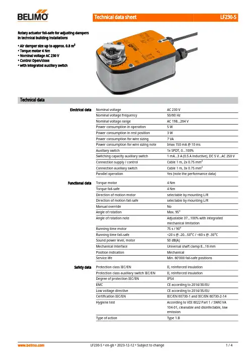
LF230-SRotary actuator fail-safe for adjusting dampersin technical building installations• Air damper size up to approx. 0.8 m²• Torque motor 4 Nm• Nominal voltage AC 230 V• Control Open/close• with integrated auxiliary switchTechnical dataElectrical data Nominal voltage AC 230 VNominal voltage frequency50/60 HzNominal voltage range AC 198...264 VPower consumption in operation 5 WPower consumption in rest position 3 WPower consumption for wire sizing7 VAPower consumption for wire sizing note Imax 150 mA @ 10 msAuxiliary switch1x SPDT, 0...100%Switching capacity auxiliary switch 1 mA...3 A (0.5 A inductive), DC 5 V...AC 250 VConnection supply / control Cable 1 m, 2x 0.75 mm²Connection auxiliary switch Cable 1 m, 3x 0.75 mm²Parallel operation Yes (note the performance data)Functional data Torque motor4 NmTorque fail-safe4 NmDirection of motion motor selectable by mounting L/RDirection of motion fail-safe selectable by mounting L/RManual override NoAngle of rotation Max. 95°Angle of rotation note Adjustable 37...100% with integratedmechanical limitationRunning time motor75 s / 90°Running time fail-safe<20 s @ -20...50°C / <60 s @ -30°CSound power level, motor50 dB(A)Mechanical interface Universal shaft clamp 8...16 mmPosition indication MechanicalService life Min. 60'000 fail-safe positionsSafety data Protection class IEC/EN II, reinforced insulationProtection class auxiliary switch IEC/EN II, reinforced insulationDegree of protection IEC/EN IP54EMC CE according to 2014/30/EULow voltage directive CE according to 2014/35/EUCertification IEC/EN IEC/EN 60730-1 and IEC/EN 60730-2-14Hygiene test According to VDI 6022 Part 1 / SWKI VA104-01, cleanable and disinfectable, lowemissionType of action Type 1.BSafety dataRated impulse voltage supply / control 4 kV Rated impulse voltage auxiliary switch 4 kV Pollution degree 3Ambient humidity Max. 95% RH, non-condensing Ambient temperature -30...50°C [-22...122°F]Storage temperature -40...80°C [-40...176°F]Servicingmaintenance-free WeightWeight 1.7 kg••••••••Safety notesThis device has been designed for use in stationary heating, ventilation and air-conditioning systems and must not be used outside the specified field of application, especially in aircraft or in any other airborne means of transport.Outdoor application: only possible in case that no (sea) water, snow, ice, insolation or aggressive gases interfere directly with the device and that it is ensured that the ambient conditions remain within the thresholds according to the data sheet at any time.Caution: Power supply voltage!Only authorised specialists may carry out installation. All applicable legal or institutional installation regulations must be complied with during installation.The device may only be opened at the manufacturer's site. It does not contain any parts that can be replaced or repaired by the user.Cables must not be removed from the device.To calculate the torque required, the specifications supplied by the damper manufacturers concerning the cross-section and the design, as well as the installation situation and the ventilation conditions must be observed.The device contains electrical and electronic components and must not be disposed of as household refuse. All locally valid regulations and requirements must be observed.Product featuresOperating modeThe actuator moves the damper to the operating position at the same time as tensioning the return spring. The damper is turned back to the safety position by spring energy when the supply voltage is interrupted.Simple direct mounting Simple direct mounting on the damper shaft with a universal shaft clamp, supplied with an anti-rotation device to prevent the actuator from rotating.Adjustable angle of rotation Adjustable angle of rotation with mechanical end stops.High functional reliabilityThe actuator is overload protected, requires no limit switches and automatically stops when the end stop is reached.Flexible signallingWith adjustable auxiliary switch (0...100%)AccessoriesElectrical accessoriesDescriptionType Auxiliary switch 2x SPDTS2A-F Feedback potentiometer 1 kΩP1000A-F Mechanical accessoriesDescriptionType Shaft extension 170 mm ø10 mm for damper shaft ø6...16 mm AV6-20Shaft clamp reversible, clamping range ø16...20 mm K6-1Ball joint suitable for damper crank arm KH8 / KH10KG10A Ball joint suitable for damper crank arm KH8KG8Damper crank arm Slot width 8.2 mm, clamping range ø10...18 mmKH8Description Type Actuator arm, clamping range ø8...16 mm, Slot width 8.2 mm KH-LF Angle of rotation limiter, with end stop ZDB-LF Form fit adapter 8x8 mm ZF8-LF Mounting kit for linkage operation for flat installation ZG-LF1Mounting kit for linkage operation for side installation Slot width 6.2 mm ZG-LF3Anti-rotation mechanism 180 mm, Multipack 20 pcs.Z-ARS180LWire colours:1 = blue2 = brown S1 = violet S2 = redS3 = whiteElectrical installationCaution: Power supply voltage!Parallel connection of other actuators possible. Observe the performance data. Wiring diagramsAC 230 V, open/closeAuxiliary switchLF230-SDimensionsSpindle lengthMin. 84Min. 20Clamping range。

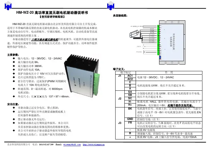
永磁三相无刷电机控制系统说明书上海康丘乐电子电器科技有限公司SHANGHAI KANGQIULE TECHNOLOGY CO.,LTD二0一0年五月康丘乐CTLW系列电动车直流永磁无刷电机控制器使用手册(中小功率部分)适用的产品型号:CTLW4824CTLW4832CTLW4837 CTLW6024CTLW6028CTLW6030 CTLW7214CTLW7220CTLW72241目录第一章概述..................................................3第二章主要特性和规格........................................32.1基本功能..............................................32.2特性..................................................42.3技术参数..............................................52.4型号..................................................5第三章安装方法..............................................63.1安装控制器............................................63.2连线..................................................73.3关于J2第7脚电机相位检测选择信号使用方法........93.4无刷电机控制器总成典型接线图..........................93.5安装后的检查..........................................9第四章维护及附件...........................................104.1清洗.................................................104.2附件(仅对购置控制器总成)...........................11第五章联系方式.............................................122第一章概述本手册对上海康丘乐电子电器科技有限公司(以下简称康丘乐公司)CTLW系列中小功率直流永磁无刷电机控制器产品的特性、安装、使用方法以及维护等方面的知识进行详细地介绍。
R -H B 3-003t i f2 HB3大电流发电机出口断路器开关设备·西门子·2021年R -H B3 -应用HB3大电流发电机出口断路器开关设备·西门子·2021年3目录中压开关设备HB3大电流发电机出口断路器开关设备HB3产品样本·2021/generatorswitchgear该产品样本中所及产品与系统均根据认证管理体系进行生产与销售(符合标准ISO 9001、ISO 14001和 BS OHSAS 18001)。
德国制造4 HB3大电流发电机出口断路器开关设备·西门子·2021年R -H B 3 _ 0 0 0 2 -2 p s d R -H B 3 _ 0 0 0 3 -2 n p s d R -H B 3 -0 0 0 1 -2 p sd 应用概述图 1HB3开关设备示例图 2控制面板示例图 3HB3开关设备示例应用概述概述针对不同发电厂,装设发电机出口断路器开关设备具有许多优点。
发电机装置设出口断路器的优点有:•保护发电机及主变压器•提高供电安全性和稳定性•提高同期操作可靠性•提高保护选择性•遵循电网规程•减少停机时间,提高盈利能力•维护少,维护成本低。
装设 HB3型发电机出口断路器开关设备具有以下优点:可靠的同期操作和发电设备优化•优化发电设备的可用性和安全性•仅在发电机主变压器 (GSUT)的发电机侧进行一次开关操作•双发电机并联运行方式(2台发电机接入 1台主变压器)•抽水蓄能:快速切换发电机和电机运行。
供电安全性高•如果发电机出口断路器因故障电流中断或维护时停用,辅助系统仍可以不间断供应。
保护功能显著提高•发电机电源故障时快速中断,以保护主变压器和辅助变压器•系统电源故障时快速中断,缩小故障范围。
在以下临界条件下切换发电机,如:•大额定电流,大短路电流•大直流分量•高恢复电压上升率(不需要使用真空技术的发电机出口断路器的电容器)•失步切换。
奥伟斯科技为您提供马达控制芯片MC33035DWR2G应用参考设计方案●内容导航:●公司简介●MC33035DWG MC33035DWR2G MC33035P MC33035PG产品规格书●产品图片●主营产品及优势产品简介●公司简介深圳市奥伟斯科技有限公司是一家专注触摸芯片,单片机,电源管理芯片,语音芯片,场效应管,显示驱动芯片,网络接收芯片,运算放大器,红外线接收头及其它半导体产品的研发,代理销售推广的高新技术企业.奥伟斯科技自成立以来一直致力于新半导体产品在国内的推广与销售,年销售额超过壹亿人民币是一家具有综合竞争优势的专业电子元器件代理商.本公司代理推广的一系列优秀触摸芯片及语音芯片,现以大批量应用到智能电子锁、饮水机、电饭煲、LED台灯等控制器为顾客提供最佳解决方案,受到广大客户的一致赞誉。
奥伟斯科技优势行业集中在家用电器和汽车电子领域,包括:智能电子锁、饮水机、抽烟机、空调、洗衣机、冰箱、洗碗机、电饭煲、电磁炉、微波炉、电动自行车、汽车仪表、汽车音响、汽车空调等。
销售网络覆盖华东、华南及华北地区。
奥伟斯科技已为众多世界著名企业提供服务如:美的、小米、云米、长虹、创维、三星、LG、飞利浦、TCL、海尔、美菱、沁园、等众多中国一流品牌电家厂商奥伟斯科技提供专业的智能电子锁触摸解决方案,并提供电子锁整套的芯片配套:低功耗触摸芯片低功耗单片机马达驱动芯片显示驱动芯片刷卡芯片时针芯片存储芯片语音芯片低压MOS管 TVS二极管主要品牌产品:OWEIS-TECH一.电容式触摸芯片ADSEMI触摸芯片代理芯邦科技触控芯片万代科技触摸按键芯片博晶微触摸控制芯片海栎创触摸感应芯片启攀微触摸IC 融和微触摸感应IC 合泰触摸按键IC 通泰触摸芯片二.汽车电子/电源管理/接口芯片/逻辑芯片:IKSEMICON一级代理 ILN2003ADT IK62783DT IL2596 IL2576 ILX485 ILX3485 ILX232 ILX3232 三.功率器件/接收头/光电开关:KODENSHI AUK SMK系列MOS管SMK0260F SMK0460F SMK0760F SMK1260F SMK1820F SMK18T50F四. LED显示驱动芯片:中微爱芯AIP系列 AIP1668 AIP1628 AIP1629 AIP1616天微电子TM系列 TM1628 TM1668TM1621五.电源管理芯片:Power Integrations LNK364PN LNK564PN 芯朋微PN8012 PN8015 AP5054 AP5056 力生美晶源微友达天钰电子FR9886 FR9888六.语音芯片:APLUS巨华电子AP23085 AP23170 AP23341 AP23682 AP89085 AP89170 AP89341 AP89341K AP89682七.运算放大器:3PEAK运算放大器聚洵运算放大器圣邦微运算放大器八.发光二极管:OSRAM欧司朗发光二极管 Lite-On光宝发光二极管 Everlight亿光发光二极管 Kingbright今台发光二极管九. CAN收发器:NXP恩智浦CAN收发器 Microchip微芯CAN收发器十.分销产品线:ONSEMI安森美 TI德州仪器 ADI TOSHIBA东芝 AVAGO安华高十一 MCU单片机ABOV现代单片机MC96F系列 Microchip微芯单片机PIC12F PIC16F PIC18F系列 FUJITSU富仕通单片机MB95F系列 STM单片机STM32F STM32L系列 CKS中科芯单片机CKS32F系列 TI单片机MSP430系列 TMS320F系列 NXP单片机LPC系列MC33035, NCV33035Brushless DC Motor ControllerThe MC33035 is a high performance second generation monolithic brushless DC motor controller containing all of the active functions required to implement a full featured open loop, three or four phase motor control system. This device consists of a rotor position decoder for proper commutation sequencing, temperature compensated reference capable of supplying sensor power, frequency programmable sawtooth oscillator, three open collector top drivers, and three high current totem pole bottom drivers ideally suited for driving power MOSFETs.Also included are protective features consisting of undervoltage lockout, cycle−by−cycle current limiting with a selectable time delayed latched shutdown mode, internal thermal shutdown, and a unique fault output that can be interfaced into microprocessor controlled systems.Typical motor control functions include open loop speed, forward or reverse direction, run enable, and dynamic braking. The MC33035 is designed to operate with electrical sensor phasings of 60︒/300︒ or 120︒/240︒, and can also efficiently control brush DC motors. Features123P SUFFIXPLASTIC PACKAGE CASE 724241DW SUFFIXPLASTIC PACKAGE CASE 751E24(SO−24L)1PIN CONNECTIONS∙ 10 to 30 V Operation ∙ Undervoltage Lockout∙ 6.25 V Reference Capable of Supplying Sensor Power ∙ Fully Accessible Error Amplifier for Closed Loop ServoApplications∙ High Current Drivers Can Control External 3−Phase MOSFET Bridge∙ Cycle−By−Cycle Current Limiting ∙ Pinned−Out Current Sense Reference ∙ Internal Thermal Shutdown∙ Selectable 60︒/300︒ or 120︒/240︒ Sensor Phasings∙ Can Efficiently Control Brush DC Motors with External MOSFET H−Bridge∙ NCV Prefix for Automotive and Other Applications Requiring Site and Control Changes∙ Pb−Free Packages are AvailableTop Drive B T OutputA TFwd/RevS A Sensor S InputsS COutput EnableReference Output Current Sense Noninverting Input Oscillator Error AmpNoninverting Input Error Amp Inverting Input C TBrake 60︒/120︒ Select A B Bottom B B Drive OutputsC B V C V CC Gnd Current Sense Inverting InputFault Output Error Amp Out/PWM Input(Top View)ORDERING INFORMATIONSee detailed ordering and shipping information in the package dimensions section on page 27 of this data sheet.DEVICE MARKING INFORMATIONSee general marking information in the device marking section on page 27 of this data sheet.© Semiconductor Components Industries, LLC, 20041 Publication Order Number:13 1214 11151016 917 818 7 19 620 5 21 422 23 24 BRepresentative Schematic Diagram This device contains 285 active transistors.MAXIMUM RATINGS1. The input common mode voltage or input signal voltage should not be allowed to go negative by more than 0.3 V.2. The compliance voltage must not exceed the range of −0.3 to V ref.3. NCV33035: T low = −40︒C, T high = 125︒C. Guaranteed by design. NCV prefix is for automotive and other applications requiring site and changecontrol.4. MC33035: T A = −40︒C to +85︒C; NCV33035: T A = −40︒C to +125︒C.5. Maximum package power dissipation limits must be observed.φ, E X C E S S P H A S E (D E G R E E S )V s a t , O U T P U T S A T U R A T I O N V O L T A G E (V )∆ , f O S C O S C I L L A T O R F R E Q U E N C Y C H A N G E (%)1004.02.0 10−0 1.010 1001000−R T , TIMING RESISTOR (k Ω) Figure 1. Oscillator Frequency versusTiming Resistor T A , AMBIENT TEMPERATURE (︒C)Figure 2. Oscillator Frequency Changeversus Temperature5648 40 32 24 16 8.0 0 − 8.0 −16 − 24 1.0 k10 k100 k1.0 M40 60 80100 120 140 160180 200 220 240 10 M− 0.8−1.61.60.8 0 01.02.03.04.05.0f, FREQUENCY (Hz)Figure 3. Error Amp Open Loop Gain andPhase versus Frequency I O , OUTPUT LOAD CURRENT (mA)Figure 4. Error Amp Output SaturationVoltage versus Load Current3.053.02.954.53.01.51.0 μs/DIVFigure 5. Error Amp Small−SignalTransient Response 5.0 μs/DIVFigure 6. Error Amp Large−SignalTransient ResponseA V O L , O P E N L O O P V O L T A G E G A I N (dB )f O S C , O S C I L L A T O R F R E Q U E N C Y (k H z )V O , O U T P U T V O L T A G E (V )V O , O U T P U T V O L T A G E (V )V s a t , O U T P U T S A T U R A T I O N V O L T A G E (V )− 4.0 − 8.0 − 12 − 16− 20− 241020304050607.0 6.0 5.0 4.0 3.0 2.01.00 010203040I ref , REFERENCE OUTPUT SOURCE CURRENT (mA)Figure 7. Reference Output Voltage Changeversus Output Source Current V CC , SUPPLY VOLTAGE (V)Figure 8. Reference Output Voltageversus Supply Voltage4020− 2− 41.02.03.04.05.0T A , AMBIENT TEMPERATURE (︒C) Figure 9. Reference Output Voltageversus Temperature PWM I NPUT V OLTAGE (V)Figure 10. Output Duty Cycle versusPWM Input Voltage250200 0.250.2150100 0.150.150 0.050 1.02.03.04.05.0 06.07.08.09.0104.08.0 12 16CURRENT SENSE INPUT VOLTAGE (NORMALIZED TO V th )Figure 11. Bottom Drive Response Time versusCurrent Sense Input Voltage I Sink , SINK CURRENT (mA)Figure 12. Fault Output Saturationversus Sink Current∆V r e f , R E F E R E N C E O U T P U T V O L T A G E C H A N G E (m V )∆V r e f , N O R M A L I Z E D R E F E R E N C E V O L T A G E C H A N G E (m V )t H L , B O T T O M D R I V E R E S P O N S E T I M E (n s ) O U T P U T D U T Y C Y C L E (%)V r e f , R E F E R E N C E O U T P U T V O L T A G E (V )1.21000.80.40 01020 I Sink , S INK C URRENT (mA)3040100 ns/DIVFigure 13. Top Drive Output SaturationVoltage versus Sink CurrentFigure 14. Top Drive Output Waveform1001000 050 ns/DIV50 ns/DIVFigure 15. Bottom Drive Output Waveform Figure 16. Bottom Drive Output Waveform−1.0− 2.02.01.00 02040601614 12 10 8.0 6.0 4.0 2.0 0 805.01015202530I O , OUTPUT LOAD CURRENT (mA)Figure 17. Bottom Drive Output SaturationVoltage versus Load Current V CC , SUPPLY VOLTAGE (V)Figure 18. Power and Bottom Drive SupplyCurrent versus Supply VoltageV s a t , O U T P U T S A T U R A T I O N V O L T A G E (V )O U T P U T V O L T A G E (%) V s a t , O U T P U T S A T U R A T I O N V O L T A G E (V )I C , I C C , P O W E R S U P P L Y C U R R E N T (m A )O U T P U T V O L T A G E (%)O U T P U T V O L T A G E (%)INTRODUCTIONThe MC33035 is one of a series of high performance monolithic DC brushless motor controllers produced by Motorola. It contains all of the functions required to implement a full−featured, open loop, three or four phase motor control system. In addition, the controller can be made to operate DC brush motors. Constructed with Bipolar Analog technology, it offers a high degree of performance and ruggedness in hostile industrial environments. The MC33035 contains a rotor position decoder for proper commutation sequencing, a temperature compensated reference capable of supplying a sensor power, a frequency programmable sawtooth oscillator, a fully accessible error amplifier, a pulse width modulator comparator, three open collector top drive outputs, and three high current totem pole bottom driver outputs ideally suited for driving power MOSFETs.Included in the MC33035 are protective features consisting of undervoltage lockout, cycle−by−cycle current limiting with a selectable time delayed latched shutdown mode, internal thermal shutdown, and a unique fault output that can easily be interfaced to a microprocessor controller.Typical motor control functions include open loop speed control, forward or reverse rotation, run enable, and dynamic braking. In addition, the MC33035 has a 60︒/120︒select pin which configures the rotor position decoder for either 60︒ or 120︒ sensor electrical phasing inputs. FUNCTIONAL DESCRIPTIONA representative internal block diagram is shown in Figure 19 with various applications shown in Figures 36, 38, 39, 43, 45, and 46. A discussion of the features and function of each of the internal blocks given below is referenced to Figures 19 and 36.Rotor Position DecoderAn internal rotor position decoder monitors the three sensor inputs (Pins 4, 5, 6) to provide the proper sequencing of the top and bottom drive outputs. The sensor inputs are designed to interface directly with open collector type Hall Effect switches or opto slotted couplers. Internal pull−up resistors are included to minimize the required number of external components. The inputs are TTL compatible, with their thresholds typically at 2.2 V. The MC33035 series is designed to control three phase motors and operate with four of the most common conventions of sensor phasing. A 60︒/120︒Select (Pin 22) is conveniently provided and affords the MC33035 to configure itself to control motors having either 60︒, 120︒, 240︒or 300︒electrical sensor phasing. With three sensor inputs there are eight possible input code combinations, six of which are valid rotor positions. The remaining two codes are invalid and are usually caused by an open or shorted sensor line. With six valid input codes, the decoder can resolve the motor rotor position to within a window of 60 electrical degrees.The Forward/Reverse input (Pin 3) is used to change the direction of motor rotation by reversing the voltage across the stator winding. When the input changes state, from high to low with a given sensor input code (for example 100), the enabled top and bottom drive outputs with the same alpha designation are exchanged (A T to A B, B T to B B, C T to C B). In effect, the commutation sequence is reversed and the motor changes directional rotation.Motor on/off control is accomplished by the Output Enable (Pin 7). When left disconnected, an internal 25 μA current source enables sequencing of the top and bottom drive outputs. When grounded, the top drive outputs turn off and the bottom drives are forced low, causing the motor to coast and the Fault output to activate.Dynamic motor braking allows an additional margin of safety to be designed into the final product. Braking is accomplished by placing the Brake Input (Pin 23) in a high state. This causes the top drive outputs to turn off and the bottom drives to turn on, shorting the motor−generated back EMF. The brake input has unconditional priority over all other inputs. The internal 40 kΩpull−up resistor simplifies interfacing with the system safety−switch by insuring brake activation if opened or disconnected. The commutation logic truth table is shown in Figure 20. A four input NOR gate is used to monitor the brake input and the inputs to the three top drive output transistors. Its purpose is to disable braking until the top drive outputs attain a high state. This helps to prevent simultaneous conduction of the the top and bottom power switches. In half wave motor drive applications, the top drive outputs are not required and are normally left disconnected. Under these conditions braking will still be accomplished since the NOR gate senses the base voltage to the top drive output transistors.Error AmplifierA high performance, fully compensated error amplifier with access to both inputs and output (Pins 11, 12, 13) is provided to facilitate the implementation of closed loop motor speed control. The amplifier features a typical DC voltage gain of 80 dB, 0.6 MHz gain bandwidth, and a wide input common mode voltage range that extends from ground to V ref. In most open loop speed control applications, the amplifier is configured as a unity gain voltage follower with the noninverting input connected to the speed set voltage source. Additional configurations are shown in Figures 31 through 35.OscillatorThe frequency of the internal ramp oscillator is programmed by the values selected for timing components R T and C T. Capacitor C T is charged from the Reference Output (Pin 8) through resistor R T and discharged by an internal discharge transistor. The ramp peak and valley voltages are typically 4.1 V and 1.5 V respectively. To provide a good compromise between audible noise and output switching efficiency, an oscillator frequency in the range of 20 to 30 kHz is recommended. Refer to Figure 1 for component selection.S A45 Sensor S BInputs 6S C3 Forward/Reverse60︒/120︒S elect22Output Enable 720 k20 k40 k25 μA20 k40 kRotorPositionDecoderV M14Fault Output2A T1 TopDriveB T Outputs24C TV in17V CC18V CUndervoltageLockout ReferenceReference Output 8Noninv. Input 11Faster 12 R T 13RegulatorError AmpPWM9.1 V4.5 VThermalShutdownLatch21A B20 BottomB B DriveOutputsError A mp Out R 19 PWM Input Q C BS10 Oscillator LatchC TSQ 40 kR9 Current Sense Input Sink Only= Positive TrueLogic WithHysteresis16 Gnd100 mV23Brake Input15 Current SenseReference InputFigure 19. Representative Block DiagramNOTES: 1. V = Any one of six valid sensor or drive combinations X = Don’t care.2. The digital inputs (Pins 3, 4, 5, 6, 7, 22, 23) are all TTL compatible. The current sense input (Pin 9) has a 100 mV threshold with respect to Pin 15.A logic 0 for this input is defined as < 85 mV, and a logic 1 is > 115 mV.3. The fault and top drive outputs are open collector design and active in the low (0) state.4. With 60︒/120︒select (Pin 22) in the high (1) state, configuration is for 60︒sensor electrical phasing inputs. With Pin 22 in low (0) state, configurationis for 120︒sensor electrical phasing inputs.5. Valid 60︒or 120︒sensor combinations for corresponding valid top and bottom drive outputs.6. Invalid sensor inputs with brake = 0; All top and bottom drives off, Fault low.7. Invalid sensor inputs with brake = 1; All top drives off, all bottom drives on, Fault low.8. Valid 60︒or 120︒sensor inputs with brake = 1; All top drives off, all bottom drives on, Fault high.9. Valid sensor inputs with brake = 1 and enable = 0; All top drives off, all bottom drives on, Fault low.10. Valid sensor inputs with brake = 0 and enable = 0; All top and bottom drives off, Fault l ow.11. All bottom drives off, Fault low.Figure 20. Three Phase, Six Step Commutation Truth Table (Note 1)Pulse Width ModulatorThe use of pulse width modulation provides an energy efficient method of controlling the motor speed by varying the average voltage applied to each stator winding during the commutation sequence. As C T discharges, the oscillator sets both latches, allowing conduction of the top and bottom drive outputs. The PWM comparator resets the upper latch, terminating the bottom drive output conduction when the positive−going ramp of C T becomes greater than the error amplifier output. The pulse width modulator timing diagram is shown in Figure 21. Pulse width modulation for speed control appears only at the bottom drive outputs.Current Limit sensing an over current condition, immediately turning off the switch and holding it off for the remaining duration of oscillator ramp−up period. The stator current is converted to a voltage by inserting a ground−referenced sense resistor R S (Figure 36) in series with the three bottom switch transistors (Q4, Q5, Q6). The voltage developed across the sense resistor is monitored by the Current Sense Input (Pins 9 and 15), and compared to the internal 100 mV reference. The current sense comparator inputs have an input common mode range of approximately 3.0 V. If the 100 mV current sense threshold is exceeded, the comparator resets the lower sense latch and terminates output switch conduction. The value for the current sense resistor is:Continuous operation of a motor that is severely over−loaded results in overheating and eventual failure.R S =I0.1stator(max)This destructive condition can best be prevented with the use of cycle−by−cycle current limiting. That is, each on−cycle is treated as a separate event. Cycle−by−cycle current limiting is accomplished by monitoring the stator current build−up each time an output switch conducts, and upon The Fault output activates during an over current condition. The dual−latch PWM configuration ensures that only one single output conduction pulse occurs during any given oscillator cycle, whether terminated by the output of the error amp or the current limit comparator.Capacitor C TError A mpOut/PWMInputCurrentSense InputLatch “Set"InputsTop D riveOutputsBottom DriveOutputsFault OutputFigure 21. Pulse Width Modulator Timing Diagram Reference Undervoltage LockoutA triple Undervoltage Lockout has been incorporated to prevent damage to the IC and the external power switch transistors. Under low power supply conditions, it guarantees that the IC and sensors are fully functional, and that there is sufficient bottom drive output voltage. The positive power supplies to the IC (V CC) and the bottom drives (V C) are each monitored by separate comparators that have their thresholds at 9.1 V. This level ensures sufficient gate drive necessary to attain low R DS(on) when driving standard power MOSFET devices. When directly powering the Hall sensors from the reference, improper sensor operation can result if the reference output voltage falls below 4.5 V. A third comparator is used to detect this condition. If one or more of the comparators detects an undervoltage condition, the Fault Output is activated, the top drives are turned off and the bottom drive outputs are held in a low state. Each of the comparators contain hysteresis to prevent oscillations when crossing their respective thresholds.The on−chip 6.25 V regulator (Pin 8) provides charging current for the oscillator timing capacitor, a reference for the error amplifier, and can supply 20 mA of current suitable for directly powering sensors in low voltage applications. In higher voltage applications, it may become necessary to transfer the power dissipated by the regulator off the IC. This is easily accomplished with the addition of an external pass transistor as shown in Figure 22. A 6.25 V reference level was chosen to allow implementation of the simpler NPN circuit, where V ref − V BE exceeds the minimum voltage required by Hall Effect sensors over temperature. With proper transistor selection and adequate heatsinking, up to one amp of load current can be obtained. Fault OutputThe open collector Fault Output (Pin 14) was designed to provide diagnostic information in the event of a system malfunction. It has a sink current capability of 16 mA and can directly drive a light emitting diode for visual indication. Additionally, it is easily interfaced with TTL/CMOS logic for use in a microprocessor controlled system. The Fault Output is active low when one or more of the following conditions occur:1)Invalid Sensor Input code2)Output Enable at logic [0]3)Current Sense Input greater than 100 mVV in1718REF UVLO 4)Undervoltage Lockout, activation of one or more ofthe comparators5)Thermal Shutdown, maximum junction temperaturebeing exceededThis unique output can also be used to distinguish betweenMPS 8 U01ATo motor start−up or sustained operation in an overloaded condition. With the addition of an RC network between the Fault Output and the enable input, it is possible to create aV in SensorPower5.6 V39ControlCircuitry6.25 V1718UVLOtime−delayed latched shutdown for overcurrent. The addedcircuitry shown in Figure 23 makes easy starting of motorsystems which have high inertial loads by providingadditional starting torque, while still preserving overcurrentprotection. This task is accomplished by setting the currentlimit to a higher than nominal value for a predetermined time.MPSU51A0.1 8REF During an excessively long overcurrent condition, capacitorC DLY will charge, causing the enable input to cross itsthreshold to a low state. A latch is then formed by the positiveTo Control Circuitryand Sensor Power6.25 VThe NPN circuit is recommended for powering Hall or opto sensors, where the output voltage temperature coefficient is not critical. The PNP circuit is slightly more complex, but is also more accurate over temperature. Neither circuit has current limiting.Figure 22. Reference Output Buffers feedback loop from the Fault Output to the Output Enable. Once set, by the Current Sense Input, it can only be reset by shorting C DLY or cycling the power supplies.(Drive OutputsThe three top drive outputs (Pins 1, 2, 24) are open collector NPN transistors capable of sinking 50 mA with a minimum breakdown of 30 V. Interfacing into higher voltage applications is easily accomplished with the circuits shown in Figures 24 and 25.The three totem pole bottom drive outputs (Pins 19, 20, 21) are particularly suited for direct drive of N−Channel MOSFETs or NPN bipolar transistors (Figures 26, 27, 28 and 29). Each output is capable of sourcing and sinking up to 100 mA. Power for the bottom drives is supplied from V C (Pin 18). This separate supply input allows the designer added flexibility in tailoring the drive voltage, independent of V CC . A zener clamp should be connected to this input when driving power MOSFETs in systems where V CC is greater than 20 V so as to prevent rupture of the MOSFET gates.The control circuitry ground (Pin 16) and current sense inverting input (Pin 15) must return on separate paths to the central input source ground.Thermal ShutdownInternal thermal shutdown circuitry is provided to protect the IC in the event the maximum junction temperature is exceeded. When activated, typically at 170 C, the IC acts as though the Output Enable was grounded.t DLY = R DLY C DLY InV ref – (I IL enable R DLY )V th enable – (I IL enable R DLY )(6.25 – (20 x 10–6 R DLY ))Transistor Q 1 is a common base stage used to level shift from V CC to the = R DLY C DLY In 1.4 – (20 x 10–6 RDLY )high motor voltage, V M . The collector diode is required if V CC is present while V M is low.Figure 23. Timed Delayed LatchedOver Current Shutdown Figure 24. High Voltage Interface withNPN Power Transistors)The addition of the RC filter will eliminate current−limit instability caused by the leading edge spike on the current waveform. Resistor R S should be a low in- ductance type.Figure 25. High Voltage Interface withN−Channel Power MOSFETsFigure 26. Current Waveform Spike SuppressionI B+ 0 t−Base Charge RemovalSeries gate resistor R g will dampen any high frequency oscillations caused by the MOSFET input capacitance and any series wiring induction in the gate−source circuit. Diode D is required if the negative current into the Bot- tom Drive Outputs exceeds 50 mA.The totem−pole output can furnish negative base current for enhanced tran- sistor turn−off, with the addition of capacitor C.Figure 27. MOSFET Drive PrecautionsFigure 28. Bipolar Transistor Drive21D SENSEFETG S MK20199 15R SPower Ground:To Input Source ReturnR S · I pk · R DS(on)100 mVV Pin 9 =r DM(on) + R S16 GndIf: SENSEFET = MPT10N10M R S = 200 Ω, 1/4 W Then : V Pin 9 ≈ 0.75 I pkControl Circuitry Ground (Pin 16) and Current Sense Inverting Input (Pin 15) must return on separate paths to the Central Input Source Ground.Virtually lossless current sensing can be achieved with the implementation of SENSEFET power switches.This circuit generates V Boost for Figure 25.Figure 29. Current Sensing Power MOSFETs Figure 30. High Voltage Boost SupplyV AV BV = V (R 3 + R 4) R 2(R 4 V )Resistor R 1 with capacitor C sets the acceleration time constant while R 2 controls the deceleration. The values of R 1 and R 2 should be at least ten Pin 13 A R 1 + R 2 3 —R 3 Btimes greater than the speed set potentiometer to minimize time constant variations with different speed settings.Figure 31. Differential Input Speed Controller Figure 32. Controlled Acceleration/DecelerationR B o o s t V o l t a g e (V )S N 74L S 145 ( )5.0 V16 11V CC Q 910 Q 8166 k 145 k100 k 8 REFQ 9 126 k 12 P313 BCD 14 P2 Inputs P1 7Q 6 7 Q 5 6 Q 4 5 108 k92.3 k 77.6 k 7 25 μA11EA1215 P0 Q 3 4 Q2 363.6 k 51.3 k 13 PWMQ 1Gnd Q 082 40.4 k 1The SN74LS145 is an open collector BCD to One of Ten decoder. When con- nected as shown, input codes 0000 through 1001 steps the PWM in incre- ments of approximately 10% from 0 to 90% on−time. Input codes 1010 through 1111 will produce 100% on−time or full motor speed.The rotor position sensors can be used as a tachometer. By differentiating the positive−going edges and then integrating them over time, a voltage proportional to speed can be generated. The error amp compares this volt- age to that of the speed set to control the PWM.Figure 33. Digital Speed Controller Figure 34. Closed Loop Speed ControlVR 3 + R 4RR4Pi n 3 =V ref V V ref 1 23 3 8 B =R 5 + 1 R 6R 1T7 R 511 R 2 312 25 μAEAR 3 >> R 5 ǁ R 66R 413PWM This circuit can control the speed of a cooling fan proportional to the differencebetween the sensor and set temperatures. The control loop is closed as the forced air cools the NTC thermistor. For controlled heating applications, ex- change the positions of R 1 and R 2.Figure 35. Closed Loop Temperature ControlR R。
控制电机MY3000■概要控制电机MY3000是电机的一种。
该电机通过与联动装置组合可对控制阀和风门进行操作。
Array控制方法如下:①当与一个数字控制器(如WY5111等)组合时,带有内装式公称135Ω反馈电位计的控制电机进行比例控制。
②当与一个电比例控制器(如TY9000、TY991等)组合时,公称135Ω电阻输入型进行比例控制。
③当与一个数字控制器(如WY5111、R15/35/36等)组合时,4~20mADC输入型进行比例控制。
④当与一个数字控制器(如WY5117等)组合时,2~10VDC输入型进行比例控制。
⑤当与一个数字式控制器(如WY7207等)组合时,ON/OFF或浮动型进行浮动控制。
在将该控制电机与控制阀组合的情况下,通过使用阀门联动装置Q455进行安装;在将该控制电机与风门组合的情况下,通过使用风门联动装置Q605进行安装。
■特点(1) 备有丰富的控制输入信号类型。
(2) 功率低,使用寿命长。
(3) 辅助开关的安装简单易行。
(4) 通过联动装置,可驱动各种尺寸的阀门、风门。
AI-6387C安全注意事项使用前请仔细阅读本使用说明书,并在此基础上正确地使用本产品。
阅读后,请务必将使用说明书保管在可随时查阅的地方。
使用上的限制和注意事项本产品用于普通的空调控制。
请勿在有碍人身安全的情况下使用本产品。
另外,当用于洁净室、动物棚舍等对可靠性、控制精度有特别要求的用途时,请咨询本公司的销售人员。
对由于用户使用不当造成的后果,本公司概不负责。
敬请谅解!警 告z更换配线必须在电源切断的状态(本产品电源端子上的接线与电源电路相脱离的状态)下进行。
否则可能导致触电。
注 意z请在规格栏所记载的使用条件(温度、湿度、电压、振动、冲击、安装方向和空气环境等)范围内使用本产品。
否则,将会导致火灾或设备故障。
z请在规格栏所定的额定范围内使用本产品。
否则,将导致设备故障。
z请在寿命范围内使用本产品。
在计装时,请注意不要让本产品工作次数过多。
无BX 系列相 关 情 报B-7BXFBL Ⅱ使用须知刷直流电动机新 产 品技术资料 ……………………………………………G-1其他相关介绍 ………………………………………H-1无刷直流电动机无刷直流电动机组合产品BX系列高性能·高功能的无刷直流电动机组合产品。
备有30W~400W高输出的种类。
在基本型的高性能之速度控制下,加上系统升级套件的组合之后,即可使用转矩控制功能、定位控制模式等。
■特征●广泛的速度控制范围·均匀转矩在30r/min~3000r/min广泛的可变速度控制范围内、发挥低速至高速的均匀转矩。
通过更高的起动转矩时可在起动、停止时,使用较大的转矩。
●卓越的速度稳定性其速度变动率为±0.05%(对负载)时,实现了高精度的速度控制。
此外,可在中高速时、大幅减低运行的不均匀现象。
●上下驱动时可控制速度使用带电磁制动电动机进行上下驱动(下降运行)时,仍可稳定的控制速度。
也可以通过驱动器进行自动控制电磁制动。
请注意∶ 上下驱动时,产生再生能量。
请务必使用另售的再生器。
●系统升级套件可提升性能加上另售的系统升级套件并经数字设定后,可大幅提高速度控制的功能与特性。
·扩大速度控制范围 3~3000r/min·改善速度变动率 对温度∶±0.05%(基本型∶±0.5%)·最多可设定8段速度数据(基本型∶2段)〈系统升级套件〉数据设定器OPX-1A●转矩限制功能使用系统升级套件,即可使用转矩限制功能。
对应用途或使用状况,转矩限制功能可控制电动机输出转矩。
●定位控制模式只需以系统升级套件设定数据,即可控制定位。
分辨率达0.72˚(500脉冲/1转)节,最多可设定6点的定位数据,其中可设定至2点为连续运行用。
此外,也可以设定机械原点返回、电原点返回运行。
■规格·CE标志●各类安全规格乃以电动机单体品名或驱动器单体品名申请取得认证。