
PCB-BITE
- 格式:xls
- 大小:12.00 KB
- 文档页数:1

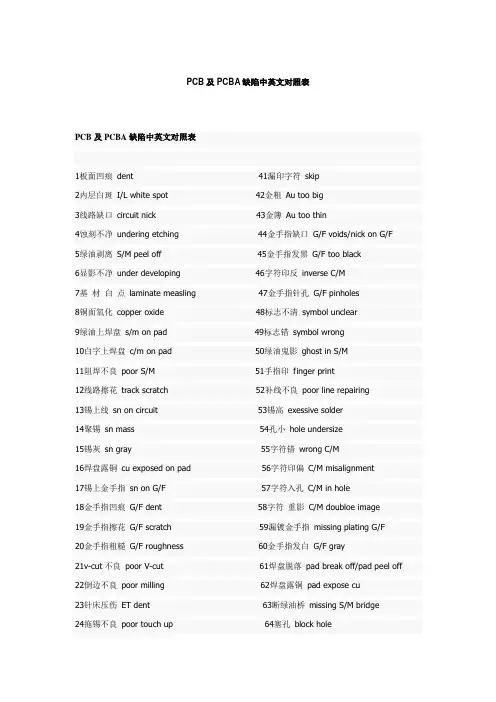
PCB及PCBA缺陷中英文对照表PCB及PCBA缺陷中英文对照表1板面凹痕dent 41漏印字符skip2内层白斑I/L white spot 42金粗Au too big3线路缺口circuit nick 43金簿Au too thin4蚀刻不净undering etching 44金手指缺口G/F voids/nick on G/F 5绿油剥离S/M peel off 45金手指发黑G/F too black6显影不净under developing 46字符印反inverse C/M7基材白点laminate measling 47金手指针孔G/F pinholes8铜面氧化copper oxide 48标志不清symbol unclear9绿油上焊盘s/m on pad 49标志错symbol wrong10白字上焊盘c/m on pad 50绿油鬼影ghost in S/M11阻焊不良poor S/M 51手指印finger print12线路擦花track scratch 52补线不良poor line repairing13锡上线sn on circuit 53锡高exessive solder14聚锡sn mass 54孔小hole undersize15锡灰sn gray 55字符错wrong C/M16焊盘露铜cu exposed on pad 56字符印偏C/M misalignment17锡上金手指sn on G/F 57字符入孔C/M in hole18金手指凹痕G/F dent 58字符重影C/M doubloe image19金手指擦花G/F scratch 59漏镀金手指missing plating G/F20金手指粗糙G/F roughness 60金手指发白G/F gray21v-cut不良poor V-cut 61焊盘脱落pad break off/pad peel off 22倒边不良poor milling 62焊盘露铜pad expose cu23针床压伤ET dent 63断绿油桥missing S/M bridge24拖锡不良poor touch up 64塞孔block hole25补金不良poor repairing Au 65水迹water print26补油不良poor repairing s/m 66锡珠solder ball27针孔pinhole 67砂孔pitting28胶渍paster stain 68油薄S/M too thin29k孔内毛刺burrs in hole 69聚油excess solder mask 30锡珠入孔solder in hole 70锡粗Sn too thick31露铜expose Cu 71线路上锡Sn overlap scratch 32露镍expose Ni 72绿油下杂物contamination under S/M 33绿油起泡solder mask blister 73焊盘损坏land damage34绿油起皱solder mask winbles 74焊盘翘起lifted land35金手指氧化G/F oxiding 75偏位misregistration36金颜色不良Au discoloration 76漏钻孔missing hole37金面凸起Au surface blister 77焊盘缺口nick on pad 38绿油入孔solder mask in hole 78线路缺口nick on track 39爆板board angle damafe40翘板warp1开路open circuit 46焊盘翘起lifted land2短路short circuit 47漏钻孔missing hole线路狗牙circuit wist 48露布纹weave exposure3线路缺口circuit nick 49钻偏孔hole misregistratiion 4线路凹痕circuit dent 50孔损害hole damage5渗镀plating Bloody 51基材分层delamination6焊盘缺口pad nick 52蚀刻过度over etching7内层白斑I/L white spot 53多孔hole too much8黑化不良poor B.O 54残铜remain Cu9爆板measling 55孔内露基材laminate exposure in hole10粉红圈pinking ring 56焊盘脱落pad break off 11层压起泡press blister 57焊盘凹痕pad dent12错位misregistation 58焊盘凸起pad bulge13偏位shift 59焊盘损坏pad damaged14孔内无铜no Cu on Pth 60焊盘缺口pad nick15孔内毛刺hole burrs 61焊盘露铜pad expose Cu 16NPTH有铜Cu on NPTH 30修理不良poor repairing17铜面露基材exposed laminate 31铜薄copper too thin18铜面凹痕dent on Cu surface 32内层擦花I/L scratch19胶渍gum residue 33内层偏位I/L misregistation20夹膜D/F nip 34内层杂物I/L inclusions21蚀刻不尽under etching 35掉膜film off22线幼line too thin 36干膜碎D/F meaking23孔大hole oversize 37退锡不尽poor Sn stripping 24孔小hole undersize 38间隙小space too marrow 25偏孔hole misregistration 39板薄board too thin26铜面瘤粒Cu nodule 40板厚board too thickness27显影不尽under developing 41针孔pinhole28铜面刮伤scratch on Cu surface 42崩孔breakout29塞孔hole plugged 43侧蚀undrcut45亚色dull colour 44镀层粗糙plating layer roughness PCB及PCBA常用度量衡单位换算所属目录:FASTPCBA靖邦公司资料发布时间:2009-01-01 1英尺=12英寸1英寸inch=1000密尔mil1mil=25.4um1mil=1000uin mil密耳有时也成英丝1um=40uin(有些公司称微英寸为麦,其实是微英寸)1OZ=28.35克/平方英尺=35微米H=18微米4mil/4mil=0.1mm/0.1mm线宽线距1ASD=1安培/平方分米=10.76安培/平方英尺1AM=1安培分钟=60库仑主要用于贵金属电镀如镀金1平方分米=10.76平方英尺1盎司=28.35克,此为英制单位1加仑(英制)=4.5升1加仑美制=3.785升1KHA=1000安小时1安培小时=3600库仑比重波美度=145-145/比重SG.SG.比重(克/立方厘米)=145/(145-波美PCB及PCBA行业专用名词PCB及PCBA行业专用名词BOM(Bill of material) 物料需求單Laminate 基板Copper foil 銅箔Solder mask(s/m) 防焊Bare Board 空板Microetching 微蝕Exposure 曝光Dry Film 干膜Matte side 毛面Rcc(Resin coated copper) 背膠銅箔Final shaping 成型Electrical test(ET) 電測Visual Inspection 外觀檢查Gold Finger(G/F) 金手指Legend 文字Post Cure 后烤Desmear 除膠渣Developing 顯影Pattern Plating 線路電鍍Panel Plating 全板電鍍Puddle Effect 水坑效應Oxide Coating 黑氧化Routing Bit 銑刀Tolerance 公差Post Treatment 后處理Adhesion 附著力Stripping 去膜Baking 烘烤AQL(acceptable quality level) 品質允收水準Optical Target 光學靶點Lay up 疊合Chromation 鉻化處理Undercut 側蝕Microvia 微孔Annular Ring 孔環Burr 毛頭Entek 有機保焊處理Conformal Mask 銅窗Drum Side 光面Diazo Film 偶氮棕片Cut Lamination 下料Sheets Cutting 裁板Inner Layer Drilling 內層鑽孔Outter Layer Drilling 一次孔2nd Drilling 二次孔PCB及PCBA专用名词Laser Drilling 雷射鉆孔Blind&Burried Hole Drilling 盲(埋)孔鉆孔screen printing 網版印刷silk screen 絲網印刷scum 透明殘膜skip printing 跳印漏印squeege 刮刀type 种類abietic acid 松脂酸air knife 風刀bridging 搭橋橋接flux 助焊劑product process 制程pre-process 制前solder bridge 錫橋soler bump 錫突solder plug 錫塞immersion gold 浸金(化金)thin core 薄基板twist 板翘, 板扭warp ,warpage 板彎weave eposure 織紋顯露wicking 燈蕊效應yield 良品abrasion resistance 耐磨性absorption 吸收accelerated test 加速實驗acceleration 速化反應accelerator 加速剂batch 批cold solder joint 冷焊點component side 零件面double side 雙面double side board 雙面板fiducial mark 基準記號finished board 成品板lot size 批量rack 掛架register mark 對準用標記solder side 錫鉛面thickness 厚度warehouse 仓库wet process 濕制程Beveling 斜邊chamfer 道角dimension 尺寸Fixture 治具interconnection 互相連通line space 線距line width 線寬misregistration 對不准mouse bite 蝕刻缺口nick 缺口master drawing 主圖print and etch board 印刷後及蝕刻後板crease 皺褶dent 凹陷glass fiber 玻璃纖維布pin hole 針孔pit 凹點target hole 靶孔PCBA及PCB专用名词(二)PCBA及PCB专用名词(二)Black Oxide Removal 黑化還原Plug Hole 塞孔Ink Print&precure 印刷及預烤Scrub 表面處理Spray Coating 靜電噴涂Printing of Legend 文字印刷Pumice ( Wet Blasting) 噴砂Immersion Ni/Au(Electoless Ni/Au) 浸鎳金Hot Air Solder Leveling 噴錫N/C routing 撈型Beveling of G/F 金手指斜边Cleanning&Baking 清洗及烘烤Fixture Testing 治具測試original A/W 客戶原稿working A/W 工作片working master 工作母片carlson pin 定位梢component hole(>30mil) 零件孔drill facet 鑽尖切削面drill pointer 鑽尖重磨機drilled blank board 已鑽孔的裸板hole diameter 孔徑hole location 孔位hole number 孔數lay back 刃角磨損margin 鑽頭刃帶open circuits 斷路runout 偏轉slot 開槽spindle 鑽軸tooling hole 工具孔stacking structure 疊板結構blow hole, void in PTH hole 吹孔孔破deburring 去毛頭electroless-deposition 無電鍍化etchback 回蝕air inclusion 氣泡chase 網框fabric 網布liquid 液態\狀mealing 泡點trim line 裁切線v-cut v型切槽golden board 標準板back lighting 背光crack 裂痕crazing 白斑dimension stability 尺寸安全性failure 故障fault 缺陷瑕疵gap 鑽尖分開gel time 膠化時間haloing 白邊白圈hardener 硬化劑hole counter 數孔機hook 外弧insulation resistance 絕緣阻抗ionizable(ionic) contaminants 離子性污染land 焊墊microsectioning 微切片法negative etchback 反回蝕overlap 鑽尖重曡peel strength 抗撕強度pink ring 粉紅圈REJ(reject) 拒收退貨release agent(sheets) 脫膜劑resin content 膠含量resin flow 膠流量resin recession 樹脂下限resin smear 膠渣rework 重工specification(spec.) 規範innerlayer&outlayer 內外層gold plating 鍍金QC(quality control) 品管back up 墊板blister 起泡局部分层caul plate 隔板, 钢板open circuits 断路sampling size 抽樣數edge spacing 板邊空地ground plane 接地層laminator 壓膜機M/T 磁帶disk 磁片。
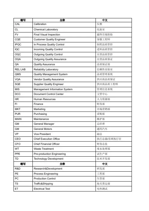

TWN4 PALON COMPACT COMPACT OEM RFID READER/WRITER FOR LF, HF, NFC, BLE, WITH EXTENDED INTERFACESTWN4 Palon Compact is a versatile OEM PCB for integration into third-party products and devices. It supports enhanced interfaces, especially RS-485. The new compact PCB module inherits all advantages and integrated tool support of the ELATEC TWN4 family. Although it is a general-purpose device, it is optimized for time attendance and access control.TWN4 Palon is a multi-technology reader/writer family supporting almost all 125 kHz/134.2 kHz and 13.56 MHz contactless technologies, including NFC. RS-485, RS-232, Wiegand, Clock/Data and USB are standard interfaces. Optionally, OSDP protocol is supported. On-board antennas for HF and LF allow excellent contactless performance. An integrated Bluetooth Low Energy (BLE) module supports a broad range of mobile ID and authentication solutions as well.Special features:Optimized PCB design for OEM integrationOnboard LF and HF antennasOne onboard SAM socket (Secure Access Module)Interfaces: RS-485, RS-232 and TTL (Wiegand, Clock/Data). OSDP protocol optionallyMicro USB portSupports quick (re)configuration over network and over wireless interface with TWN4 CONFIG CardDirect chip-commands supportIntegrated BLE module 2.4 GHz for data communication and authentication, Bluetooth v4.2, upgradableFirmware update in the field possiblePowerful SDK for writing apps which are executed directly on the readerOnboard 18 kB flash storage, e.g. for storing user accessible non-volatile dataSupports quick centralized (re)configuration over network and over wireless interface with TWN4 CONFIG CardTWN4 Upgrade Card for P and PI options available on request3D construction data (STEP) available on request7)On request 8)Without encryptionDrawing / rear view PCB Assignment of DIP switch relates to version with RS-485. Firmware may change the assignment of the DIP switch. Pleaserefer to the TWN4 Palon manual. For RS-232, Wiegand, Clock/Data the DIP switch is not used.(Dimensions mm) Drawing / front view PCB side viewELATEC GmbH • Zeppelinstr. 1 • 82178 Puchheim • GermanyP +49 89 552 9961 0 • F +49 89 552 9961 129 • E-Mail:********************ELATEC reserves the right to change any information or data in this document without prior notice. ELATEC declines all responsibility for the use of this product with any other specification but the one mentioned above. Any additional requirement for a specific customer application has to be validated by the customer himself at his own responsibility. Where application information is given, it is only advisory and does not form part of the specification. Disclaimer: All names used in this doc ument are registered trademarks of their respective owners.。

PCB端子1. 简介PCB端子是电子设备中常用的连接部件,用于连接电路板和外部电路或设备。
它们通过插针或插座的形式提供电信号或电源传输。
PCB端子广泛应用于各种电子设备中,包括电脑、手机、家电等。
2. PCB端子的类型PCB端子的种类繁多,常见的类型有:2.1 螺钉端子螺钉端子是一种常用且可靠的连接方式,它通过螺丝将导线固定在端子上。
当需要更换线缆时,只需要拧松螺丝即可。
这种端子适用于大功率和高电流的连接。
2.2 弹簧式端子弹簧式端子使用弹簧夹紧导线,简化了连接过程。
它们通常用于低功率的连接,如传感器和模块之间的连接。
弹簧式端子的优点包括插拔次数多、连接稳定可靠、可防止接触不良。
2.3 压接端子压接端子是通过压接工具将导线压接在接触片上,实现电气连接。
这种端子通常用于较小功率和较低电流的连接,如电子元器件连接。
2.4 插座式端子插座式端子通常用于连接电子设备和外部电路,提供方便的插拔功能。
常见的插座式端子有D型插座、USB插座等。
它们广泛应用于计算机、手机和家用电器等领域。
2.5 可编程器连接端子可编程器连接端子是用于连接可编程器与目标板的接口,它们用于编程和测试电路板。
这些端子常用于生产线上的测试和编程步骤。
3. PCB端子的选型考虑因素在选择合适的PCB端子时,需要考虑以下因素:3.1 电流和功率需求根据电流和功率需求,选择适当的端子类型和规格。
对于大功率和高电流的连接,螺钉端子是一个理想的选择。
对于低功率连接,弹簧式、压接式或插座式端子可以满足需求。
3.2 空间限制PCB板上的空间有限,因此需考虑端子的尺寸和布局。
对于紧凑的布局,可能需要选择小型的端子类型或表面贴装端子。
3.3 环境要求考虑端子使用的环境条件,如温度、湿度、振动等因素。
对于恶劣环境下的应用,需选择耐腐蚀、耐高温或防水的端子。
3.4 插拔次数如果需要频繁插拔连接,弹簧式或插座式端子是更好的选择,因为它们具有较高的插拔次数和较低的接触阻抗。