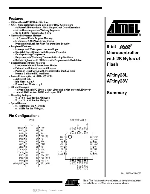
ATTINY24A-SSU中文资料FeaturesHigh Performance, Low Power AVR? 8-Bit MicrocontrollerAdvanced RISC Architecture–120 Powerful Instructions –Most Single Clock Cycle Execution–32 x 8 General Purpose Working Registers–Fully Static OperationHigh Endurance, Non-Volatile Memory Segments–2K/4K Bytes of In-System, Self-Programmable Flash Program MemoryEndurance: 10,000 Write/Erase Cycles–128/256 Bytes of In-System Programmable EEPROMEndurance: 100,000 Write/Erase Cycles–128/256 Bytes of Internal SRAM–Data retention: 20 years at 85°C / 100 years at 25°C–Programming Lock for Self-Programming Flash & EEPROM Data Security ?Peripheral Features–One 8-Bit and One 16-Bit Timer/Counter with Two PWM Channels, Each–10-bit ADC8 Single-Ended Channels12 Differential ADC Channel Pairs with Programmable Gain (1x / 20x)–Programmable Watchdog Timer with Separate On-chip Oscillator–On-Chip Analog Comparator–Universal Serial InterfaceSpecial Microcontroller Features–debugWIRE On-chip Debug System–In-System Programmable via SPI Port–Internal and External Interrupt SourcesPin Change Interrupt on 12 Pins–Low Power Idle, ADC Noise Reduction, Standby and Power-Down Modes –Enhanced Power-on Reset Circuit–Programmable Brown-Out Detection Circuit with Software Disable Function –Internal Calibrated Oscillator–On-Chip Temperature SensorI/O and Packages–Available in 20-Pin QFN/MLF & 14-Pin SOIC and PDIP–Twelve Programmable I/O LinesOperating Voltage:–1.8 – 5.5VSpeed Grade:–0 –********– 5.5V–0 –*********– 5.5V–0 –*********– 5.5VIndustrial Temperature Range: -40°C to +85°CLow Power Consumption–Active Mode:210 μA at 1.8V and 1MHz–Idle Mode:33 μA at 1.8V and 1MHz–Power-Down Mode:0.1 μA at 1.8V and 25°C 8-bit Microcontrollerwith 2K/4KBytes In-System ProgrammableATtiny24A (Preliminary)ATtiny44A28183AS–AVR–12/08ATtiny24A/44A1.Pin ConfigurationsFigure 1-1.Pinout of ATtiny24A/44A1.1Pin Descriptions1.1.1VCCSupply voltage.1.1.2GNDGround.1.1.3Port B (PB3...PB0)Port B is a 4-bit bi-directional I/O port with internal pull-up resistors (selected for each bit). The Port B output buffers have symmetrical drive characteristics with both high sink and source RES ET pin, program (‘0’) RSTDISBL fuse. As inputs, Port B pins that are externally pulled low will source current if the pull-up resistors are activated. The Port B pins are tri-stated when a reset condition becomes active, even if the clock is not running.1234567141312111098VCC(PCINT 8/XT AL1/CLKI) PB0(PCINT9/XTAL2) PB1(PCINT11/RE S ET/dW) PB 3(PCINT10/INT0/OC0A/CKOUT) PB2(PCINT7/ICP/OC0B/ADC7) PA7(PCINT6/OC1A/S DA/MO S I/DI/ADC6) PA6GNDPA0 (ADC0/AREF/PCINT0)PA1 (ADC1/AIN0/PCINT1)PA2 (ADC2/AIN1/PCINT2)PA 3 (ADC 3/T0/PCINT 3)PA4 (ADC4/U S CK/S CL/T1/PCINT4)P A5 (ADC5/DO/MI S O/OC1B/PCINT5)PDIP/S OIC12345QFN/MLF15141312112019181716678910NOTEBottom p a d s ho u ld b e s oldered to gro u nd.DNC: Do Not ConnectD N C D N C G N D V C C D N CPA7 (PCINT7/ICP/OC0B/ADC7)PB2 (PCINT10/INT0/OC0A/CKOUT)PB 3 (PCINT11/RE S ET/dW)PB1 (PCINT9/XTAL2)PB0 (PCINT 8/XTAL1/CLKI)P A 5D N C D N C D N C P A 6Pin 16: P A6 (PCINT6/OC1A/S DA/MO S I/DI/ADC6)Pin 20: P A5 (ADC5/DO/MI S O/OC1B/PCINT5)(ADC4/U S CK/S CL/T1/PCINT4) PA4(ADC 3/T0/PCINT 3) PA 3(ADC2/AIN1/PCINT2) PA2(ADC1/AIN0/PCINT1) PA1(ADC0/AREF/PCINT0) PA038183AS–AVR–12/08ATtiny24A/44APort B also serves the functions of various special features of the ATtiny24A/44A as listed in Section 10.2 “Alternate Port Functions” on page 57.Reset input. A low level on this pin for longer than the minimum pulse length will generate a reset, even if the clock is not running and provided the reset pin has not been disabled. The min-imum pulse length is given in Table 20-4 on page 176. Shorter pulses are not guaranteed to generate a reset.The reset pin can also be used as a (weak) I/O pin.1.1.5Port A (PA7...PA0)Port A is a 8-bit bi-directional I/O port with internal pull-up resistors (selected for each bit). The Port A output buffers have symmetrical drive characteristics with both high sink and source capability. As inputs, Port A pins that are externally pulled low will source current if the pull-up resistors are activated. The Port A pins are tri-stated when a reset condition becomes active,even if the clock is not running.Port A has alternate functions as analog inputs for the ADC, analog comparator, timer/counter,SPI and pin change interrupt as described in “Alternate Port Functions” on page 57.48183AS–AVR–12/08ATtiny24A/44A2.OverviewATtiny24A/44A are low-power CMOS 8-bit microcontrollers based on the AVR enhanced RISC architecture. By executing powerful instructions in a single clock cycle, the ATtiny24A/44A achieves throughputs approaching 1 MIPS per MHz allowing thesystem designer to optimize power consumption versus processing speed.Figure 2-1.Block DiagramThe AVR core combines a rich instruction set with 32 general purpose working registers. All 32registers are directly connected to the Arithmetic Logic Unit (ALU), allowing two independent registers to be accessed in one single instruction executed in one clock cycle. The resulting architecture is more code efficient while achieving throughputs up to ten times faster than con-ventional CISC microcontrollers.58183AS–AVR–12/08ATtiny24A/44AThe ATtiny24A/44A provides the following features: 2K/4K byte of In-System Programmable Flash, 128/256 bytes EEPROM, 128/256 bytes SRAM, 12 general purpose I/O lines, 32 general purpose working registers, an 8-bit Timer/Counter with two PWM channels, a 16-bit timer/coun-ter with two PWM channels, Internal and External Interrupts, a 8-channel 10-bit ADC,programmable gain stage (1x, 20x) for 12 differential ADC channel pairs, a programmable Watchdog Timer with internal oscillator, internal calibrated oscillator, and four software select-able power saving modes. Idle mode stops the CPU while allowing the SRAM, Timer/Counter,ADC, Analog Comparator, and Interrupt system to continue functioning. ADC Noise Reduction mode minimizes switching noise during ADC conversions by stopping the CPU and all I/O mod-ules except the ADC. In Power-down mode registers keep their contents and all chip functionsare disbaled until the next interrupt or hardware reset. In Standby mode, the crystal/resonator oscillator is running while the rest of the device is sleeping, allowing very fast start-up combined with low power consumption.The device is manufactured using Atmel’s high density non-volatile memory technology. The on-chip ISP Flash allows the Program memory to be re-programmed in-system through an SPI serial interface, by a conventional non-volatile memory programmer or by an on-chip boot code running on the AVR core.The ATtiny24A/44A AVR is supported with a full suite of program and system development tools including: C Compilers, Macro Assemblers, Program Debugger/Simulators and Evaluation kits.68183AS–AVR–12/08ATtiny24A/44A3.About3.1ResourcesA comprehensive set of drivers, application notes, data sheets and descriptions on development tools are available for download at /doc/fb6038e319e8b8f67c1cb9ea.html/avr.3.2Code ExamplesThis documentation contains simple code examples that briefly show how to use various parts of the device. These code examples assume that the part specific header file is includedbefore compilation. Be aware that not all C compiler vendors include bit definitions in the header files and interrupt handling in C is compiler dependent. Please confirm with the C compiler documen-tation for more details.For I/O Registers located in the extended I/O map, “IN”, “OUT”, “SBIS”, “SBIC”, “CBI”, and “SBI”instructions must be replaced with instructions that allow access to extended I/O. Typically, this means “LDS” and “STS” co mbined with “SBRS”, “SBRC”, “SBR”, and “CBR”. Note that not all AVR devices include an extended I/O map.3.3Data RetentionReliability Qualification results show that the projected data retention failure rate is much less than 1 PPM over 20 years at 85°C or 100 years at 25°C.3.4DisclaimerTypical values contained in this datasheet are based on simulations and characterization of other AVR microcontrollers manufactured on the same process technology. Min and Max values will be available after the device has been characterized.78183AS–AVR–12/08ATtiny24A/44A4.Register SummaryAddressNameBit 7Bit 6Bit 5Bit 4Bit 3Bit 2Bit 1Bit 0Page0x3F (0x5F)SREG I T H S V N Z C Page 80x3E (0x5E)SPH ––––––SP9SP8Page 100x3D (0x5D)SPL SP7SP6SP5SP4SP3SP2SP1SP0Page 100x3C (0x5C)OCR0B Timer/Counter0 – Output Compare Register B Page 830x3B (0x5B)GIMSK –INT0PCIE1PCIE0––––Page 490x3A (0x5A GIFR –INTF0PCIF1PCIF0––––Page 500x39 (0x59)TIMSK0–––––OCIE0B OCIE0A TOIE0Page 830x38 (0x58)TIFR0––––OCF0BOCF0A TOV0Page 830x37 (0x57)SPMCSR ––RSIG CTPB RFLB PGWRTPGERS SPMEN Page 1560x36 (0x56)OCR0A Timer/Counter0 – Output Compare Register A Page 820x35 (0x55)MCUCR BODS PUD SE SM1SM0BODSE ISC01ISC00Pages 35, 49, and 65 0x34 (0x54)MCUSR ––––WDRF BORF EXTRF PORF Page 430x33 (0x53)TCCR0B FOC0A FOC0B ––WGM02CS02CS01CS00Page 810x32 (0x52)TCNT0Timer/Counter0Page 820x31(0x51)OSCCAL CAL7CAL6CAL5CAL4CAL3CAL2CAL1CAL0Page290x30 (0x50)TCCR0A COM0A1COM0A0COM0B1COM0B0–WGM01WGM00Page 780x2F (0x4F)TCCR1A COM1A1COM1A0COM1B1COM1B0–WGM11WGM10Page 1060x2E (0x4E)TCCR1B ICNC1ICES1–WGM13WGM12CS12CS11CS10Page 1080x2D (0x4D)TCNT1H Timer/Counter1 –Counter Register High Byte Page 1100x2C (0x4C)TCNT1L Timer/Counter1 –Counter Register Low Byte Page 1100x2B (0x4B)OCR1AH Timer/Counter1 – Compare Register A High Byte Page 1100x2A (0x4A)OCR1AL Timer/Counter1 – Compare Register A Low Byte Page 1100x29 (0x49)OCR1BH Timer/Counter1 –Compare Register B High Byte Page 1100x28 (0x48)OCR1BL Timer/Counter1 – Compare Register B Low BytePage 1100x27 (0x47)DWDR DWDR[7:0]Page 1510x26 (0x46)CLKPR CLKPCE–––CLKPS3CLKPS2CLKPS1CLKPS0Page 300x25 (0x45)ICR1H Timer/Counter1 - Input CaptureRegister High Byte Page 1110x24 (0x44)ICR1L Timer/Counter1 - Input Capture Register Low BytePage 1110x23 (0x43)GTCCR TSM ––––––PSR10Page 1140x22 (0x42)TCCR1C FOC1A FOC1B ––––––Page 1090x21 (0x41)WDTCSR WDIF WDIE WDP3WDCE WDE WDP2WDP1WDP0Page 430x20 (0x40)PCMSK1––––PCINT11 PCINT10PCINT9PCINT8Page 500x1F (0x3F)Reserved ––––––––0x1E (0x3E)EEARL EEAR7EEAR6EEAR5EEAR4EEAR3EEAR2EEAR1EEAR0Page 200x1D (0x3D)EEDR EEPROM Data RegisterPage 210x1C (0x3C)EECR ––EEPM1EEPM0EERIE EEMPE EEPE EERE Page 210x1B (0x3B)PORTA PORTA7PORTA6PORTA5PORTA4PORTA3PORTA2PORTA1PORTA0 Page 650x1A (0x3A)DDRA DDA7DDA6DDA5DDA4DDA3DDA2DDA1DDA0Page 650x19 (0x39)PINAPINA7PINA6PINA5PINA4PINA3PINA2PINA1PINA0Page 660x18 (0x38)PORTB ––––PORTB3PORTB2PORTB1PORTB0Page 660x17 (0x37)DDRB ––––DDB3DDB2DDB1DDB0Page 660x16 (0x36)PINB ––––PINB3PINB2PINB1PINB0Page 660x15 (0x35)GPIOR2General Purpose I/O Register 2Page 220x14 (0x34)GPIOR1General Purpose I/O Register 1Page 220x13 (0x33)GPIOR0General Purpose I/O Register 0 Page 220x12 (0x32)PCMSK0PCINT7PCINT6PCINT5PCINT4PCINT3PCINT2PCINT1PCINT0Page 510x11 (0x31))Reserved –0x10 (0x30)USIBR USI Buffer Register Page 1270x0F (0x2F)USIDR USI Data RegisterPage 1230x0E (0x2E)USISR USISIF USIOIF USIPF USIDC USICNT3USICNT2USICNT1USICNT0Page 1280x0D (0x2D)USICR USISIE USIOIE USIWM1USIWM0USICS1USICS0USICLK USITC Page 1280x0C (0x2C)TIMSK1––ICIE1––OCIE1B OCIE1A TOIE1Page 1110x0B (0x2B)TIFR1––ICF1––OCF1BOCF1ATOV1Page 1120x0A (0x2A)Reserved –0x09 (0x29)Reserved –0x08 (0x28)ACSR ACD ACBG ACO ACI ACIE ACIC ACIS1ACIS0Page 1290x07 (0x27)ADMUX REFS1REFS0MUX5MUX4MUX3MUX2MUX1MUX0Page 1440x06 (0x26)ADCSRA ADENADSCADATEADIFADIEADPS2ADPS1ADPS0Page 1460x05 (0x25)ADCH ADC Data Register High Byte Page 1480x04 (0x24)ADCL ADC Data Register Low Byte Page 1480x03 (0x23)ADCSRB BIN ACME –ADLAR–ADTS2ADTS1ADTS0Page 130, Page 1480x02 (0x22)Reserved –0x01 (0x21)DIDR0ADC7D ADC6D ADC5D ADC4D ADC3D ADC2D ADC1D ADC0D Page 131, Page 1490x00 (0x20)PRR––––PRTIM1PRTIM0PRUSIPRADCPage 3688183AS–AVR–12/08ATtiny24A/44ANote:1.For compatibility with future devices, reserved bits should be written to zero if accessed. Reserved I/O memory addresses should never be written.2.I/O Registers within the address range 0x00 - 0x1F are directly bit-accessible using the SBI and CBI instructions. In theseregisters, the value of single bits can be checked by using the SBIS and SBIC instructions.3.Some of the Status Flags are cleared by writing a logical one to them. Note that, unlike most other AVRs, the CBI and SBIinstructions will only operation the specified bit, and can therefore be used on registers containing such Status Flags. The CBI and SBI instructions work with registers 0x00 to 0x1F only.98183AS–AVR–12/08ATtiny24A/44A5.Instruction Set SummaryMnemonicsOperandsDescriptionOperation Flags#ClocksARITHMETIC AND LOGIC INSTRUCTIONSADD Rd, Rr Add two RegistersRd ← Rd + RrZ,C,N,V,H 1ADC Rd, Rr Add with Carry two Registers Rd ← Rd + Rr + C Z,C,N,V,H 1ADIW Rdl,K Add Immediate to Word Rdh:Rdl ← Rdh:Rdl + K Z,C,N,V,S 2SUB Rd, Rr Subtract two Registers Rd ← Rd - Rr Z,C,N,V,H 1SUBI Rd, K Subtract Constant from Register Rd ← Rd - K Z,C,N,V,H 1SBC Rd, Rr Subtract with Carry two Registers Rd ← Rd - Rr - C Z,C,N,V,H 1SBCI Rd, K Subtract with Carry Constant from Reg.Rd ← Rd - K - C Z,C,N,V,H 1SBIW Rdl,K Subtract Immediate from Word Rdh:Rdl ← Rdh:Rdl - K Z,C,N,V,S 2AND Rd, Rr Logical AND RegistersRd ← Rd ? Rr Z,N,V 1ANDI Rd, K Logical AND Register and Constant Rd ← Rd ? K Z,N,V 1OR Rd, Rr Logical OR Registers Rd ← Rd v Rr Z,N,V 1ORI Rd, K Logical OR Register and Constant Rd ← Rd v K Z,N,V 1EOR Rd, Rr Exclusive OR Registers Rd ← Rd ⊕ Rr Z,N,V 1COM Rd One’s Complement Rd ← 0xFF ? Rd Z,C,N,V 1NEG Rd Two’s Complement Rd ← 0x00 ? Rd Z,C,N,V,H 1SBR Rd,K Set Bit(s) in Register Rd ← Rd v K Z,N,V 1CBR Rd,K Clear Bit(s) in Register Rd ← Rd ? (0xFF - K) Z,N,V 1INC Rd Incremen t Rd ← Rd + 1Z,N,V 1DEC Rd DecrementRd ← Rd ? 1 Z,N,V 1TST Rd Test for Zero or Minus Rd ← Rd ? Rd Z,N,V 1CLR Rd Clear Register Rd ← Rd ⊕ Rd Z,N,V 1SER Rd Set Register Rd ← 0xFF None 1BRANCH INSTRUCTIONSRJMP kRelative Jump PC ← PC + k + 1None 2IJMP Indi rect Jump to (Z)PC ← Z None 2RCALL kRelative Subroutine Call PC ← PC + k + 1None 3ICALL Indirect Call to (Z)PC ←Z None 3RET Subroutine Return PC ← STACK None 4RETI Interrupt Return PC ← STACKI 4CPSE Rd,Rr Compare, Skip if Equal if (Rd = Rr) PC ← PC +2 or 3None 1/2/3CP Rd,Rr CompareRd ? Rr Z, N,V,C,H 1 CPC Rd,Rr Compare with CarryRd ? Rr ? C Z, N,V,C,H 1CPI Rd,K Compare Register with Immediate Rd ? KZ, N,V,C,H 1SBRC Rr, b Skip if Bit in Register Cleared if (Rr(b)=0) PC ← PC + 2 or 3 None 1/2/3SBRS Rr, b Skip if Bit in Register is Set if (Rr(b)=1) PC ← PC + 2 or 3None 1/2/3SBIC P, b Skip if Bit in I/O Register Cleared if (P(b)=0) PC ← PC + 2 or 3 None 1/2/3SBIS P, b Skip if Bit in I/O Register is Set if (P(b)=1) PC ← PC + 2 or 3None 1/2/3BRBS s, k Branc h if Status Flag Set if (SREG(s) = 1) then PC ←PC+k + 1None 1/2BRBC s, k Branch if Status Flag Cleared if (SREG(s) = 0) then PC ←PC+k + 1None 1/2BREQ k Branch if Equal if (Z = 1) then PC ← PC + k + 1None 1/2BRNE k Branch if Not Equal if (Z = 0) then PC ← P C + k + 1None 1/2BRCS k Branch if Carry Set if (C = 1) then PC ← PC + k + 1None 1/2BRCC k Branch if Carry Cleared if (C = 0) then PC ← PC + k + 1None 1/2BRSH k Branch if Same or Higher if (C = 0) then PC ← PC + k + 1None 1/2BRLO k Branch if Lower if (C = 1) then PC ← PC + k + 1None 1/2BRMI k Branch if Minus if (N = 1) then PC ← PC + k + 1None 1/2BRPL k Branch if Plusif (N = 0) then PC ← PC + k + 1None 1/2BRGE k Branch if Greater or Equal, Signed if (N ⊕ V= 0) then PC ← PC + k + 1None 1/2BRLT k Branch if Le ss Than Zero, Signed if (N ⊕ V= 1) then PC ← PC + k + 1None 1/2BRHS k Branch if Half Carry Flag Set if (H = 1) then PC ← PC + k + 1None 1/2BRHC k Branch if Half Carry Flag Cleared if (H = 0) then PC ← PC + k + 1None 1/2BRTS k Branch if T Flag Set if (T = 1) then PC ← PC + k + 1None 1/2BRTCk Branch if T Flag Cleared if (T = 0) then PC ← PC + k + 1None 1/2BRVS k Branch if Overflow Flag is Set if (V = 1) then PC ← PC + k + 1None 1/2BRVC k Branch if Overflow Flag is Cleared if (V = 0) then PC ← PC + k + 1None 1/2BRIE k Branch if Interrupt Enabled if ( I = 1) then PC ← PC + k + 1None 1/2BRID k Branch if Interrupt Disabled if ( I = 0) then PC ← PC + k + 1None 1/2BIT AND BIT-TEST INSTRUCTIONSSBI P,b Set Bit in I/O Register I/O(P,b) ←1None 2CBI P,b Clear Bit in I/O Register I/O(P,b) ← 0None 2LSL Rd Logical Shift Left Rd(n+1) ← Rd(n), Rd(0) ← 0Z,C,N,V 1LSR Rd Logical Shift Right Rd(n) ← Rd(n+1), Rd(7) ← 0Z,C,N,V 1ROLRd Rotate Left Through CarryRd(0)←C,Rd(n+1)← Rd(n),C ←Rd(7)Z,C,N,V1108183AS–AVR–12/08ATtiny24A/44AROR Rd Rotate Right Through CarryRd(7)←C,Rd(n)← Rd(n+1),C ←Rd(0)Z,C,N,V 1ASR Rd Arithmetic Shift Right Rd(n) ← Rd(n+1), n=0..6Z,C,N,V 1SWAP Rd Swap Nibbles Rd(3..0)←Rd(7..4),Rd(7..4)←Rd(3..0)None 1BSET s Flag Set SREG(s) ← 1SREG(s)1BCLR s Flag ClearSREG(s) ← 0 SREG(s)1BST Rr, b Bit Store from Register to T T ← Rr(b)T 1BLD Rd, bBit load from T to Register Rd(b) ← T None 1SEC Set Carry C←1C 1CLC Clear Carry C ← 0 C 1SEN Set Negative Flag N ←1N 1CLN Clear Negative Flag N ← 0 N 1SEZ Set Z ero Flag Z ← 1Z 1CLZ Clear Zero Flag Z ← 0 Z 1SEI Global Interrupt Enable I ←1I 1CLI Global Interrupt Disable I ← 0 I 1SES Set Signed Test Flag S ← 1S 1CLS Clear Signed Test FlagS ← 0 S 1SEV Set Twos Complement Overflow.V ← 1V 1CLV Clear Twos Complement Overflow V ← 0 V 1SET Set T in SREG T ←1T 1CLT Clear T in SREGT ← 0T 1SEH Set Half Carry Flag in SREGH ←1H 1CLHClear Half Carry Flag in SREGH ← 0H 1DATA TRANSFER INSTRUCTIONS MOV Rd, Rr Move Between RegistersRd ← Rr None 1MOVW Rd, Rr Copy Register Word Rd+1:Rd ← Rr+1:Rr None 1LDI Rd, K Load Immediate Rd ← KNone 1LD Rd, X Load Indirect Rd ← (X)None 2LD Rd, X+Load Indirect and Post-Inc.Rd ← (X), X ← X + 1None 2LD Rd, - X Load Indirect and Pre-Dec.X ← X - 1, Rd ← (X)None 2LD Rd, Y Load IndirectRd ← (Y)None 2LD Rd, Y+Load Indirect and Post-Inc.Rd ← (Y), Y ← Y + 1None 2LD Rd, - Y Load Indirect and Pre-Dec.Y ← Y - 1, Rd ←(Y)None 2LDD Rd,Y+q Load Indirect with Displacement Rd ← (Y + q)None 2LD Rd, Z Load Indirect Rd ← (Z)None 2LD Rd, Z+Load Indirect and Post-Inc.Rd ← (Z), Z ← Z+1None 2LD Rd, -Z Load Indirect and Pre-Dec.Z ← Z - 1, Rd ← (Z)None 2LDD Rd, Z+q Load Indirect with Displacement Rd ← (Z + q)None 2LDS Rd, k Load Direct from SRAM Rd ← (k)None 2ST X, Rr Store Indirect(X) ← RrNone 2ST X+, Rr Store Indirect and Post-Inc.(X) ← Rr, X ← X + 1None 2ST - X, Rr Store Indirect and Pre-Dec.X ← X - 1, (X) ← Rr None 2ST Y, Rr Store Indirect(Y) ← RrNone 2ST Y+, Rr Store Indirect and Post-Inc.(Y) ← Rr, Y ← Y + 1None 2ST - Y, Rr Store Indirect and Pre-Dec.Y ← Y - 1, (Y) ← Rr None 2STD Y+q,Rr Store Indirect with Displacement (Y + q) ← Rr None 2ST Z, Rr Store Indirect(Z) ← RrNone 2ST Z+, Rr Store Indirect and Post-Inc.(Z) ← Rr, Z ← Z + 1None 2ST -Z, Rr Store Indirect and Pre-Dec.Z ← Z - 1, (Z) ← Rr None 2STD Z+q,Rr Store Indirect with Displacement (Z + q) ← Rr None 2STS k, RrStore Direct to SRAM (k) ← Rr None 2LPM Load Program Memory R0 ← (Z)None 3LPM Rd, Z Load Program Memory Rd ← (Z)None 3LPM Rd, Z+Load Program Memory and Post-Inc Rd ← (Z), Z ← Z+1None 3SPM Store Program Memory (z) ← R1:R0None IN Rd, P In Port Rd ←P None 1OUT P, Rr Out PortP ← Rr None 1PUSH Rr Push Register on Stack STACK ← Rr None 2POP Rd Pop Register from Stack Rd ← STACKNone 2MCU CONTROL INSTRUCTIONSNOP No Operation None1SLEEP Sleep(see specific descr. for Sleep function)None 1WDR Watchdog Reset (see specific descr. for WDR/Timer)None 1BREAK BreakFor On-chip Debug Only NoneN/AMnemonicsOperandsDescriptionOperationFlags#Clocks118183AS–AVR–12/08ATtiny24A/44A6.Ordering InformationNotes:1.This device can also be supplied in wafer form. Please contact your local Atmel sales office for detailed ordering informationand minimum quantities.2.Pb-free packaging, complies to the European Directive for Restriction of Hazardous Substances (RoHS directive). AlsoHalide free and fully Green.6.1ATtiny24ASpeed (MHz)Power SupplyOrdering Code (1)Package (2)Operational Range 201.8 - 5.5VA Ttiny24A-SSU A Ttiny24A-PU A Ttiny24A-MU A Ttiny24A-MMH14S114P320M120M2Industrial (-40°C to 85°C)Package Type14S114-lead, 0.150" Wide Body, Plastic Gull Wing Small Outline Package (SOIC)14P314-lead, 0.300" Wide, Plastic Dual Inline Package (PDIP)20M120-pad, 4 x 4 x 0.8 mm Body, Quad Flat No Lead / Micro Lead Frame Package (QFN/MLF)20M220-pad, 3 x 3 x 0.85 mm Body, Very Thin Quad Flat No Lead Package (VQFN)128183AS–AVR–12/08ATtiny24A/44ANotes:1.This device can also be supplied in wafer form. Please contact your local Atmel sales office for detailed ordering informationand minimum quantities.2.Pb-free packaging, complies to the European Directive for Restriction of Hazardous Substances (RoHS directive). AlsoHalide free and fully Green.6.2ATtiny44ASpeed (MHz)Power SupplyOrdering Code (1)Package (2)Operational Range 201.8 - 5.5VA Ttiny44A-SSU A Ttiny44A-PU A Ttiny44A-MU A Ttiny44A-MMH14S114P320M120M2Industrial (-40°C to 85°C)Package Type14S114-lead, 0.150" Wide Body, Plastic Gull Wing Small Outline Package (SOIC)14P314-lead, 0.300" Wide, Plastic Dual Inline Package (PDIP)20M120-pad, 4 x 4 x 0.8 mm Body, Quad Flat No-Lead/Micro Lead Frame Package (QFN/MLF)20M220-pad, 3 x 3 x 0.85 mm Body, Very Thin Quad Flat No Lead Package (VQFN)138183AS–AVR–12/08ATtiny24A/44A7.Packaging Information7.120M1148183AS–AVR–12/08ATtiny24A/44A7.220M2158183AS–AVR–12/08ATtiny24A/44A7.314P3168183AS–AVR–12/08ATtiny24A/44A7.414S1178183AS–AVR–12/08ATtiny24A/44A8.ErrataThe revision letters in this section refer to the revision of the corresponding ATtiny24A/44A device.8.1ATtiny24A8.1.1Rev. GNot sampled.8.1.2Rev. FNot sampled.188183AS–AVR–12/08ATtiny24A/44A8.2ATtiny44A8.2.1Rev. FNo known errata.8.2.2Rev. ENot sampled.198183AS–AVR–12/08ATtiny24A/44A9.Datasheet Revision History9.1Rev A. 12/081.Initial revision. Created from document 8006H.2.Updated "Ordering Information" on page 17 and page 18. Pb-plated packages are nolonger offered and there are no separate ordering codes for commercial operation range, the only available option now is industrial. Also, updated some order codes to reflect changes in leadframe composition and added VQFN package option.3.Updated data sheet template.4.Removed all references to 8K device.5.Updated characteristic plots of section “Typical Characteristics”, starting on page 182.6.Added characteristic plots:–“Internal Bandgap Voltage vs. Supply Voltage” on page 202–“Internal Bandgap Voltage vs. Temperature” on page 2027.Updated sections:–“Features” on page 1–“Power Reduction Register” on page 34–“AnalogComparator” on page 128–“Features” on page 132–“Operation” on page 133–“Starting a Conversion” on page 134–“ADC Voltage Reference” on page 139–“Speed Grades” on page 1748.Updated Figures:–“Program Memory Map” on page 15–“Data Memory Map” on page 169.Update Tables:–“Device Signature Bytes” on page 161–“DC Characteristics. T A = -40°C to +85°C” on page 173–“Additional Current Consumption for the different I/O modules (absolute values)” on page 182–“Additional Current Consumption (percentage) in Active and Idle mode” on page 183。