HCT74资料
- 格式:pdf
- 大小:541.20 KB
- 文档页数:15
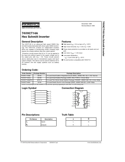
SN54HCT74, SN74HCT74
DUAL DĆTYPE POSITIVEĆEDGEĆTRIGGERED FLIPĆFLOPS
WITH CLEAR AND PRESET
SCLS169E − DECEMBER 1982 − REVISED APRIL 2004
1POST OFFICE BOX 655303 • DALLAS, TEXAS 75265DOperating Voltage Range of 4.5 V to 5.5 V
DOutputs Can Drive Up To 10 LSTTL Loads
DLow Power Consumption, 40-µA Max ICCDTypical tpd = 17 ns
D±4-mA Output Drive at 5 V
DLow Input Current of 1 µA Max
DInputs Are TTL-Voltage Compatible
description/ordering information
The ’HCT74 devices contain two independent
D-type positive-edge-triggered flip-flops. A low
level at the preset (PRE) or clear (CLR) inputs sets
or resets the outputs, regardless of the levels of
the other inputs. When PRE and CLR are inactive
(high), data at the data (D) input meeting the setup
time requirements are transferred to the outputs
on the positive-going edge of the clock (CLK)
pulse. Clock triggering occurs at a voltage level
and is not directly related to the rise time of CLK.
Following the hold-time interval, data at the
Dinput may be changed without affecting the
levels at the outputs.
ORDERING INFORMATION
TAPACKAGE†ORDERABLE
PART NUMBERTOP-SIDE
MARKING
PDIP − NTube of 25SN74HCT74NSN74HCT74N
Tube of 50SN74HCT74D
Reel of 2500SN74HCT74DRSOIC − D
Reel of 250SN74HCT74DTHCT74
°°SOP − NSReel of 2000SN74HCT74NSRHCT74−40C to 85C
SSOP − DBReel of 2000SN74HCT74DBRHT74
Tube of 90SN74HCT74PW
Reel of 2000SN74HCT74PWRTSSOP − PW
Reel of 250SN74HCT74PWTHT74
CDIP − JTube of 25SNJ54HCT74JSNJ54HCT74J
°°CFP − WTube of 150SNJ54HCT74WSNJ54HCT74W−55C to 125C
LCCC − FKTube of 55SNJ54HCT74FKSNJ54HCT74FK
†Package drawings, standard packing quantities, thermal data, symbolization, and PCB design guidelines are
available at www.ti.com/sc/package.
Please be aware that an important notice concerning availability, standard warranty, and use in critical applications of
TexasInstruments semiconductor products and disclaimers thereto appears at the end of this data sheet.1
2
3
4
5
6
714
13
12
11
10
9
81CLR
1D
1CLK
1PRE
1Q
1Q
GNDVCC
2CLR
2D
2CLK
2PRE
2Q
2QSN54HCT74...J OR W PACKAGE
SN74HCT74...D, DB, N, NS, OR PW PACKAGE
(TOP VIEW)
3212019
9101112134
5
6
7
818
17
16
15
142D
NC
2CLK
NC
2PRE1CLK
NC
1PRE
NC
1Q1D1CLR
NC
2Q2QV2CLR
1Q
GNDNCSN54HCT74...FK PACKAGE
(TOP VIEW)
CC
NC − No internal connection
Copyright 2004, Texas Instruments IncorporatedUNLESS OTHERWISE NOTED this document contains PRODUCTIONDATA information current as of publication date. Products conform tospecifications per the terms of Texas Instruments standard warranty.Production processing does not necessarily include testing of allparameters.元器件交易网www.cecb2b.comSN54HCT74, SN74HCT74
DUAL DĆTYPE POSITIVEĆEDGEĆTRIGGERED FLIPĆFLOPS
WITH CLEAR AND PRESET
SCLS169E − DECEMBER 1982 − REVISED APRIL 2004
2POST OFFICE BOX 655303 • DALLAS, TEXAS 75265FUNCTION TABLE
INPUTSOUTPUT
PRECLRCLKDQQ
LHXXHL
HLXXLH
LLXXH†H†
HH°HHL
HH°LLH
HHLXQ0Q0
†This configuration is nonstable; that is, it does not
persist when PRE or CLR returns to its inactive
(high) level.
logic diagram (positive logic)
PRE
CLK
D
CLRQ
QC
CC
C
C
CC
CC
CTG
TGTGTG
absolute maximum ratings over operating free-air temperature range (unless otherwise noted)‡
Supply voltage range, VCC −0.5 V to 7 V. . . . . . . . . . . . . . . . . . . . . . . . . . . . . . . . . . . . . . . . . . . . . . . . . . . . . . . . . .
Input clamp current, IIK (VI < 0 or VI > VCC) (see Note 1) ±20 mA. . . . . . . . . . . . . . . . . . . . . . . . . . . . . . . . . . . .
Output clamp current, IOK (VO < 0 or VO > VCC) (see Note 1) ±20 mA. . . . . . . . . . . . . . . . . . . . . . . . . . . . . . . .
Continuous output current, IO (VO = 0 to VCC) ±25 mA. . . . . . . . . . . . . . . . . . . . . . . . . . . . . . . . . . . . . . . . . . . . . .
Continuous current through VCC or GND ±50 mA. . . . . . . . . . . . . . . . . . . . . . . . . . . . . . . . . . . . . . . . . . . . . . . . . . .
Package thermal impedance, θJA (see Note 2):D package 86°C/W. . . . . . . . . . . . . . . . . . . . . . . . . . . . . . . . . . .
DB package 96°C/W. . . . . . . . . . . . . . . . . . . . . . . . . . . . . . . . .
N package 80°C/W. . . . . . . . . . . . . . . . . . . . . . . . . . . . . . . . . . .
NS package 76°C/W. . . . . . . . . . . . . . . . . . . . . . . . . . . . . . . . .
PW package 113°C/W. . . . . . . . . . . . . . . . . . . . . . . . . . . . . . . .
Storage temperature range, Tstg −65°C to 150°C. . . . . . . . . . . . . . . . . . . . . . . . . . . . . . . . . . . . . . . . . . . . . . . . . . .
‡Stresses beyond those listed under “absolute maximum ratings” may cause permanent damage to the device. These are stress ratings only, and
functional operation of the device at these or any other conditions beyond those indicated under “recommended operating conditions” is not