FMD FT24C16A
- 格式:pdf
- 大小:289.15 KB
- 文档页数:20
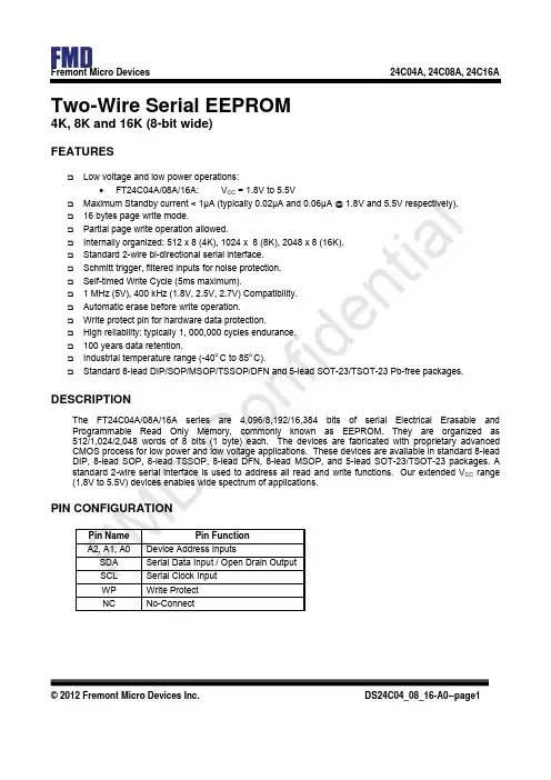
Two-Wire Serial EEPROM4K, 8K and 16K (8-bit wide)FEATURES❑Low voltage and low power operations:FT24C04A/08A/16A: V CC = 1.8V to 5.5V❑Maximum Standby current < 1µA (typically 0.02µA and 0.06µA @ 1.8V and 5.5V respectively).❑16 bytes page write mode.❑Partial page write operation allowed.❑Internally organized: 512 x 8 (4K), 1024 x 8 (8K), 2048 x 8 (16K).❑Standard 2-wire bi-directional serial interface.❑Schmitt trigger, filtered inputs for noise protection.❑Self-timed Write Cycle (5ms maximum).❑ 1 MHz (5V), 400 kHz (1.8V, 2.5V, 2.7V) Compatibility.❑Automatic erase before write operation.❑Write protect pin for hardware data protection.❑High reliability: typically 1, 000,000 cycles endurance.❑100 years data retention.❑Industrial temperature range (-40o C to 85o C).❑Standard 8-lead DIP/SOP/MSOP/TSSOP/DFN and 5-lead SOT-23/TSOT-23 Pb-free packages. DESCRIPTIONThe FT24C04A/08A/16A series are 4,096/8,192/16,384 bits of serial Electrical Erasable and Programmable Read Only Memory, commonly known as EEPROM. They are organized as 512/1,024/2,048 words of 8 bits (1 byte) each. The devices are fabricated with proprietary advanced CMOS process for low power and low voltage applications. These devices are available in standard 8-lead DIP, 8-lead SOP, 8-lead TSSOP, 8-lead DFN, 8-lead MSOP, and 5-lead SOT-23/TSOT-23packages. A standard 2-wire serial interface is used to address all read and write functions. Our extended V CC range(1.8V to 5.5V)devices enables wide spectrum of applications.PIN CONFIGURATIONPin Name Pin FunctionA2, A1, A0 Device Address InputsSDA Serial Data Input / Open Drain OutputSCL Serial Clock InputWP Write ProtectNo-ConnectNC© 2012 Fremont Micro Devices Inc. DS24C04_08_16-A0--page1© 2012 Fremont Micro Devices Inc. DS24C04_08_16-A0--page2All these packaging types come in conventional or Pb-free certified.VCC W P SCL SDAA2A1A0G 8L DIP 8L SOP8L TSSOP W P VCCG ND FT24C04A/08A/16A 5L SOT-23SCL 8L DFN8L M SOP 5L TSO T-23ABSOLUTE MAXIMUM RATINGSIndustrial operating temperature: -40℃ to 85℃ Storage temperature:-50℃ to 125℃Input voltage on any pin relative to ground: -0.3V to V CC + 0.3V Maximum voltage: 8VESD protection on all pins: >2000V* Stresses exceed those listed under “Absolute Maximum Rating” may cause permanent damage to the device. Functional operation of the device at conditions beyond those listed in the specification is not guaranteed. Prolonged exposure to extreme conditions may affect device reliability or functionality .PIN DESCRIPTIONS(A) SERIAL CLOCK (SCL)The rising edge of this SCL input is to latch data into the EEPROM device while the falling edge of thisclock is to clock data out of the EEPROM device.(B) DEVICE / CHIP SELECT ADDRESSES (A2, A1, A0)These are the chip select input signals for the serial EEPROM devices. Typically, these signals are hardwired to either V IH or V IL. If left unconnected, they are internally recognized as V IL. FT24C04A has A0 pin as no-connect. FT24C08A has both A0 and A1 pins as no-connect. For FT24C16A, all device address pins (A0-A2) are no-connect.(C) SERIAL DATA LINE (SDA)SDA data line is a bi-directional signal for the serial devices. It is an open drain output signal and can be wired-OR with other open-drain output devices.(D) WRITE PROTECT (WP)The FT24C04A/08A/16A devices have a WP pin to protect the whole EEPROM array from programming.Programming operations are allowed if WP pin is left un-connected or input to V IL. Conversely all programming functions are disabled if WP pin is connected to V IH or V CC. Read operations is not affected by the WP pin’s input level.Table A© 2012 Fremont Micro Devices Inc. DS24C04_08_16-A0--page3Device Chip Select/DeviceAddress Pins UsedNo-Connect PinsMax number of similardevices on the samebusFT24C04A A2,A1 A0 4 FT24C08A A2, A1,A0 2 FT24C16A (None) A2, A1, A0 1MEMORY ORGANIZATIONThe FT24C04A/08A/16A devices have 32/64/128 pages respectively. Since each page has 16 bytes, random word addressing to FT24C04A/08A/16A will require 9/10/11 bits data word addresses respectively.DEVICE OPERATION(A) SERIAL CLOCK AND DATA TRANSITIONSThe SDA pin is typically pulled to high by an external resistor. Data is allowed to change only when Serial clock SCL is at V IL. Any SDA signal transition may interpret as either a START or STOP condition as described below.(B) START CONDITIONWith SCL V IH, a SDA transition from high to low is interpreted as a START condition. All valid commands must begin with a START condition.© 2012 Fremont Micro Devices Inc. DS24C04_08_16-A0--page4© 2012 Fremont Micro Devices Inc. DS24C04_08_16-A0--page5(C) STOP CONDITIONWith SCL V IH , a SDA transition from low to high is interpreted as a STOP condition. All valid read or write commands end with a STOP condition. The device goes into the STANDBY mode if it is after a read command. A STOP condition after page or byte write command will trigger the chip into the STANDBY mode after the self-timed internal programming finish. (D) ACKNOWLEDGEThe 2-wire protocol transmits address and data to and from the EEPROM in 8 bit words. The EEPROM acknowledges the data or address by outputting a "0" after receiving each word. The ACKNOWLEDGE signal occurs on the 9th serial clock after each word. (E) STANDBY MODEThe EEPROM goes into low power STANDBY mode after a fresh power up, after receiving a STOP bit in read mode, or after completing a self-time internal programming operation.Figure 1: Timing diagram for START and STOP conditionsFigure 2: Timing diagram for output ACKNOWLEDGESCLSDASTART ConditionSTOP ConditionData Data Valid TransitionSCLData inData out START ConditionACKDEVICE ADDRESSINGThe 2-wire serial bus protocol mandates an 8 bits device address word after a START bit condition to invoke valid read or write command. The first four most significant bits of the device address must be 1010, which is common to all serial EEPROM devices. The next three bits are device address bits. These three device address bits (5th, 6th and 7th) are to match with the external chip select/address pin states. If a match is made, the EEPROM device outputs an ACKNOWLEDGE signal after the 8th read/write bit, otherwise the chip will go into STANDBY mode. However, matching may not be needed for some or all device address bits (5th, 6th and 7th) as noted below. The last or 8th bit is a read/write command bit. If the 8th bit is at V IH then the chip goes into read mode. If a “0” is detected, the device enters programming mode.FT24C04A uses A2 (5th) and A1 (6th) device address bits. Only four FT24C04A devices can be wired-OR on the same 2-wire bus. Their corresponding chip select address pins A2 and A1 must be hard wired and coded from 00 (b) to 11 (b). Chip select address pin A0 is not used.FT24C08A uses only A2 (5th) device address bit. Only two FT24C08A devices can be wired-OR on the same 2-wire bus. Their corresponding chip select address pin A2 must be hard-wired and coded from 0 (b) to 1 (b). Chip select address pins A1 and A0 are not used.FT24C16A does not use any device address bit. Only one FT24C16A device can be used on the on 2-wire bus. Chip Select address pins A2, A1, and A0 are not used.WRITE OPERATIONS(A) BYTE WRITEA byte write operation starts when a micro-controller sends a START bit condition, follows by a properEEPROM device address and then a write command. If the device address bits match the chip select address, the EEPROM device will acknowledge at the 9th clock cycle. The micro-controller will then send the rest of the lower 8 bits word address. At the 18th cycle, the EEPROM will acknowledge the 8-bit address word. The micro-controller will then transmit the 8 bit data. Following an ACKNOWLDEGE signal from the EEPROM at the 27th clock cycle, the micro-controller will issue a STOP bit. After receiving the STOP bit, the EEPROM will go into a self-timed programming mode during which all external inputs will be disabled. After a programming time of T WC, the byte programming will finish and the EEPROM device will return to the STANDBY mode.(B) PAGE WRITEA page write is similar to a byte write with the exception that one to sixteen bytes can be programmedalong the same page or memory row. All FT24C04A/08A/16A are organized to have 16 bytes per memory row or page.With the same write command as the byte write, the micro-controller does not issue a STOP bit after sending the 1st byte data and receiving the ACKNOWLEDGE signal from the EEPROM on the 27th clock cycle. Instead it sends out a second 8-bit data word, with the EEPROM acknowledging at the 36th cycle.This data sending and EEPROM acknowledging cycle repeats until the micro-controller sends a STOP bit after the n 9th clock cycle. After which the EEPROM device will go into a self-timed partial or full page programming mode. After the page programming completes after a time of T WC, the devices will return to the STANDBY mode.© 2012 Fremont Micro Devices Inc. DS24C04_08_16-A0--page6The least significant 4 bits of the word address (column address) increments internally by one afterreceiving each data word. The rest of the word address bits (row address) do not change internally, butpointing to a specific memory row or page to be programmed. The first page write data word can be ofany column address. Up to 16 data words can be loaded into a page. If more then 16 data words areloaded, the 17th data word will be loaded to the 1st data word column address. The 18th data word willbe loaded to the 2nd data word column address and so on. In other word, data word address (columnaddress) will “roll” over the previously loaded data.(C) ACKNOWLEDGE POLLINGACKNOWLEDGE polling may be used to poll the programming status during a self-timed internalprogramming. By issuing a valid read or write address command, the EEPROM will not acknowledge atthe 9th clock cycle if the device is still in the self-timed programming mode. However, if the programmingcompletes and the chip has returned to the STANDBY mode, the device will return a validACKNOWLEDGE signal at the 9th clock cycle.READ OPERATIONSThe read command is similar to the write command except the 8th read/write bit in address word is set to “1”.The three read operation modes are described as follows:(A) CURRENT ADDRESS READThe EEPROM internal address word counter maintains the last read or write address plus one if thepower supply to the device has not been cut off. To initiate a current address read operation, the micro-controller issues a START bit and a valid device address word with the read/write bit (8th) set to “1”. TheEEPROM will response with an ACKNOWLEDGE signal on the 9th serial clock cycle. An 8-bit data wordwill then be serially clocked out. The internal address word counter will then automatically increase byone. For current address read the micro-controller will not issue an ACKNOWLEDGE signal on the 18thclock cycle. The micro-controller issues a valid STOP bit after the 18th clock cycle to terminate the readoperation. The device then returns to STANDBY mode.(B) SEQUENTIAL READThe sequential read is very similar to current address read. The micro-controller issues a START bitand a valid device address word with read/write bit (8th) set to “1”. The EEPROM will response with anACKNOWLEDGE signal on the 9th serial clock cycle. An 8-bit data word will then be serially clocked out.Meanwhile the internally address word counter will then automatically increase by one. Unlike currentaddress read, the micro-controller sends an ACKNOWLEDGE signal on the 18th clock cycle signalingthe EEPROM device that it wants another byte of data. Upon receiving the ACKNOWLEDGE signal, theEEPROM will serially clocked out an 8-bit data word based on the incremented internal address counter.If the micro-controller needs another data, it sends out an ACKNOWLEDGE signal on the 27th clockcycle. Another 8-bit data word will then be serially clocked out. This sequential read continues as longas the micro-controller sends an ACKNOWLEDGE signal after receiving a new data word. When theinternal address counter reaches its maximum valid address, it rolls over to the beginning of the memoryarray address. Similar to current address read, the micro-controller can terminate the sequential read bynot acknowledging the last data word received, but sending a STOP bit afterwards instead.(C) RANDOM READRandom read is a two-steps process. The first step is to initialize the internal address counter with atarget read address using a “dummy write” instruction. The second step is a current address read.To initialize the internal address counter with a target read address, the micro-controller issues a STARTbit first, follows by a valid device address with the read/write bit (8th) set to “0”. The EEPROM will thenacknowledge. The micro-controller will then send the address word. Again the EEPROM willacknowledge. Instead of sending a valid written data to the EEPROM, the micro-controller performs a current address read© 2012 Fremont Micro Devices Inc. DS24C04_08_16-A0--page7instruction to read the data. Note that once a START bit is issued, the EEPROM will reset the internal programming process and continue to execute the new instruction - which is to read the current address.© 2012 Fremont Micro Devices Inc. DS24C04_08_16-A0--page8© 2012 Fremont Micro Devices Inc. DS24C04_08_16-A0--page9Figure 8: SCL and SDA Bus TimingAC CHARACTERISTICS1.8 V2.5-5.0 V Symbol ParameterMin Max Min Max Unit f SCL Clock frequency, SCL 400 1000 kHz t LOW Clock pulse width low 1.20.7µst HIGH Clock pulse width high0.4 0.3 µst I Noise suppression time (1) 180 120 ns t AA Clock low to data out valid 0.3 0.9 0.2 0.7 µs t BUF Time the bus must be free before a new transmission can start (1)1.3 0.5 µs t HD.STA START hold time 0.6 0.25 µs t SU.STA START set-up time 0.6 0.25 µs t HD.DAT Data in hold time 0 0 µs t SU.DAT Data in set-up time 100100nst R Input rise time (1)0.3 0.3 µs t F Input fall time (1) 300 100 nst SU.STO STOP set-up time 0.6 0.25 µs t DH Date out hold time 50 50 ns WRWrite cycle time55msEndurance(1)25o C, Page Mode, 3.3V1,000,000Write CyclesNotes: 1. This Parameter is expected by characterization but are not fully screened by test.2. AC Measurement conditions: R L (Connects to Vcc): 1.3K ΩInput Pulse Voltages: 0.3Vcc to 0.7VccInput and output timing reference Voltages: 0.5VccDC CHARACTERISTICSSymbol Parameter TestConditions MinTypicalMaxUnitsV CC124C A supplyV CC1.8 5.5 VI CC Supply read current V CC@ 5.0V SCL = 400 kHz 0.5 1.0 mA I CC Supply write current V CC@ 5.0V SCL = 400 kHz 2.0 3.0 mA I SB1 Supplycurrent V CC@ 1.8V, V IN = V CC or V SS 1.0 µA I SB2 Supplycurrent V CC@ 2.5V, V IN = V CC or V SS 1.0 µA I SB3 Supplycurrent V CC@ 5.0V, V IN = V CC or V SS0.06 1.0 µAI IL Input leakagecurrentV IN = V CC or V SS 3.0 µAI LO Output leakagecurrentV IN = V CC or V SS 3.0 µAV IL Input low level -0.6 V CC x0.3 V V IH Input high level V CC x0.7V CC+0.5 V V OL1 Outputlowlevel V CC@ 1.8V, I OL = 0.15 mA 0.2 V V OL2 Outputlowlevel V CC@ 3.0V, I OL = 2.1 mA 0.4 V© 2012 Fremont Micro Devices Inc. DS24C04_08_16-A0--page10© 2012 Fremont Micro Devices Inc. DS24C04_08_16-A0--page11ORDERING INFORMATION:Density PackageTemperatureRangeVcc HSF Packaging Ordering CodeRoHSTube FT24C04A-UDR-B DIP8 -40℃-85℃ 1.8V-5.5VGreen Tube FT24C04A-UDG-B Tube FT24C04A-USR-B RoHSTape and Reel FT24C04A-USR-TTube FT24C04A-USG-B SOP8 -40℃-85℃ 1.8V-5.5VGreen Tape and Reel FT24C04A-USG-TTube FT24C04A-UMR-B RoHSTape and Reel FT24C04A-UMR-TTube FT24C04A-UMG-B MSOP8 -40℃-85℃ 1.8V-5.5VGreenTape and Reel FT24C04A-UMG-TTube FT24C04A-UTR-B RoHSTape and Reel FT24C04A-UTR-TTube FT24C04A-UTG-B TSSOP8 -40℃-85℃ 1.8V-5.5VGreenTape and Reel FT24C04A-UTG-T RoHS Tape and Reel FT24C04A-ULR-T SOT23-5 -40℃-85℃ 1.8V-5.5V Green Tape and Reel FT24C04A-ULG-T RoHS Tape and Reel FT24C04A-UPR-T TSOT23-5 -40℃-85℃ 1.8V-5.5V Green Tape and Reel FT24C04A-UPG-T RoHS Tape and Reel FT24C04A-UNR-T 4kbitsDFN8 -40℃-85℃ 1.8V-5.5V Green Tape and Reel FT24C04A-UNG-TRoHS Tube FT24C08A-UDR-B DIP8 -40℃-85℃ 1.8V-5.5VGreen Tube FT24C08A-UDG-B Tube FT24C08A-USR-B RoHSTape and Reel FT24C08A-USR-TTube FT24C08A-USG-B 8kbitsSOP8 -40℃-85℃ 1.8V-5.5VGreenTape and Reel FT24C08A-USG-TD: DIP8 S: SOP8 M: MSOP8 T: TSSOP8 L: SOT23-5 P: TSOT23-5 N: DFN8Packaging B: TubeT: Tape and Reel HSF R: RoHS G: GreenU:-40© 2012 Fremont Micro Devices Inc. DS24C04_08_16-A0--page12Density Package TemperatureRangeVcc HSF Packaging Ordering CodeTube FT24C08A-UMR-BRoHSTape and Reel FT24C08A-UMR-TTube FT24C08A-UMG-B MSOP8 -40℃-85℃ 1.8V-5.5VGreen Tape and Reel FT24C08A-UMG-TTube FT24C08A-UTR-B RoHSTape and Reel FT24C08A-UTR-TTube FT24C08A-UTG-B TSSOP8 -40℃-85℃ 1.8V-5.5VGreen Tape and Reel FT24C08A-UTG-T RoHSTape and Reel FT24C08A-ULR-T SOT23-5 -40℃-85℃ 1.8V-5.5V Green Tape and Reel FT24C08A-ULG-T RoHS Tape and Reel FT24C08A-UPR-T TSOT23-5 -40℃-85℃ 1.8V-5.5V Green Tape and Reel FT24C08A-UPG-T RoHS Tape and Reel FT24C08A-UNR-T 8kbitsDFN8 -40℃-85℃ 1.8V-5.5V Green Tape and Reel FT24C08A-UNG-TRoHS Tube FT24C16A-UDR-B DIP8 -40℃-85℃ 1.8V-5.5VGreen Tube FT24C16A-UDG-B Tube FT24C16A-USR-B RoHSTape and Reel FT24C16A-USR-TTube FT24C16A-USG-B SOP8 -40℃-85℃ 1.8V-5.5VGreen Tape and Reel FT24C16A-USG-TTube FT24C16A-UMR-B RoHSTape and Reel FT24C16A-UMR-TTube FT24C16A-UMG-B MSOP8 -40℃-85℃ 1.8V-5.5VGreenTape and Reel FT24C16A-UMG-TTube FT24C16A-UTR-B RoHSTape and Reel FT24C16A-UTR-TTube FT24C16A-UTG-B TSSOP8 -40℃-85℃ 1.8V-5.5VGreenTape and Reel FT24C16A-UTG-T RoHS Tape and Reel FT24C16A-ULR-T SOT23-5 -40℃-85℃ 1.8V-5.5V Green Tape and Reel FT24C16A-ULG-T RoHS Tape and Reel FT24C16A-UPR-T TSOT23-5 -40℃-85℃ 1.8V-5.5V Green Tape and Reel FT24C16A-UPG-T RoHS Tape and Reel FT24C16A-UNR-T 16kbitsDFN8 -40℃-85℃ 1.8V-5.5VGreenTape and Reel FT24C16A-UNG-TDIP8 PACKAGE OUTLINEDIMENSIONSDimensions In Millimeters Dimensions In InchesSymbolMin Max Min MaxA 3.710 4.310 0.146 0.170A1 0.510 0.020A2 3.200 3.600 0.126 0.142B 0.380 0.570 0.015 0.0221.524(BSC) 0.060(BSC)B1C 0.204 0.360 0.008 0.014D 9.000 9.400 0.354 0.370E 6.200 6.600 0.244 0.260E1 7.320 7.920 0.288 0.312(BSC) 0.100(BSC)e 2.540L 3.000 3.600 0.118 0.142E2 8.400 9.000 0.331 0.354© 2012 Fremont Micro Devices Inc. DS24C04_08_16-A0--page13SOP8 PACKAGE OUTLINE DIMENSIONSDimensions In Millimeters Dimensions In InchesSymbolMin Max Min MaxA 1.350 1.750 0.053 0.069A1 0.100 0.250 0.004 0.010A2 1.350 1.550 0.053 0.061b 0.330 0.510 0.013 0.020c 0.170 0.250 0.006 0.010D 4.700 5.100 0.185 0.200E 3.800 4.000 0.150 0.157E1 5.800 6.200 0.228 0.244(BSC)(BSC) 0.050e 1.270L 0.400 1.270 0.016 0.050θ0° 8° 0° 8°© 2012 Fremont Micro Devices Inc. DS24C04_08_16-A0--page14MSOP8 PACKAGE OUTLINE DIMENSIONSDimensions In Millimeters Dimensions In InchesSymbolMin Max Min MaxA 0.820 1.100 0.320 0.043A1 0.020 0.150 0.001 0.006A2 0.750 0.950 0.030 0.037b 0.250 0.380 0.010 0.015c 0.090 0.230 0.004 0.009D 2.900 3.100 0.114 0.122e 0.65 (BSC) 0.026 (BSC)E 2.900 3.100 0.114 0.122E1 4.750 5.050 0.187 0.199L 0.400 0.800 0.016 0.031θ0° 6° 0° 6°© 2012 Fremont Micro Devices Inc. DS24C04_08_16-A0--page15TSSOP8 PACKAGE OUTLINEDIMENSIONSDimensions In Millimeters Dimensions In InchesSymbolMin Max Min MaxD 2.900 3.100 0.114 0.122E 4.300 4.500 0.169 0.177b 0.190 0.300 0.007 0.012c 0.090 0.200 0.004 0.008E1 6.250 6.550 0.246 0.258A 1.100 0.043A2 0.800 1.000 0.031 0.039A1 0.020 0.150 0.001 0.006e 0.65 (BSC) 0.026 (BSC)L 0.500 0.700 0.020 0.028H 0.25 (TYP) 0.01 (TYP)θ 1° 7° 1° 7°© 2012 Fremont Micro Devices Inc. DS24C04_08_16-A0--page16SOT-23-5 PACKAGE OUTLINE DIMENSIONSDimensions In Millimeters Dimensions In InchesSymbolMin Max Min MaxA 1.050 1.250 0.041 0.049A1 0.000 0.100 0.000 0.004A2 1.050 1.150 0.041 0.045b 0.300 0.500 0.012 0.020c 0.100 0.200 0.004 0.008D 2.820 3.020 0.111 0.119E 1.500 1.700 0.059 0.067E1 2.650 2.950 0.104 0.116e 0.95 (BSC) 0.037 (BSC)e1 1.800 2.000 0.071 0.079L 0.300 0.600 0.012 0.024θ 0° 8° 0° 6°© 2012 Fremont Micro Devices Inc. DS24C04_08_16-A0--page17TSOT-23-5 PACKAGE OUTLINE DIMENSIONSDimensions In Millimeters Dimensions In InchesSymbolMin Max Min MaxA 0.700 0.900 0.028 0.035A1 0.000 0.100 0.000 0.004A2 0.700 0.800 0.028 0.031b 0.350 0.500 0.014 0.020c 0.080 0.200 0.003 0.008D 2.820 3.020 0.111 0.119E 1.600 1.700 0.063 0.067E1 2.650 2.950 0.104 0.116e 0.95 (BSC) 0.037 (BSC)e1 1.90 (BSC) 0.075 (BSC)L 0.300 0.600 0.012 0.024θ 0° 8° 0° 8°© 2012 Fremont Micro Devices Inc. DS24C04_08_16-A0--page18DFN8 PACKAGE OUTLINE DIMENSIONSDimensions In MillimetersSymbolMin Nom Max0.75 0.80A 0.700.02 0.05A1 -0.25 0.03b 0.180.20 0.25c 0.182.00 2.10D 1.90D2 1.50REFe 0.50BSCNd 1.50BSC3.10E 2.903.00E2 1.60REF0.40 0.50L 0.300.25 0.30h 0.20© 2012 Fremont Micro Devices Inc. DS24C04_08_16-A0--page19Fremont Micro Devices (SZ) Limited#5-8, 10/F, Changhong Building, Ke-Ji Nan 12 Road, Nanshan District, ShenzhenTel: (86 755) 86117811Fax: (86 755) 86117810Fremont Micro Devices (Hong Kong) Limited#16, 16/F, Blk B, Veristrong Industrial Centre, 34-36 Au Pui Wan Street, Fotan, Shatin, Hong KongTel: (852) 27811186Fax: (852) 27811144Fremont Micro Devices (USA), Inc.42982 Osgood Road Fremont, CA 94539Tel: (1-510) 668-1321Fax: (1-510) 226-9918Web Site: /* Information furnished is believed to be accurate and reliable. However, Fremont Micro Devices, Incorporated (BVI) assumes no responsibility for the consequences of use of such information or for any infringement of patents of other rights of third parties which may result from its use. No license is granted by implication or otherwise under any patent rights of Fremont Micro Devices, Incorporated (BVI). Specifications mentioned in this publication are subject to change without notice. This publication supersedes and replaces all information previously supplied. Fremont Micro Devices, Incorporated (BVI) products are not authorized for use as critical components in life support devices or systems without express written approval of Fremont Micro Devices, Incorporated (BVI). The FMD logo is a registered trademark of Fremont Micro Devices, Incorporated (BVI). All other names are the property of their respective owners.© 2012 Fremont Micro Devices Inc. DS24C04_08_16-A0--page20。