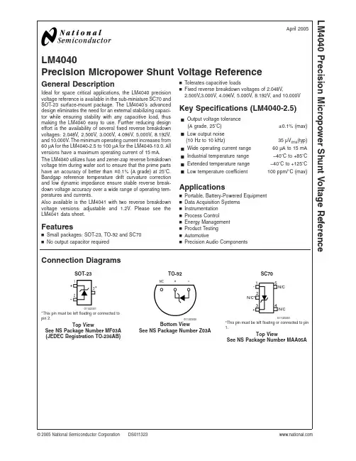
LM2700_04中文资料
- 格式:pdf
- 大小:521.33 KB
- 文档页数:17
LM2700600kHz/1.25MHz,2.5A,Step-up PWM DC/DC ConverterGeneral DescriptionThe LM2700is a step-up DC/DC converter with a 3.6A,80m Ωinternal switch and pin selectable operating fre-quency.With the ability to produce 500mA at 8V from a single Lithium Ion battery,the LM2700is an ideal part for biasing LCD displays.The LM2700can be operated at switching frequencies of 600kHz and 1.25MHz allowing for easy filtering and low noise.An external compensation pin gives the user flexibility in setting frequency compensation,which makes possible the use of small,low ESR ceramic capacitors at the output.The LM2700features continuous switching at light loads and operates with a switching quies-cent current of 2.0mA at 600kHz and 3.0mA at 1.25MHz.The LM2700is available in a low profile 14-lead TSSOP package or a 14-lead LLP package.Featuresn 3.6A,0.08Ω,internal switchn Operating input voltage range of 2.2V to 12V n Input undervoltage protectionn Adjustable output voltage up to 17.5Vn 600kHz/1.25MHz pin selectable frequency operation n Over temperature protectionnSmall 14-Lead TSSOP or LLP packageApplicationsn LCD Bias Supplies n Handheld Devices n Portable Applications n GSM/CDMA Phones nDigital CamerasTypical Application Circuit20012301600kHz OperationMay 2004LM2700600kHz/1.25MHz,2.5A,Step-up PWM DC/DC Converter©2004National Semiconductor Corporation Connection DiagramTop View2001230414-Lead TSSOP or LLPOrdering InformationOrder Number Package Type NSC Package DrawingSupplied AsLM2700MT-ADJ TSSOP-14MTC1494Units,RailLM2700MTX-ADJ TSSOP-14MTC142500Units,Tape and Reel LM2700LD-ADJ LLP-14LDA14A 1000Units,Tape and Reel LM2700LDX-ADJLLP-14LDA14A4500Units,Tape and ReelPin DescriptionPin Name Function1V C Compensation network connection.Connected to the output of the voltage error amplifier.2FB Output voltage feedback input.3SHDN Shutdown control input,active low.4AGND Analog ground.5PGND Power ground.PGND pins must be connected together directly at the part.6PGND Power ground.PGND pins must be connected together directly at the part.7PGND Power ground.PGND pins must be connected together directly at the part.8SW Power switch input.Switch connected between SW pins and PGND pins.9SW Power switch input.Switch connected between SW pins and PGND pins.10SW Power switch input.Switch connected between SW pins and PGND pins.11NC Pin not connected internally.12V IN Analog power input.13FSLCT Switching frequency select input.V IN =1.25MHz.Ground =600kHz.14NCConnect to ground.L M 2700 2Block Diagram20012303Detailed DescriptionThe LM2700utilizes a PWM control scheme to regulate the output voltage over all load conditions.The operation can best be understood referring to the block diagram and Figure 1of the Operation section.At the start of each cycle,the oscillator sets the driver logic and turns on the NMOS power device conducting current through the inductor,cycle1of Figure1(a).During this cycle,the voltage at the V C pin controls the peak inductor current.The V C voltage will in-crease with larger loads and decrease with smaller.This voltage is compared with the summation of the SW voltage and the ramp compensation.The ramp compensation is used in PWM architectures to eliminate the sub-harmonic oscillations that occur during duty cycles greater than50%. Once the summation of the ramp compensation and switch voltage equals the V C voltage,the PWM comparator resetsthe driver logic turning off the NMOS power device.Theinductor current then flows through the schottky diode to theload and output capacitor,cycle2of Figure1(b).The NMOSpower device is then set by the oscillator at the end of theperiod and current flows through the inductor once again.The LM2700has dedicated protection circuitry running dur-ing normal operation to protect the IC.The Thermal Shut-down circuitry turns off the NMOS power device when thedie temperature reaches excessive levels.The UVP com-parator protects the NMOS power device during supplypower startup and shutdown to prevent operation at voltagesless than the minimum input voltage.The OVP comparator isused to prevent the output voltage from rising at no loadsallowing full PWM operation over all load conditions.TheLM2700also features a shutdown mode decreasing thesupply current to5µA.LM27003Absolute Maximum Ratings (Note 2)If Military/Aerospace specified devices are required,please contact the National Semiconductor Sales Office/Distributors for availability and specifications.V IN12V SW Voltage 18V FB Voltage 7VV C Voltage0.965V ≤V C ≤1.565VSHDN Voltage (Note 1)7V FSLCT (Note 1)12V Maximum Junction Temperature 150˚CPower Dissipation(Note 3)Internally LimitedLead Temperature 300˚C Vapor Phase (60sec.)215˚CInfrared (15sec.)220˚C ESD Susceptibility (Note 4)Human Body Model 2kV Machine Model200VOperating ConditionsOperating Junction Temperature Range (Note 5)−40˚C to +125˚C Storage Temperature −65˚C to +150˚CSupply Voltage 2.2V to 12VSW Voltage17.5VElectrical CharacteristicsSpecifications in standard type face are for T J =25˚C and those with boldface type apply over the full Operating Tempera-ture Range (T J =−40˚C to +125˚C)Unless otherwise specified.V IN =2.2V and I L =0A,unless otherwise specified.Symbol ParameterConditionsMin (Note 5)Typ (Note 6)Max (Note 5)Units I QQuiescent CurrentFB =2.2V (Not Switching)FSLCT =0V1.22mA FB =2.2V (Not Switching)FSLCT =V IN 1.32mA V SHDN =0V520µA V FBFeedback Voltage 1.2285 1.26 1.2915V I CL (Note 7)Switch Current Limit V IN =2.7V (Note 8) 2.55 3.6 4.3A %V FB /∆V IN Feedback Voltage Line Regulation2.2V ≤V IN ≤12.0V0.020.07%/VI B FB Pin Bias Current (Note 9)0.540nA V IN Input Voltage Range2.212V g m Error Amp Transconductance ∆I =5µA 40155290µmho A V Error Amp Voltage Gain 135V/V D MAX Maximum Duty Cycle FSLCT =Ground 7885%D MIN Minimum Duty Cycle FSLCT =Ground 15%FSLCT =V IN 30f S Switching Frequency FSLCT =Ground 480600720kHz FSLCT =V IN 1 1.25 1.5MHz I SHDN Shutdown Pin Current V SHDN =V IN 0.0081µA V SHDN =0V −0.5−1I L Switch Leakage Current V SW =18V0.0220µA R DSON Switch R DSON (Note 10)V IN =2.7V,I SW =2A 80150m ΩTh SHDN SHDN Threshold Output High 0.90.6V Output Low0.60.3V UVP On Threshold 1.95 2.05 2.2V Off Threshold 1.85 1.95 2.1V θJAThermal Resistance (Note 11)TSSOP,package only 150˚C/WLLP,package only 45Note 1:This voltage should never exceed V IN .Note 2:Absolute maximum ratings are limits beyond which damage to the device may occur.Operating Ratings are conditions for which the device is intended to be functional,but device parameter specifications may not be guaranteed.For guaranteed specifications and test conditions,see the Electrical Characteristics.L M 2700 4Electrical Characteristics(Continued)Note 3:The maximum allowable power dissipation is a function of the maximum junction temperature,T J (MAX),the junction-to-ambient thermal resistance,θJA ,and the ambient temperature,T A .See the Electrical Characteristics table for the thermal resistance.The maximum allowable power dissipation at any ambient temperature is calculated using:P D (MAX)=(T J(MAX)−T A )/θJA .Exceeding the maximum allowable power dissipation will cause excessive die temperature,and the regulator will go into thermal shutdown.Note 4:The human body model is a 100pF capacitor discharged through a 1.5k Ωresistor into each pin.The machine model is a 200pF capacitor discharged directly into each pin.Note 5:All limits guaranteed at room temperature (standard typeface)and at temperature extremes (bold typeface).All room temperature limits are 100%tested or guaranteed through statistical analysis.All limits at temperature extremes are guaranteed via correlation using standard Statistical Quality Control (SQC)methods.All limits are used to calculate Average Outgoing Quality Level (AOQL).Note 6:Typical numbers are at 25˚C and represent the most likely norm.Note 7:Duty cycle affects current limit due to ramp generator.Note 8:Current limit at 0%duty cycle.See TYPICAL PERFORMANCE section for Switch Current Limit vs.V IN Note 9:Bias current flows into FB pin.Note 10:Does not include the bond wires.Measured directly at the die.Note 11:Refer to National’s packaging website for more detailed thermal information and mounting techniques for the LLP and TSSOP packages.Typical Performance CharacteristicsEfficiency vs.Load Current (V OUT =8V,f S =600kHz)Efficiency vs.Load Current (V OUT =8V,f S =1.25MHz)2001232620012325Efficiency vs.Load Current (V OUT =5V,f S =600kHz)Efficiency vs.Load Current (V OUT =12V,f S =600kHz)2001233420012335LM27005Typical Performance Characteristics(Continued)Switch Current Limit vs.TemperatureSwitch Current Limit vs.V IN2001232020012322R DSON vs.V IN (I SW =2A)I Q vs.V IN(600kHz,not switching)2001232720012328I Q vs.V IN(600kHz,switching)I Q vs.V IN(1.25MHz,not switching)2001232920012321L M 2700 6Typical Performance Characteristics(Continued)I Q vs.V IN(1.25MHz,switching)I Q vs.V IN(In shutdown) 2001231920012318Frequency vs.V IN (600kHz)Frequency vs.V IN(1.25MHz)2001232320012324LM2700 7OperationCONTINUOUS CONDUCTION MODEThe LM2700is a current-mode,PWM boost regulator.Aboost regulator steps the input voltage up to a higher outputvoltage.In continuous conduction mode(when the inductorcurrent never reaches zero at steady state),the boost regu-lator operates in two cycles.In the first cycle of operation,shown in Figure1(a),thetransistor is closed and the diode is reverse biased.Energyis collected in the inductor and the load current is supplied byC OUT.The second cycle is shown in Figure1(b).During this cycle,the transistor is open and the diode is forward biased.Theenergy stored in the inductor is transferred to the load andoutput capacitor.The ratio of these two cycles determines the output voltage.The output voltage is defined approximately as:where D is the duty cycle of the switch,D and D'will berequired for design calculations.SETTING THE OUTPUT VOLTAGEThe output voltage is set using the feedback pin and aresistor divider connected to the output as shown in Figure3.The feedback pin voltage is1.26V,so the ratio of the feed-back resistors sets the output voltage according to the fol-lowing equation:INTRODUCTION TO COMPENSATION20012302FIGURE1.Simplified Boost Converter Diagram(a)First Cycle of Operation(b)Second Cycle Of Operation20012305FIGURE2.(a)Inductor current.(b)Diode current. LM278Operation(Continued)The LM2700is a current mode PWM boost converter.Thesignal flow of this control scheme has two feedback loops,one that senses switch current and one that senses outputvoltage.To keep a current programmed control converter stableabove duty cycles of50%,the inductor must meet certaincriteria.The inductor,along with input and output voltage,will determine the slope of the current through the inductor(see Figure2(a)).If the slope of the inductor current is toogreat,the circuit will be unstable above duty cycles of50%.A4.7µH inductor is recommended for most600kHz appli-cations,while a2.2µH inductor may be used for most1.25MHz applications.If the duty cycle is approaching the maxi-mum of85%,it may be necessary to increase the inductanceby as much as2X.See Inductor and Diode Selection formore detailed inductor sizing.The LM2700provides a compensation pin(V C)to customizethe voltage loop feedback.It is recommended that a seriescombination of R C and C C be used for the compensationnetwork,as shown in Figure3.For any given application,there exists a unique combination of R C and C C that willoptimize the performance of the LM2700circuit in terms ofits transient response.The series combination of R C and C Cintroduces a pole-zero pair according to the following equa-tions:where R O is the output impedance of the error amplifier,approximately850kΩ.For most applications,performancecan be optimized by choosing values within the range5kΩ≤R C≤20kΩ(R C can be up to200kΩif C C2is used,see HighOutput Capacitor ESR Compensation)and680pF≤C C≤4.7nF.Refer to the Applications Information section for rec-ommended values for specific circuits and conditions.Referto the Compensation section for other design requirement.COMPENSATIONThis section will present a general design procedure to helpinsure a stable and operational circuit.The designs in thisdatasheet are optimized for particular requirements.If differ-ent conversions are required,some of the components mayneed to be changed to ensure stability.Below is a set ofgeneral guidelines in designing a stable circuit for continu-ous conduction operation(loads greater than approximately100mA),in most all cases this will provide for stability duringdiscontinuous operation as well.The power components andtheir effects will be determined first,then the compensationcomponents will be chosen to produce stability.INDUCTOR AND DIODE SELECTIONAlthough the inductor sizes mentioned earlier are fine formost applications,a more exact value can be calculated.Toensure stability at duty cycles above50%,the inductor musthave some minimum value determined by the minimuminput voltage and the maximum output voltage.This equa-tion is:where fs is the switching frequency,D is the duty cycle,andR DSON is the ON resistance of the internal switch taken fromthe graph"R DSON vs.V IN"in the Typical Performance Char-acteristics section.This equation is only good for duty cyclesgreater than50%(D>0.5),for duty cycles less than50%therecommended values may be used.The corresponding in-ductor current ripple as shown in Figure2(a)is given by:The inductor ripple current is important for a few reasons.One reason is because the peak switch current will be theaverage inductor current(input current or I LOAD/D’)plus∆i L.As a side note,discontinuous operation occurs when theinductor current falls to zero during a switching cycle,or∆i Lis greater than the average inductor current.Therefore,con-tinuous conduction mode occurs when∆i L is less than theaverage inductor current.Care must be taken to make surethat the switch will not reach its current limit during normaloperation.The inductor must also be sized accordingly.Itshould have a saturation current rating higher than the peakinductor current expected.The output voltage ripple is alsoaffected by the total ripple current.The output diode for a boost regulator must be chosencorrectly depending on the output voltage and the outputcurrent.The typical current waveform for the diode in con-tinuous conduction mode is shown in Figure2(b).The diodemust be rated for a reverse voltage equal to or greater thanthe output voltage used.The average current rating must begreater than the maximum load current expected,and thepeak current rating must be greater than the peak inductorcurrent.During short circuit testing,or if short circuit condi-tions are possible in the application,the diode current ratingmust exceed the switch current ing Schottky diodeswith lower forward voltage drop will decrease power dissipa-tion and increase efficiency.DC GAIN AND OPEN-LOOP GAINSince the control stage of the converter forms a completefeedback loop with the power components,it forms a closed-loop system that must be stabilized to avoid positive feed-back and instability.A value for open-loop DC gain will berequired,from which you can calculate,or place,poles andzeros to determine the crossover frequency and the phasemargin.A high phase margin(greater than45˚)is desired forthe best stability and transient response.For the purpose ofstabilizing the LM2700,choosing a crossover point well be-low where the right half plane zero is located will ensuresufficient phase margin.A discussion of the right half planezero and checking the crossover using the DC gain willfollow.INPUT AND OUTPUT CAPACITOR SELECTIONThe switching action of a boost regulator causes a triangularvoltage waveform at the input.A capacitor is required toreduce the input ripple and noise for proper operation of theregulator.The size used is dependant on the application andboard layout.If the regulator will be loaded uniformly,withLM27009Operation(Continued)very little load changes,and at lower current outputs,theinput capacitor size can often be reduced.The size can alsobe reduced if the input of the regulator is very close to thesource output.The size will generally need to be larger forapplications where the regulator is supplying nearly themaximum rated output or if large load steps are expected.Aminimum value of10µF should be used for the less stressfulcondtions while a33µF or47µF capacitor may be requiredfor higher power and dynamic rger values and/orlower ESR may be needed if the application requires verylow ripple on the input source voltage.The choice of output capacitors is also somewhat arbitraryand depends on the design requirements for output voltageripple.It is recommended that low ESR(Equivalent SeriesResistance,denoted R ESR)capacitors be used such asceramic,polymer electrolytic,or low ESR tantalum.HigherESR capacitors may be used but will require more compen-sation which will be explained later on in the section.TheESR is also important because it determines the peak topeak output voltage ripple according to the approximateequation:∆V OUT)2∆i L R ESR(in Volts)A minimum value of10µF is recommended and may beincreased to a larger value.After choosing the output capaci-tor you can determine a pole-zero pair introduced into thecontrol loop by the following equations:Where R L is the minimum load resistance corresponding tothe maximum load current.The zero created by the ESR ofthe output capacitor is generally very high frequency if theESR is small.If low ESR capacitors are used it can beneglected.If higher ESR capacitors are used see the HighOutput Capacitor ESR Compensation section.RIGHT HALF PLANE ZEROA current mode control boost regulator has an inherent righthalf plane zero(RHP zero).This zero has the effect of a zeroin the gain plot,causing an imposed+20dB/decade on therolloff,but has the effect of a pole in the phase,subtractinganother90˚in the phase plot.This can cause undesirableeffects if the control loop is influenced by this zero.To ensurethe RHP zero does not cause instability issues,the controlloop should be designed to have a bandwidth of less than1⁄2the frequency of the RHP zero.This zero occurs at a fre-quency of:where I LOAD is the maximum load current.SELECTING THE COMPENSATION COMPONENTSThe first step in selecting the compensation components R Cand C C is to set a dominant low frequency pole in the controlloop.Simply choose values for R C and C C within the rangesgiven in the Introduction to Compensation section to set thispole in the area of10Hz to500Hz.The frequency of the polecreated is determined by the equation:where R O is the output impedance of the error amplifier,approximately850kΩ.Since R C is generally much less thanR O,it does not have much effect on the above equation andcan be neglected until a value is chosen to set the zero f ZC.f ZC is created to cancel out the pole created by the outputcapacitor,f P1.The output capacitor pole will shift with differ-ent load currents as shown by the equation,so setting thezero is not exact.Determine the range of f P1over the ex-pected loads and then set the zero f ZC to a point approxi-mately in the middle.The frequency of this zero is deter-mined by:Now R C can be chosen with the selected value for C C.Check to make sure that the pole f PC is still in the10Hz to500Hz range,change each value slightly if needed to ensureboth component values are in the recommended range.Afterchecking the design at the end of this section,these valuescan be changed a little more to optimize performance ifdesired.This is best done in the lab on a bench,checking theload step response with different values until the ringing andovershoot on the output voltage at the edge of the load stepsis minimal.This should produce a stable,high performancecircuit.For improved transient response,higher values of R Cshould be chosen.This will improve the overall bandwidthwhich makes the regulator respond more quickly to tran-sients.If more detail is required,or the most optimal perfor-mance is desired,refer to a more in depth discussion ofcompensating current mode DC/DC switching regulators.HIGH OUTPUT CAPACITOR ESR COMPENSATIONWhen using an output capacitor with a high ESR value,orjust to improve the overall phase margin of the control loop,another pole may be introduced to cancel the zero createdby the ESR.This is accomplished by adding another capaci-tor,C C2,directly from the compensation pin V C to ground,inparallel with the series combination of R C and C C.The poleshould be placed at the same frequency as f Z1,the ESRzero.The equation for this pole follows:To ensure this equation is valid,and that C C2can be usedwithout negatively impacting the effects of R C and C C,f PC2must be greater than10f ZC.CHECKING THE DESIGNThe final step is to check the design.This is to ensure abandwidth of1⁄2or less of the frequency of the RHP zero.This is done by calculating the open-loop DC gain,A DC.Afterthis value is known,you can calculate the crossover visuallyby placing a−20dB/decade slope at each pole,and a+20dB/decade slope for each zero.The point at which the gain plotcrosses unity gain,or0dB,is the crossover frequency.If thecrossover frequency is less than1⁄2the RHP zero,the phasemargin should be high enough for stability.The phase mar-LM2710Operation(Continued)gin can also be improved by adding C C2as discussed earlier in the section.The equation for A DC is given below with additional equations required for the calculation:mc )0.072fs (in V/s)where R L is the minimum load resistance,V IN is the mini-mum input voltage,g m is the error amplifier transconduc-tance found in the Electrical Characteristics table,and R D -SON is the value chosen from the graph "R DSON vs.V IN "in the Typical Performance Characteristics section.LAYOUT CONSIDERATIONSThe LM2700uses two separate ground connections,PGND for the driver and NMOS power device and AGND for the sensitive analog control circuitry.The AGND and PGND pins should be tied directly together at the package.The feed-back and compensation networks should be connected di-rectly to a dedicated analog ground plane and this ground plane must connect to the AGND pin.If no analog ground plane is available then the ground connections of the feed-back and compensation networks must tie directly to the AGND pin.Connecting these networks to the PGND can inject noise into the system and effect performance.The input bypass capacitor C IN ,as shown in Figure 3,must be placed close to the IC.This will reduce copper trace resistance which effects input voltage ripple of the IC.For additional input voltage filtering,a 100nF bypass capacitor can be placed in parallel with C IN ,close to the V IN pin,to shunt any high frequency noise to ground.The output ca-pacitor,C OUT ,should also be placed close to the IC.Any copper trace connections for the C OUT capacitor can in-crease the series resistance,which directly effects output voltage ripple.The feedback network,resistors R FB1and R FB2,should be kept close to the FB pin,and away from the inductor,to minimize copper trace connections that can in-ject noise into the system.Trace connections made to the inductor and schottky diode should be minimized to reduce power dissipation and increase overall efficiency.For more detail on switching power supply layout considerations see Application Note AN-1149:Layout Guidelines for Switching Power Supplies .Application Information20012331FIGURE 3.600kHz operation,8V outputLM270011Application Information(Continued)20012330FIGURE 4.1.25MHz operation,8V output20012332FIGURE 5.600kHz operation,5V outputL M 2700 12Application Information(Continued)20012352V IN =3.3V,I OUT =200mA V 700mA V 200mA CH1:I OUT 0.5A/div DC Coupled CH2:V OUT 500mV/div AC Coupled CH3:Inductor Current 1A/div DC Coupled 20µs/divLoad Transient for Figure 520012333FIGURE 6.600kHz operation,12V outputLM270013Application Information(Continued)20012351V IN =3.3V,I OUT =50mA V 350mA V 50mA CH1:I OUT 0.5A/div DC Coupled CH2:V OUT 500mV/div AC Coupled CH3:Inductor Current 1A/div DC Coupled 50µs/divLoad Transient for Figure 620012308FIGURE 7.Triple Output TFT Bias (600kHz operation)L M 270014Application Information(Continued)20012349V IN =3.3V,I OUT =500mA CH1:V IN 2V/div DC Coupled CH2:V OUT 5V/div DC CoupledCH3:Inductor Current 500mA/div DC Coupled 1ms/divStart Up Waveform for Figure 720012350V IN =3.3V,I OUT =50mA V 375mA V 50mA CH1:I OUT 0.2A/div DC Coupled CH2:V OUT 2V/div AC CoupledCH3:Inductor Current 1A/div DC Coupled 500µs/divLoad Transient for Figure 7,8V OutputLM270015Physical Dimensionsinches (millimeters)unless otherwise notedLLP-14Pin Package (LDA)For Ordering,Refer to Ordering Information TableNS Package Number LDA14ATSSOP-14Pin Package (MTC)For Ordering,Refer to Ordering Information TableNS Package Number MTC14L M 2700 16NotesLIFE SUPPORT POLICYNATIONAL’S PRODUCTS ARE NOT AUTHORIZED FOR USE AS CRITICAL COMPONENTS IN LIFE SUPPORT DEVICES OR SYSTEMS WITHOUT THE EXPRESS WRITTEN APPROVAL OF THE PRESIDENT AND GENERAL COUNSEL OF NATIONAL SEMICONDUCTOR CORPORATION.As used herein:1.Life support devices or systems are devices orsystems which,(a)are intended for surgical implant into the body,or(b)support or sustain life,and whose failure to perform when properly used in accordance with instructions for use provided in the labeling,can be reasonably expected to result in a significant injury to the user.2.A critical component is any component of a lifesupport device or system whose failure to perform can be reasonably expected to cause the failure of the life support device or system,or to affect its safety or effectiveness.BANNED SUBSTANCE COMPLIANCENational Semiconductor certifies that the products and packing materials meet the provisions of the Customer Products Stewardship Specification(CSP-9-111C2)and the Banned Substances and Materials of Interest Specification (CSP-9-111S2)and contain no‘‘Banned Substances’’as defined in CSP-9-111S2.National Semiconductor Americas CustomerSupport CenterEmail:new.feedback@ Tel:1-800-272-9959National SemiconductorEurope Customer Support CenterFax:+49(0)180-5308586Email:europe.support@Deutsch Tel:+49(0)6995086208English Tel:+44(0)8702402171Français Tel:+33(0)141918790National SemiconductorAsia Pacific CustomerSupport CenterEmail:ap.support@National SemiconductorJapan Customer Support CenterFax:81-3-5639-7507Email:jpn.feedback@Tel:81-3-5639-7560 LM2700 600kHz/1.25MHz, 2.5A, Step-up PWM DC/DC ConverterNational does not assume any responsibility for use of any circuitry described,no circuit patent licenses are implied and National reserves the right at any time without notice to change said circuitry and specifications.。