
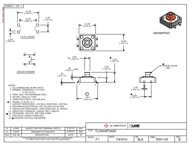
TL3300AF260Q;中文规格书,Datasheet资料
- 格式:pdf
- 大小:121.49 KB
- 文档页数:2
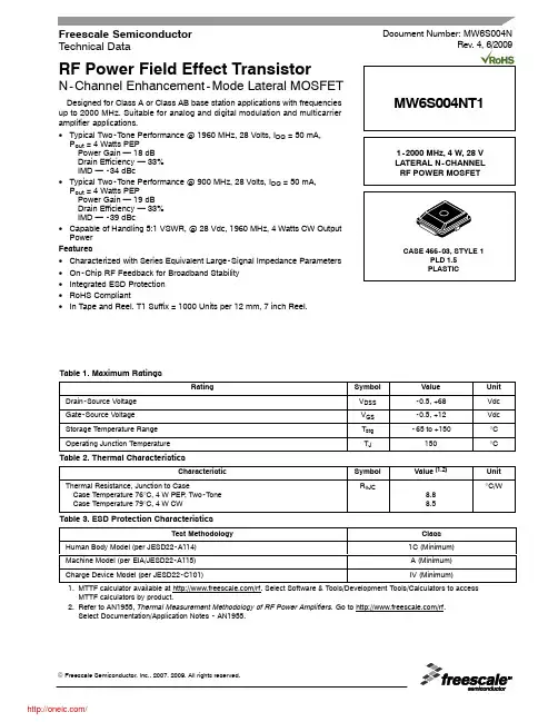
RF Power Field Effect TransistorN-Channel Enhancement-Mode Lateral MOSFETDesigned for Class A or Class AB base station applications with frequencies up to 2000 MHz. Suitable for analog and digital modulation and multicarrier amplifier applications.•Typical Two-Tone Performance @ 1960 MHz, 28 Volts, I DQ = 50 mA, P out = 4 Watts PEP Power Gain — 18 dB Drain Efficiency — 33%IMD — -34 dBc•Typical Two-Tone Performance @ 900 MHz, 28 Volts, I DQ = 50 mA, P out = 4 Watts PEP Power Gain — 19 dB Drain Efficiency — 33%IMD — -39 dBc•Capable of Handling 5:1 VSWR, @ 28 Vdc, 1960 MHz, 4 Watts CW Output Power Features•Characterized with Series Equivalent Large-Signal Impedance Parameters •On-Chip RF Feedback for Broadband Stability •Integrated ESD Protection •RoHS Compliant•In Tape and Reel. T1 Suffix = 1000 Units per 12 mm, 7 inch Reel.Table 1. Maximum RatingsRatingSymbol Value Unit Drain-Source Voltage V DSS -0.5, +68Vdc Gate-Source Voltage V GS -0.5, +12Vdc Storage Temperature Range T stg -65 to +150°C Operating Junction TemperatureT J150°CTable 2. Thermal CharacteristicsCharacteristicSymbol Value (1,2)Unit Thermal Resistance, Junction to CaseCase Temperature 76°C, 4 W PEP , Two-Tone Case Temperature 79°C, 4 W CWR θJC8.88.5°C/WTable 3. ESD Protection CharacteristicsTest MethodologyClass Human Body Model (per JESD22-A114)1C (Minimum)Machine Model (per EIA/JESD22-A115) A (Minimum)Charge Device Model (per JESD22-C101)IV (Minimum)1.MTTF calculator available at /rf. Select Software & Tools/Development Tools/Calculators to access MTTF calculators by product.2.Refer to AN1955, Thermal Measurement Methodology of RF Power Amplifiers. Go to /rf. Select Documentation/Application Notes - AN1955.Document Number: MW6S004NRev. 4, 6/2009Freescale Semiconductor Technical DataMW6S004NT1Table 4. Moisture Sensitivity LevelTest MethodologyRating Package Peak TemperatureUnit Per JESD 22-A113, IPC/JEDEC J-STD-0203260°CTable 5. Electrical Characteristics (T A = 25°C unless otherwise noted)CharacteristicSymbolMinTypMaxUnitOff CharacteristicsZero Gate Voltage Drain Leakage Current (V DS = 68 Vdc, V GS = 0 Vdc)I DSS ——10μAdc Zero Gate Voltage Drain Leakage Current (V DS = 28 Vdc, V GS = 0 Vdc)I DSS ——10μAdc Gate-Source Leakage Current (V GS = 5 Vdc, V DS = 0 Vdc)I GSS——500nAdcOn CharacteristicsGate Threshold Voltage(V DS = 10 Vdc, I D = 50 mAdc)V GS(th) 1.22 2.7Vdc Gate Quiescent Voltage(V DS = 28 Vdc, I D = 50 mAdc)V GS(Q)— 2.7—Vdc Fixture Gate Quiescent Voltage (1)(V DD = 28 Vdc, I D = 50 mAdc, Measured in Functional Test)V GG(Q) 2.23 4.2Vdc Drain-Source On-Voltage(V GS = 10 Vdc, I D = 50 mAdc)V DS(on)—0.270.37VdcDynamic CharacteristicsReverse Transfer Capacitance(V DS = 28 Vdc ± 30 mV(rms)ac @ 1 MHz, V GS = 0 Vdc)C rss —21—pF Output Capacitance(V DS = 28 Vdc ± 30 mV(rms)ac @ 1 MHz, V GS = 0 Vdc)C oss —25—pF Input Capacitance(V DS = 28 Vdc, V GS = 0 Vdc ± 30 mV(rms)ac @ 1 MHz)C iss—30—pFFunctional Tests (In Freescale Test Fixture, 50 ohm system) V DD = 28 Vdc, I DQ = 50 mA, P out = 4 W PEP , f1 = 1960 MHz, f2 = 1960.1 MHz, Two-Tone Test Power Gain G ps 16.51820dB Drain EfficiencyηD 2833—%Intermodulation Distortion IMD —-34-28dBc Input Return LossIRL—-12-10dBTypical Performance (In Freescale 900 MHz Demo Board, 50 ohm system) V DD = 28 Vdc, I DQ = 50 mA, P out = 4 W PEP , f = 900 MHz, Two-Tone Test, 100 kHz Tone Spacing Power Gain G ps —19—dB Drain EfficiencyηD —33—%Intermodulation Distortion IMD —-39—dBc Input Return LossIRL—-12—dB1.V GG = 11/10 x V GS(Q). Parameter measured on Freescale Test Fixture, due to resistive divider network on the board. Refer to Test Circuit Schematic.MW6S004NT1Figure 1. MW6S004NT1 Test Circuit SchematicZ70.210″ x 1.220″ Microstrip Z80.054″ x 0.680″ Microstrip Z90.054″ x 0.260″ Microstrip Z100.025″ x 0.930″ MicrostripPCBArlon CuClad 250GX-0300-55-22, 0.020″, εr = 2.5Z10.054″ x 0.430″ Microstrip Z20.054″ x 0.137″ Microstrip Z30.580″ x 0.420″ Microstrip Z40.580″ x 0.100″ Microstrip Z50.025″ x 0.680″ Microstrip Z60.210″ x 0.100″ MicrostripV SUPPLYTable 6. MW6S004NT1 Test Circuit Component Designations and ValuesPartDescriptionPart Number Manufacturer C1100 nF Chip Capacitor CDR33BX104AKYS Kemet C2, C3, C6, C79.1 pF Chip Capacitors ATC100B9R1CT500XT ATC C4, C510 μF, 50 V Chip Capacitors GRM55DR61H106KA88B Murata C810 μF, 35 V Tantalum Chip Capacitor T490D106K035AT Kemet R1 1 k Ω, 1/4 W Chip Resistor CRCW12061001FKEA Vishay R210 k Ω, 1/4 W Chip Resistor CRCW12061002FKEA Vishay R310 Ω, 1/4 W Chip ResistorCRCW120610R0FKEAVishayMW6S004NT1Figure 2. MW6S004NT1 Test Circuit Component LayoutMW6S004NT1TYPICAL CHARACTERISTICS1420191716G p s , P O W E R G A I N (d B )100.1TWO−TONE SPACING (MHz)1100Figure 6. Intermodulation Distortion Productsversus Tone Spacing 26P in , INPUT POWER (dBm)1618222414Figure 7. Pulsed CW Output Power versusInput PowerI M D , I N T E R M O D U L A T I O N D I S T O R T I O N (d B c )181520MW6S004NT1TYPICAL CHARACTERISTICSA C P R (dB )−70P out , OUTPUT POWER (WATTS) AVG.50−2040−3030−4020−5010−600.01110Figure 8. Single-Carrier CDMA ACPR, Power Gainand Drain Efficiency versus Output PowerP out , OUTPUT POWER (WATTS) CWFigure 10. Power Gain versus Output Power 7151906171618234G p s , P O W E R G A I N (d B )1800−250f, FREQUENCY (MHz)Figure 11. Broadband Frequency Response−5−10−15−20210020502000195019001850S 11 (d B )851ηD , D R A I N E F F I C I E N C Y (%), G p s , P O W E R G A I N (d B )0.118.517.516.515.5MW6S004NT1TYPICAL CHARACTERISTICS25010790T J , JUNCTION TEMPERATURE (°C)Figure 12. MTTF versus Junction TemperatureThis above graph displays calculated MTTF in hours when the device is operated at V DD = 28 Vdc, P out = 4 W PEP, and ηD = 33%.MTTF calculator available at /rf. Select Software & Tools/Development Tools/Calculators to access MTTF calculators by product.106105104110130150170190M T T F (H O U R S )210230MW6S004NT1f = 1930 MHzZ o = 10 ΩZ loadZ sourcef = 1990 MHzf = 1930 MHzf = 1990 MHzV DD = 28 Vdc, I DQ = 50 mA, P out = 4 W PEPfMHzZ sourceWZ loadW1930 1.96 - j5.348.78 + j6.961960 1.89 - j5.108.93 + j7.461990 1.82 - j4.859.11 + j7.97Z source=Test circuit impedance as measured fromgate to ground.Z load=Test circuit impedance as measured fromdrain to ground.Z source Z loadOutputMatchingNetworkFigure 13. Series Equivalent Source and Load ImpedanceMW6S004NT1Table 7. Common Source Scattering Parameters (V DD = 28 V, 50 ohm system)I DQ = 50 mAf MH S 11S 21S 12S 22MHz |S 11|∠φ|S 21|∠φ|S 12|∠φ|S 22|∠φ5000.649-116.3407.902105.4200.056-73.7500.548-33.5705500.695-121.6807.50298.7900.053-80.5700.593-41.4806000.733-126.5607.11192.3800.049-87.0100.632-48.8906500.770-131.340 6.69986.2900.045-93.2800.669-56.0007000.800-135.740 6.30280.4500.041-99.1200.701-62.8107500.827-140.030 5.92274.8500.038-104.8500.727-69.2908000.848-143.950 5.55269.6300.035-110.1100.750-75.3508500.866-147.690 5.22064.5800.032-115.2200.770-81.1309000.882-151.140 4.89159.9700.029-119.9600.786-86.5709500.895-154.560 4.59755.4900.026-124.7900.800-91.73010000.907-157.590 4.31551.2400.024-129.0900.813-96.66010500.916-160.540 4.06047.1700.022-133.3700.824-101.34011000.923-163.310 3.81943.3400.020-137.4600.833-105.79011500.929-165.930 3.60139.6500.018-141.4400.840-110.05012000.935-168.430 3.39836.1100.017-145.3300.847-114.17012500.938-170.770 3.21032.7400.015-149.5400.851-118.06013000.942-173.030 3.03629.4900.014-153.4300.856-121.88013500.945-175.140 2.87526.3600.013-157.4600.859-125.52014000.948-177.170 2.72823.3300.012-161.9100.863-129.02014500.951-179.090 2.59020.4400.011-166.1800.866-132.39015000.953179.030 2.46417.6400.010-170.6300.869-135.65015500.954177.270 2.34714.9200.009-174.8900.872-138.76016000.955175.570 2.24012.3200.008179.9500.875-141.75016500.956173.980 2.1399.7400.008173.9200.877-144.65017000.957172.350 2.0477.2500.007167.7100.880-147.48017500.957170.800 1.958 4.8100.007161.8100.882-150.18018000.958169.340 1.879 2.4400.006155.3700.884-152.76018500.959167.920 1.8060.2600.006148.9400.886-155.23019000.959166.510 1.736-1.9800.005142.6300.887-157.58019500.960165.200 1.668-4.3100.005136.7400.888-160.05020000.959163.800 1.611-6.2400.005129.9100.890-162.07020500.959162.420 1.555-8.2900.005123.8100.891-164.19021000.958161.170 1.504-10.2700.005118.2000.892-166.14021500.958159.840 1.456-12.2100.005112.7400.893-168.06022000.957158.560 1.412-14.1300.005108.4600.894-169.84022500.957157.160 1.372-16.0100.005103.8400.896-171.61023000.955155.870 1.334-17.8700.00599.3100.896-173.26023500.954154.510 1.300-19.7000.00595.3600.897-174.83024000.953153.120 1.268-21.5100.00591.0300.898-176.39024500.953151.7301.238-23.2500.00587.4600.899-177.840MW6S004NT1Table 7. Common Source Scattering Parameters (V DD = 28 V, 50 ohm system) (continued)I DQ = 50 mAf MH S 11S 21S 12S 22MHz |S 11|∠φ|S 21|∠φ|S 12|∠φ|S 22|∠φ25000.952150.340 1.211-25.1200.00684.1600.899-179.27025500.950149.010 1.187-26.9200.00680.7800.897179.42026000.949147.380 1.166-28.6500.00677.8800.897178.12026500.948145.920 1.144-30.4200.00774.6700.898176.84027000.944144.200 1.121-32.3100.00771.3600.896175.48027500.944142.790 1.105-34.2300.00767.9800.897174.06028000.943141.020 1.088-36.0000.00763.9500.897172.93028500.941139.410 1.073-37.8700.00761.2300.896171.63029000.940137.640 1.058-39.7600.00859.8100.896170.33029500.938135.900 1.045-41.6800.00858.2800.896169.04030000.937133.8601.032-43.6100.00856.7400.895167.510分销商库存信息: FREESCALEMW6S004NT1。
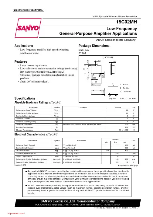

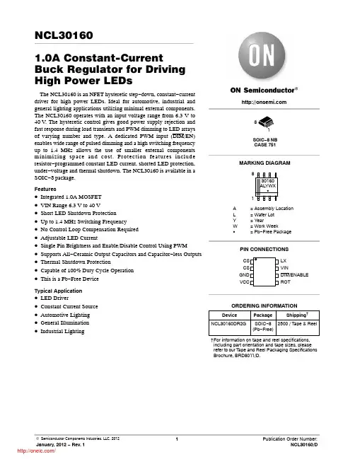
NCL301601.0A Constant-CurrentBuck Regulator for Driving High Power LEDsThe NCL30160 is an NFET hysteretic step−down, constant−current driver for high power LEDs. Ideal for automotive, industrial and general lighting applications utilizing minimal external components. The NCL30160 operates with an input voltage range from 6.3 V to 40 V. The hysteretic control gives good power supply rejection and fast response during load transients and PWM dimming to LED arrays of varying number and type. A dedicated PWM input (DIM/EN) enables wide range of pulsed dimming and a high switching frequency up to 1.4 MHz allows the use of smaller external components minimizing space and cost. Protection features include resistor−programmed constant LED current, shorted LED protection, under−voltage and thermal shutdown. The NCL30160 is available in a SOIC−8 package.Features•Integrated 1.0A MOSFET•VIN Range 6.3 V to 40 V•Short LED Shutdown Protection•Up to 1.4 MHz Switching Frequency•No Control Loop Compensation Required•Adjustable LED Current•Single Pin Brightness and Enable/Disable Control Using PWM •Supports All−Ceramic Output Capacitors and Capacitor−less Outputs •Thermal Shutdown Protection•Capable of 100% Duty Cycle Operation•This is a Pb−Free DeviceTypical Application•LED Driver•Constant Current Source•Automotive Lighting•General Illumination•Industrial LightingDevice Package Shipping†ORDERING INFORMATIONNCL30160DR2G SOIC−8(Pb−Free)2500 / Tape & Reel†For information on tape and reel specifications, including part orientation and tape sizes, please refer to our T ape and Reel Packaging Specifications Brochure, BRD8011/D.SOIC−8 NBCASE 751MARKING DIAGRAMA= Assembly LocationL= Wafer LotY= YearW= Work WeekG= Pb−Free Package8PIN CONNECTIONSCSCSGNDVCCLXVINROTDIM/ENABLEFigure 1. Typical Application CircuitD1SENSEPIN FUNCTION DESCRIPTIONPin Pin NameDescriptionApplication Information1, 2CS Current Sense feedback pinSet the current through the LED array by connecting a resistor from this pin to ground.3GND Ground PinGround. Reference point for all voltages4VCCOutput of Internal 5 V linearregulatorThe VCC pin supplies the power to the internal circuitry. The VCC is the output of a linear regulator which is powered from VIN. A 2 uF ceramiccapacitor is recommended for bypassing and should be placed as close as possible to the VCC and AGND pins. Do not connect to an external load.5R OT Off −Time Setting Resistor Resistor ROT from this pin to VCC sets the Off −Time range for the hysteretic controller.6DIM/EN PWM Dimming Control &ENABLEConnect a logic −level PWM signal to this pin to enable/disable the power MOSFET and LED array7VINInput Voltage PinNominal operating input range is 6.3 V to 40 V. Input supply pin to the internal circuitry and the positive input to the current sense comparators. Due high frequency noise, a 10 m F ceramic capacitor is recommended to be placed as close as possible to VIN and power ground.8LXDrain of Internal PowerMOSFETThe LX pin connects to the inductor and provides the switching current necessary to operate in hysteretic mode.MAXIMUM RATINGSRating Symbol Min Max Unit VIN to GND VIN−0.340V MOSFET Drain Voltage to GND LX−40V VCC to GND VCC−6V DIM/EN to GND DIM−0.36V CS to GND CS−0.36V ROT to GND ROT−0.36V Absolute Maximum Junction Temperature T J(MAX)150°C Operating Junction Temperature Range T J−40125°C Maximum LED Drive Current ILIM 1.5A Storage Temperature Range T stg−55 to +125°C Thermal CharacteristicsSOIC−8 Plastic Package Maximum Power Dissipation @ T A = 25°C (Note 1) Thermal Resistance Junction−to−Air (Note 2)PDR q JA1.11111.7W°C/WLead Temperature Soldering (10 sec):Re−flow (SMD styles only) Pb−Free (Note 3)T L260 peak°C Moisture Sensitivity Level (Note 4)MSL1−Stresses exceeding Maximum Ratings may damage the device. Maximum Ratings are stress ratings only. Functional operation above the Recommended Operating Conditions is not implied. Extended exposure to stresses above the Recommended Operating Conditions may affect device reliability.1.The maximum package power dissipation limit must not be exceeded.P D+T J(max)*T AR q JA2.When mounted on a multi−layer board with 35 mm2 copper area, using 1 oz Cu.3.60−180 seconds minimum above 237°C.4.Moisture Sensitivity Level (MSL): 1 per IPC/JEDEC standard: J−STD−020A.ELECTRICAL CHARACTERISTICS (Unless otherwise noted: V IN = 12 V, T A = 25°C, unless otherwise specified.)Symbol Characteristics Min Typ Max Unit SYSTEM PARAMETERSV IN Input Supply Voltage Range Normal Operation8.040VFunctional (Note 5) 6.3I Q_IN Quiescent Current into V IN 1.5mAV CC Internal Regulator Output (Note 6) 5.0V V UV+Under−Voltage Lock−out Threshold(V IN Rising)5.56.0 6.5 VV UV−Under−Voltage Lock−out Threshold(V IN Falling)5.2 5.66.3 V CURRENT LIMIT AND REGULATIONV CS_UL CS Regulation Upper Limit(CS Increasing, FET Turns−OFF)25°C213220226mV −40 to 125°C209231V CS_LL CS Regulation Lower Limit(CS Decreasing, FET Turns−ON)25°C174180186mV −40 to 125°C171189V OCP Over Current Protect Limit(Reference to CS Pin)500mVF SW Switching Frequency Range (Note 7)1400kHz DIM INPUTV PWMH/L PWM (DIM/EN) high level input voltage 1.4V V PWML PWM (DIM/EN) low level input voltage0.4VI DIM−PU DIM/EN Pull−up Current50m Af pwm PWM (DIM/EN) dimming frequency range0.120kHzdmax Maximum Duty Cycle (Note 7)100% POWER MOSFETV BRDSS Drain−to−Source Breakdown Voltage40VI DSS Drain−to−Source Leakage Current(V GS = 0 V, V DS = 40 V)10m AR DS(on)On Resistance(Id = 500 mA)55m WV SD Source−Drain Body Diode(Forward On−Voltage)0.8 1.1Vt PD_Off Propagation Delay V CS_UL− LX_High35ns THERMAL SHUTDOWNT SD Thermal Shutdown165 °C T Hyst Thermal Hysteresis40°C OFF TIMERt OFF−MIN Minimum Off−time137ns 5.The functional range of V IN is the voltage range over which the device will function. Output current and internal parameters may deviate fromnormal values for V IN and V CC voltages between 6.3 V and 8 V, depending on load conditions6.V CC should not be driven from a voltage higher than V IN or in the absence of a voltage at V IN.7.Guaranteed by design.Figure 2. Simplified Block DiagramLXCSVCCROTDIM / EnableGNDTYPICAL APPLICATION CIRCUITS AND WAVEFORMS(T J = 25°C, Unless Otherwise Specified)Figure 3. Typical Application Circuit To Drive One LED (Buck)D1SENSEFigure 4. Typical Operation Waveforms(V CC = 12 V, V LED = 6.5 V, R SENSE = 0.68 W , L = 100 mH)THEORY OF OPERATIONThis switching power supply is comprised of an inverted buck regulator controlled by a current mode, hysteretic control circuit. The buck regulator operates exactly like a conventional buck regulator except the power device placement has been inverted to allow for a low side power FET. Referring to Figure 1, when the FET is conducting,current flows from the input,through the inductor, the LED and the FET to ground.When the FET shuts off, current continues to flow through the inductor and LED, but is diverted through the diode (D1). This operation keeps the current in the LED continuous with a continuous current ramp.The control circuit controls the current hysteretically.Figure 2 illustrates the operation of this circuit. The CS comparator thresholds are set to provide a 10% current ripple. The peak current comparator threshold of 220 mV sets I peak at 10% above the average current while the valley current comparator threshold of 180 mV sets I valley at 10%below the average current.When the FET is conducting, the current in the inductor ramps up. This current is sensed by an external sense resistor that is connected from CS to ground. When the CS pin reaches 220 mV , the peak current comparator turns off the power FET. A conventional hysteretic controller would monitor the load current and turn the switch back on when the CS pin reaches 180 mV . But in this topology, the current information is not available to the control circuit when the FET is off. To set the proper FET off time, the CS voltage issensed when the FET is turned back on and a correction signal is sent to the off time circuit to adjust the off time asnecessary.Figure 5. Typical Current WaveformsThe current waveshape is triangular, and the peak and valley currents are controlled. The average value for a triangular waveshape is halfway between the peak and valley, so even with changes in duty cycle due to input voltage variations or load changes, the average current will remain constant.In the event there is a short −circuit across the LEDs, a large amount of current could potentially flow through the circuit during startup. To protect against this, the NCL30160comes with a short circuit protection feature. If the voltage on the CS pin is detected to be greater than 500 mV (equating to 2.5 times the intended average output current),the NCL31060 will turn off the FET, and prevent the FET from turning on again until power is recycled to NCL30160.Figure 6. Short-Circuit ProtectionWhen V IN rises above the UVLO threshold voltage, switching operation of the FET will begin. However, until the V IN voltage reaches 8 V, the VCC regulator may not provide the expected gate drive voltage to the FET. This could result in the R DS(on) of the FET being higher than expected or there not being enough gate drive capability to operate at the maximum rated switching frequency. For optimal performance, it is recommended to operate the part at a V IN voltage of 8 V or greater.Setting The Output CurrentThe average output current is determined as being the middle of the peak and valley of the output current, set by the CS comparator thresholds. The nominal average output current will be the current value equivalent to 200 mV at the CS pin. The proper R SENSE value for a desired average output current can be calculated by:R SENSE+200mV I LEDPWM DimmingFor a given R SENSE value, the average output current, and therefore the brightness of the LED, can be set to a lower value through the DIM/EN pin. When the DIM/EN pin is brought low, the internal FET will turn off and switching will remain off until the DIM/EN pin is brought back into its high state.Figure 7. Dimming WaveformsBy applying a pulsed signal to DIM/EN, the average output current can be adjusted to the duty ratio of the pulsed signal. It is recommended to keep the frequency of the DIM/EN signal above 100 Hz to avoid any visible flickering of the LED.Figure 8. Dimming PerformanceInductor SelectionThe inductor that is used directly affects the switching frequency the driver operates at. The value of the inductor sets the slope at which the output current rises and falls during the switching operation. The slope of the current, in turn, determines how long it takes the current to go from the valley point of the current ripple to the peak when the FET is on and the current and rising, and how long it takes the current to go from the peak point of the current to the valley when the FET is off and the current is falling. These times can be approximated from the following equations:+L D IVIN*V LED*I OUTǒFET R DS(on))DCR L)R SENSEǓt ONt OFF+L D IV LED)V diode)I OUT DCR LWhere DCR L is the dc resistance of the inductor, V LED is the forward voltages of the LEDs, FET RDS(ON) is the on-resistance of the power MOSFET, and V diode is the forward voltage of the catch diode.The switching frequency can then be approximated from the following:f SW+1t ON)t OFFHigher values of inductance lead to slower rates of rise and fall of the output current. This allows for smaller discrepancies between the expected and actual output current ripple due to propagation delays between sensing at the CS pin and the turning on and off of the power MOSFET. However, the inductor value should be chosen such that the peak output current value does not exceed the rated saturation current of the inductor.Catch Diode SelectionThe catch diode needs to be selected such that average current through the diode does not exceed the rated average forward current of the diode. The average current through the diode can be calculated as:I avg_diode+I OUTt OFFt ON)t OFFIt is also important to select a diode that is capable ofwithstanding the peak reverse voltage it will see in theapplication. It is recommended to select a diode with a ratedreverse voltage greater than VIN. It is also recommended touse a low-capacitance Schottky diode for better efficiencyperformance.Selecting The Off-Time Setting ResistorThe off-time setting resistor (R OT) programs theNCL30160 with the initial time duration that the MOSFETis turned off when the switching operation begins. Duringsubsequent switching cycles, the voltage at the CS pin issensed every time the MOSFET is turned on, and theoff-time will be adjusted depending on how much of adiscrepancy exists between the sensed value and the CSlower limit threshold value. The R OT value can be calculatedusing the following equation:R OT+t OFF1011WWhere t OFF is the expected off time during normalswitching operation, calculated in the Inductor Selectionsection above.Input CapacitorA decoupling capacitor from VIN to ground should beused to provide the current needed when the powerMOSFET turns on. A 4.7 m F ceramic capacitor isrecommended.Figure 9. Efficiency, 350 mA, V f_LED = 3.5 VFigure 10. Efficiency, 700 mA, V f_LED = 3.5 VFigure 11. Efficiency, 1 A, V f_LED = 3.5 VFigure 12. IQIN vs. VINFigure 13. LED Current vs. Dimming DutyRatio10095908580757065600510152025303540VIN (V)E F F I C I E N C Y (%)10095908580757065600510152025303540VIN (V)E F F I C I E N C Y (%)10095908580757065600510152025303540VIN (V)E F F I C I E N C Y (%)1.701.651.601.551.501.451.401.351.30VIN (V)I Q I N (m A )DIMMING DUTY RATIO (%)L E D C U R R E N T (m A )−40−2020406080100120240220200180160140120100S W I T C H I N G F R E Q U E N C Y (k H z )Figure 14. Switching Frequency vs.Temperature (12 V V IN , 3 LEDs, 0.7 A, 0.47 m H)TEMPERATURE (°C)PACKAGE DIMENSIONSSOIC −8 NB CASE 751−07ISSUE AKNOTES:1.DIMENSIONING AND TOLERANCING PER ANSI Y14.5M, 1982.2.CONTROLLING DIMENSION: MILLIMETER.3.DIMENSION A AND B DO NOT INCLUDE MOLD PROTRUSION.4.MAXIMUM MOLD PROTRUSION 0.15 (0.006)PER SIDE.5.DIMENSION D DOES NOT INCLUDE DAMBAR PROTRUSION. ALLOWABLE DAMBARPROTRUSION SHALL BE 0.127 (0.005) TOTAL IN EXCESS OF THE D DIMENSION AT MAXIMUM MATERIAL CONDITION.6.751−01 THRU 751−06 ARE OBSOLETE. NEW STANDARD IS 751−07.DIM A MIN MAX MIN MAX INCHES4.805.000.1890.197MILLIMETERS B 3.80 4.000.1500.157C 1.35 1.750.0530.069D 0.330.510.0130.020G 1.27 BSC 0.050 BSC H 0.100.250.0040.010J 0.190.250.0070.010K 0.40 1.270.0160.050M 0 8 0 8 N 0.250.500.0100.020S5.806.200.2280.244MYM0.25 (0.010)YM0.25 (0.010)Z SXS____0.60.024ǒmm inchesǓSCALE 6:1*For additional information on our Pb −Free strategy and solderingdetails, please download the ON Semiconductor Soldering and Mounting Techniques Reference Manual, SOLDERRM/D.SOLDERING FOOTPRINT*ON Semiconductor and are registered trademarks of Semiconductor Components Industries, LLC (SCILLC). SCILLC reserves the right to make changes without further notice to any products herein. SCILLC makes no warranty, representation or guarantee regarding the suitability of its products for any particular purpose, nor does SCILLC assume any liability arising out of the application or use of any product or circuit, and specifically disclaims any and all liability, including without limitation special, consequential or incidental damages.“Typical” parameters which may be provided in SCILLC data sheets and/or specifications can and do vary in different applications and actual performance may vary over time. All operating parameters, including “Typicals” must be validated for each customer application by customer’s technical experts. SCILLC does not convey any license under its patent rights nor the rights of others. SCILLC products are not designed, intended, or authorized for use as components in systems intended for surgical implant into the body, or other applications intended to support or sustain life, or for any other application in which the failure of the SCILLC product could create a situation where personal injury or death may occur. Should Buyer purchase or use SCILLC products for any such unintended or unauthorized application, Buyer shall indemnify and hold SCILLC and its officers, employees, subsidiaries, affiliates,and distributors harmless against all claims, costs, damages, and expenses, and reasonable attorney fees arising out of, directly or indirectly, any claim of personal injury or death associated with such unintended or unauthorized use, even if such claim alleges that SCILLC was negligent regarding the design or manufacture of the part. SCILLC is an Equal Opportunity/Affirmative Action Employer. This literature is subject to all applicable copyright laws and is not for resale in any manner.PUBLICATION ORDERING INFORMATION分销商库存信息: ONSEMINCL30160DR2G。