国债逆回购操作全攻略:月末季末收益可达10%divdiv
- 格式:docx
- 大小:13.48 KB
- 文档页数:6


AS-1H1V-WP Technical SpecificationsThe Intelix AS-1H1V-WP is a two-gang, Decora-style wallplate designed to be the primary PC interface for classrooms, boardrooms, and conference centers. It features VGA + Audio to HDMI conversion with VGA scaling up to 1920x1200 and an HDMI input.The AS-1H1V-WP utilizes HDBaseT technology to extend the digital output up to 70 meters away using solid core shielded Category 5e or greater cable. This transmitter device is compatible with several Intelix HDBaseT receivers, but is designed to work primarily with the DIGI-HD60C-R. The unit features multiple EDID modes to eliminate user confusion, and incompatible video formats.The AS-1H1V can be powered from the rear panel or by Power over HDBaseT (PoH), including midspan injectors that support Power over Ethernet (PoE) Alternative A or Alternative B. Built-in surge protection and diagnostic LEDs ensure hassle-free and robust installations. The AS-1H1V-WP also features a customizable power management system, which will put the unit into a low power state after no video for 30 minutes or being inactive for 3 hours by default. When using the local power input, 12V DC is available for other devices on the power output connections on the rear of the device.The AS-1H1V-WP will detect which input has an active video input, and switch to that input – if both inputs are active, the “last in” will be selected. There are additional contact closure inputs provided on the rear of the unit to allow third party control. RS232 control of the AS-1H1V-WP can be accomplished by connecting to the RS232 port on a compatible receiver, such as a DIGI-HD60C-R, or through a direct connection on the RS232 input of the device.The AS-1H1V-WP can be programmed to control the connected display. The display manufacturer’s RS232 commands can be entered into the AS-1H1V-WP with the use of Intelix Display Control software. This allows display power and input to be automatically controlled based on video activity, eliminating the need for a third party control system in many installations.AS-1H1V-WP Technical SpecificationsHDMI and VGA Auto-Switching WallplateRev 160804AS-1H1V-WP Technical SpecificationsAS-1H1V-WP Technical Specifications Input/Output ConnectionsHDMI Input One (1) HDMI Type A ReceptacleVGA Input One (1) PC Video HD-15-F ReceptacleAnalog Audio One (1) 3.5 mm TRS ReceptacleHDBaseT Port One (1) 8P8C port (Shielded RJ45)Power One (1) 2-pin Removable Terminal Block ConnectorRS232 Port with 12V DC Output One (1) 4-pin Removable Terminal Block ConnectorContact Closures One (1) 4-pin Removable Terminal Block ConnectorFirmware Port One (1) USB Type B Micro ReceptacleSupported Audio, Video and ControlVideo Resolutions SMPTE: 480i, 480p, 576i, 576p, 720p, 1080i, 1080p, UHD/30 (HDMI only)VESA: Resolutions up to 1920x1200Color Depth: 24, 30, 36, 48bitVGA Scaling Resolutions (60 Hz)1024x768, 1400x1050, 1600x1200, 1280x800, 1360x768, 1920x1200, 720p, 1080pMaximum Video Compatibility at 70 m Deep Color 36/30/24 Bit at 1080pMaximum Video Compatibility at 40 m Deep Color 48 Bit at 1080p, 3D (HDMI Input), UHD/30Video Compliance HDMI 1.4 and HDCP 1.4Embedded Audio Up to PCM 8 channel, Dolby Digital TrueHD, and DTS-HD Master AudioAnalog Audio Analog stereo line-level (Converted to 2ch 24bit PCM 48kHz)ARC (Audio Return Channel)NoHEC (HDMI Ethernet Channel)NoCEC (Consumer Electronics Control)Yes (HDMI Pass-through Only)Baud Rate (Wall plate control)2400, 4800, 9600 (default), 19200, 38400, 57600, 115200Supported Baud Rates (Display Control)2400, 4800, 9600, 19200, 38400, 57600, 115200HDBaseT Signal CharacteristicsMaximum Distance70 m (229 ft)Cable Requirements Continuous solid core Category 5e or greater with TIA/EIA-568B crimp pattern (no couplers in-line)Bandwidth10.2 GbpsHDBaseT Chipset VS010TXChassis and EnvironmentalConstruction Alumininum HousingDimensions (H x W x D)104 mm x 89 mm x 51 mm (4.09 in x 3.50 in x 2.01 in)Shipping Weight0.68 kg (11.5 lbs.)Operating Temperature0° to +40° C (+32° to +104° F)Operating Humidity20% to 90%, Non-condensingStorage Temperature-10° to +60° C (+14° to +140° F)Storage Humidity20% to 90%, Non-condensingPower and RegulatoryPower Supply12V DC 2A or 48V DC PoH (Power over HDBaseT)Power Output Port12V DC, 500 mAPower over Ethernet (PoE) Compatibility802.3af Alternative A and Alternative BPower Consumption10 wattsDefault Automatic Standby Mode30 minutes no signalESD Protection16kVRegulatory CE, RoHSOtherWarranty 2 yearsDiagnostic Indicators HDCP, Link, VGA, and HDMIReset Switch MicroswitchAvailable Models AS-1H1V-WP-W (White Faceplate and Painted Insert), AS-1H1V-WP-B (Black Faceplate and Painted Insert) Included Accessories Installation Guide, Power Supply, Two (2) 4-pin Removable Screw Terminals, RS232 cable (3-pin to DE9), 2-pinRemovable Screw Terminal, USB Programming CableHDBaseT Receiver (A/V, PoE, Control) Compatibility DIGI-HD60C-R, DIGI-HDX-R, FLX-64, DIGI-BSR-4KHDBaseT Receiver (A/V, Control) Compatibility FLX-BI4HDBaseT Receiver (A/V and PoE) Compatibility DIGI-HD60-RDistances and picture quality may be affected by cable grade, cable quality, source and destination equipment, RF and electrical interference, and cable patches.。

Board Specification Tesla C1060 Computing ProcessorBoardDocument Change HistoryVersion Date Responsible Description of Change01 July 10, 2008 SG, SM Preliminary Release02 July 15, 2008 SG, SM Minor text updatesUpdated Support Information section 03 September 22, 2008 SG, SM Initial ReleaseUpdated thermal informationMinor text updates04 December 8, 2008 SG, SM Updated fan flow and power information05 January 22, 2009 SG, SM Updated board powerTable of ContentsTesla C1060 Overview (1)Key Features (1)Computing Processor Description (2)Configuration (3)Mechanical Specifications (4)PCI Express System (4)Standard I/O Connector Placement (5)Internal Connectors and Headers (6)External PCI Express Power Connectors (6)4-Pin Fan Connector (9)Power Specifications (11)Power by Rail (12)Thermal Specifications (13)Thermal Qualification Summary (13)Cooling Solution (15)Support Information (17)Languages (17)Certificates and Agencies (18)Agencies (18)List of FiguresFigure 1. Tesla C1060 Block Diagram (2)Figure 2. Tesla C1060 Computing Processor Board (4)Figure 3. Tesla C1060 Bracket (No Connectors) (5)Figure 4. 6-Pin PCI Express Power Connector (7)Figure 5. 8-Pin PCI Express Power Connector (8)Figure 6. 4-Pin Fan Connector (10)Figure 7. TM72 Active Fan Sink (15)List of TablesTable 1. Board Configuration (3)Table 2. 6-Pin PCI Express Power Connector Pinout (9)Table 3. 8-Pin PCI Express Power Connector Pinout (9)Table 4. 4 Wire Thermal Control Pinout (10)Table 5. Configuration with External PCI Express Connectors (11)Table 6. Power by Rail (12)Table 7. Test Setup and Configuration (14)Table 8. Sample Thermal Results and Specification (14)Table 9. Fan Specifications and Conditions (16)Table 10. Environmental Specifications and Conditions (16)Table 11. Languages Supported (17)Tesla C1060 Overview The NVIDIA® Tesla™ C1060 computing processor board is a PCI Express 2.0 full-height (4.376 inches by 10.50 inches) form factor computing add-in card based onthe NVIDIA Tesla T10 graphics processing unit (GPU). This board is targeted ashigh-performance computing (HPC) solution for PCI Express systems.The Tesla C1060 is capable of 933 GFLOPs/s of processing performance andcomes standard with 4 GB of GDDR3 memory at 102 GB/s bandwith.Key FeaturesGPUNumber of processor cores: 240Processor core clock: 1.296 GHzVoltage: 1.1875 VPackage size: 45.0 mm × 45.0 mm 2236-pin flip-chip ball grid array (FCBGA)BoardFourteen layer printed circuit board (PCB)PCI Express 2.0 ×16 system interfacePhysical dimensions: 4.376 inches × 10.50 inches, dual slotBoard power dissipation: 187.8 WExternal ConnectorsNoneInternal Connectors and HeadersOne 6-pin PCI Express power connectorOne 8-pin PCI Express power connector4-pin fan connectorMemory800 MHz512-bit memory interface4 GB: Thirty-two pieces 32M × 32 GDDR3 136-pin BGA, SDRAMBIOS1Mbit Serial ROMComputing ProcessorDescriptionFigure 1 is a block diagram of the Tesla C1060 computing processor.Tesla C1060 Computing Processor-Figure 1. Tesla C1060 Block DiagramConfigurationThere is one configuration available (Table 1) for the Tesla C1060 board.Table 1. Board ConfigurationSpecification DescriptionGeneric SKU reference 900-20607-0000-000Chip Tesla T10 GPUPackage size: GPU 45.0 x 45.0 mmProcessor clock 1296 MHzMemory clock 800 MHzMemory size 4 GBMemory I/O 512-bit GDDR3Memory configuration 32 pcs 32M × 32 GDDR3 SDRAMExternal connectors NoneInternal connectors and headers 8-pin PCI Express power connector6-pin PCI Express power connector4-pin fan connectorBoard power 187.8 W (idle power = 57.65 W)Thermal cooling solution TM72 active fan sinkMechanical SpecificationsPCI Express SystemThe Tesla C1060 computing processor board (Figure 2) conforms to the PCI Express full height (4.376 inches by 10.50 inches) form factor.Figure 2. Tesla C1060 Computing Processor Board4.376 inches10.50 inchesStandard I/O ConnectorPlacementAs shown in Figure 3, the Tesla C1060 does not include any external I/Oconnectors.Figure 3. Tesla C1060 Bracket (No Connectors)Internal Connectors andHeadersThe Tesla C1060 board supports the following internal connectors and headers.8-pin PCI Express power connector (can be used with a 6-pin power cable)6-pin PCI Express power connector4-pin fan connectorExternal PCI Express Power ConnectorsThe Tesla C1060 is a performance-optimized, high-end board and utilizes powerfrom the PCI Express connector as well as external power connectors. The boardcan be used in two different ways.One 8-pin PCI Express power connector orTwo 6-pin PCI Express power connectorsNote:When connecting two 6-pin power cables to the two power connectors on theTesla C1060 board, ensure that both power cables come from the same powerrail. For example, the same 12 V power supply.Figure 4 and Figure 5 show the specifications, and Table 2 and Table 3 show thepinouts for the 6-pin and 8-pin external PCI Express power connectors,respectively.Figure 4. 6-Pin PCI Express Power ConnectorFigure 5. 8-Pin PCI Express Power ConnectorTable 2. 6-Pin PCI Express Power Connector PinoutPin Number DescriptionV1 +12V2 +12V3 +124 GND5 Sense6 GNDTable 3. 8-Pin PCI Express Power Connector PinoutPin Number DescriptionV1 +12V2 +12V3 +124 Sense15 GND6 Sense07 GND8 GND4-Pin Fan ConnectorThe Tesla C1060 board uses a 4-pin fan to control the fan speed of the thermalsolution. The details of the connector (P/N: PH-T-4) are given in Figure 6. Thispart is a 2.0 mm (0.079") pitch disconnectable connector.Table 4 lists the pin assignments for this connector.Figure 6. 4-Pin Fan ConnectorTable 4.4 Wire Thermal Control PinoutPin Number Description 1 PWM (to fan) 2TACH (from fan)3 +12 V4 GNDPowerSpecifications The Tesla C1060 computing processor is a performance optimized high-end board solution. Power is taken from the PCI Express host bus as well as either one 8-pin or two 6-pin PCI Express power connectors.Note:When connecting two 6-pin power cables to the two power connectors on the Tesla C1060 board, ensure that both power cables come from the same powerrail. For example, the same 12 V power supply.Without auxiliary power provided to the Tesla C1060 board, the board will not boot and LED lights on the board will light up as listed in Table 5. This table outlines the different possible scenarios as well as the resulting behaviors.Table 5. Configuration with External PCI ExpressConnectors8-pin Power Connector 6-pin PowerConnectorResultConnected(either 8-pin or 6-pin) Connected Full Power – LED light on the bracketis GREEN by default8-pin Connected Not Connected Full Power – LED light on the bracketis GREEN by default6-pin Connected Not Connected LED light is RED – board will not bootto OSNot Connected Connected LED light is RED – board will not bootto OSNot Connected Not Connected LED light is RED – board will not bootTesla C1060 Computing Processor BoardPower by RailTable 6 lists the power by rail numbers for the Tesla C1060 board.Table 6. Power by RailPEX12V PEX3V3 EX12V Total Board PowerW62.01 2.82124.25 187.82 8-pin Connected Not connected Full Power – LED light onthe bracket is GREEN bydefaultThermalSpecificationsThermal Qualification SummaryThe information contained in this summary report is intended to provide users ofthe Tesla C1060 computing processor with thermal information necessary to assistin thermal management efforts. This information is not intended to provide aspecific thermal management solution. However, it does show an approach thatresult in the reliable operation of the Tesla C1060.The product and cooling solutions used are:Device product: Tesla C1060 boardCooling solution: Fan sink solution, Cooler Master TM72 NV P/N: 580-10607-2000-000. The cooling solution assembly includes a heat sink, fan, backplate,thermal grease interface material, and screws.Result: Under the operating conditions described in the following tables, theTesla C1060 passed thermal qualification.Table 7. Test Setup and ConfigurationSystem Part ConfigurationPC Motherboard attached to a chassis frame – entireunit placed in an acrylic boxMotherboard NVIDIAnForce® 790i Ultra SLIPower Supply ThermalTake 1000 WCPU Intel Core 2 Extreme QX9650 Yorkfield 3.0 GHz12 MB L2 Cach LGA 775 130 W Quad-CoreprocessorSDRAM DDR3 1333; 2 – 1 GB OCZ memory cardsPC Operating System Windows XP 32-bitGPU Computing ProcessingBoard Tesla C1060BIOS 62.00.1E.00.00 Display Driver 177.83GPU TeslaT10Clock Speed 1.296 GHz (core) 800 MHz (mclk)Table 8. Sample Thermal Results and SpecificationTest Application Tjunction(°C)* TA(°C)** CoolingSolutionTest 1:3DMark06/GT2Firefly87 45.4GPU junctionmaximumtemperature specification under any operating conditions. 102At anyambientTemperatureFan sink solution,NV P/N 580-10607-2000-000* Junction temperature is reported by NVIDIA thermal sensor** Ambient air temperature – average of 3 sensors positioned at the inlet to the GPU fanCooling SolutionNVIDIA will utilize a CoolerMaster TM72 active fan sink (Figure 7) to cool theGPU, memories and power supply components. For fan and environmentalspecifications refer to Table 9 and Table 10.Figure 7. TM72 Active Fan SinkTable 9. Fan Specifications and ConditionsSpecifications ConditionsRated voltage 12 V DCOperating voltage 5 V ~ 13.2 V DCStart up voltage 5.0 V (at 100% duty cycle at 25 o C power on/off) Rated current 0.48 AmpRated power 5.76 WSpeed 2600±10% RPM (At 25 o C to record speed afterfan running normal. This time is about 3-5minutes)Speed (with customer’s pillow) 2600 RPM ± 10%14.08 CFM (minimum 12.67 CFM)Air flow (at zero static pressurewith customer’s pillow)11.21 mm water (minimum 9.08 mm water)Air pressure (at zero air flow withcustomer’s pillow)Acoustic noise 39.4 dB(A); maximum 43.3 dB(A)Noise (with customer’s pillow) 46.0 dB(A); Max 50.6 dB(A)Life expectance 70,000 hours continuous operation at 40 °C with15 – 65 % relative humidityTable 10. Environmental Specifications and ConditionsSpecifications ConditionsOperating temperature 0 °C to 45 °CStorage temperature All function shall be normal after 500 hours at -10 °Cto 70 °C at normal humidity with a 24 hours recoveryperiod at room temperatureOperating humidity 5% to 90 % RHStorage humidity 5% to 95 % RHJanuary 22, 2009 | BD-04111-001_v0517Support InformationLanguagesTable 11.Languages SupportedWinXPLinuxEnglish (US) x x English (UK) x Arabic xChinese, Simplified x Chinese, TraditionalxDanish x Dutch x Finnish x French x French (Canada)xGerman x Italian x Japanese x Korean x Norwegian x Portuguese (Brazil)xRussian x Spanish x Spanish (Latin America)xSwedish x Thai x NOTE: NVIDIA’s CUDA™ software is only supported in English (U.S.)Tesla C1060 Computing Processor BoardCertificates and AgenciesAgenciesBureau of Standards, Metrology, and Inspection (BSMI)C-TickConformité Européenne (CE)Federal Communications Commission (FCC)Interference-Causing Equipment Standard (ICES)Ministry of Information and Communication (MIC)Underwriters Laboratories (UL)Voluntary Control Council for Interference (VCCI)January 22, 2009 | BD-04111-001_v0518NoticeALL NVIDIA DESIGN SPECIFICATIONS, REFERENCE BOARDS, FILES, DRAWINGS, DIAGNOSTICS, LISTS, ANDOTHER DOCUMENTS (TOGETHER AND SEPARATELY, “MATERIALS”) ARE BEING PROVIDED “AS IS.” NVIDIAMAKES NO WARRANTIES, EXPRESSED, IMPLIED, STATUTORY, OR OTHERWISE WITH RESPECT TO THEMATERIALS, AND EXPRESSLY DISCLAIMS ALL IMPLIED WARRANTIES OF NONINFRINGEMENT,MERCHANTABILITY, AND FITNESS FOR A PARTICULAR PURPOSE.Information furnished is believed to be accurate and reliable. However, NVIDIA Corporation assumes noresponsibility for the consequences of use of such information or for any infringement of patents or otherrights of third parties that may result from its use. No license is granted by implication or otherwise under any patent or patent rights of NVIDIA Corporation. Specifications mentioned in this publication are subject tochange without notice. This publication supersedes and replaces all information previously supplied. NVIDIACorporation products are not authorized for use as critical components in life support devices or systemswithout express written approval of NVIDIA Corporation.TrademarksNVIDIA, the NVIDIA logo, CUDA, HybridPower, nForce, SLI and Tesla are trademarks or registeredtrademarks of NVIDIA Corporation in the United States and other countries. Other company and productnames may be trademarks of the respective companies with which they are associated.Copyright© 2008, 2009 NVIDIA Corporation. All rights reserved.。

Philips Signage Solutions D-Line Display65"UHD (3840 x 2160)500cd/m²65BDL4510DSay moreSmart, fast 24/7 display.Make it stand out with a fast D-Line professional 4K UHD display. Philips’ superb picture quality ensures true colours and intense contrast. You can effortlessly display content from multiple sources on a single screen.Effortless setup. Total control.•Operate, monitor and maintain with CMND & Control •Schedule what you want, when you want with SmartPlayer Cost-effective system solution•FailOver ensures content is always playing •Energy-saving automatic backlight control Brilliant picture. Blazing processor speed.•4K UHD. Rich, deep images. Stunning contrast •ADS wide-view panel display•Place in landscape or portrait orientation Operational flexibility•SmartPower for energy savingHighlightsCMND & ControlRun your display network over a local (LAN) connection. CMND & Control allows you to perform vital functions like controlling inputs and monitoring display status. Whether you're in charge of one screen or 100.FailOverFrom waiting room to meeting room, never show a blank screen. FailOver lets your Philips Professional Display switch automatically between primary and secondary inputs ensuring content keeps playing even if theprimary source goes down. Simply set a list of alternate inputs to be sure your business is always on.ADS wide-view panel displayBe seen from any angle with ADS wide-view technology. Advanced Super Dimension Switch delivers faster on-display pictureprocessing for smoother content transitions, remarkable image accuracy, and superior colour reproduction with 180 degree viewing.SmartPowerThe backlight intensity can be controlled and pre-set by the system to reduce the powerconsumption by up to 50%, which saves substantially on energy costs.SmartPlayerTurn your USB into a true cost effective digital signage device. Simply save your content(video, audio, pictures) on your USB and plug into your display.Create your playlist and schedule your content via the on screen menu, and enjoy your own created playlists anytime, anywhere.Issue date 2022-07-14Version: 1.0.112 NC: 8670 001 68869EAN: 87 12581 76899 7© 2022 Koninklijke Philips N.V.All Rights reserved.Specifications are subject to change without notice. Trademarks are the property of Koninklijke Philips N.V. or their respective owners.SpecificationsPicture/Display•Diagonal screen size: 64.5 inch / 163.8 cm •Panel resolution: 3840 x 2160•Optimum resolution: 3840 x 2160 @60Hz •Brightness: 500 cd/m²•Contrast ratio (typical): 1200:1•Aspect ratio: 16:9•Response time (typical): 8 ms •Pixel pitch: 0.372 x 0.372 mm •Display colors: 1.07 Billion•Viewing angle (H / V): 178 / 178 degree •Dynamic contrast ratio: 500,000:1•Panel technology: ADS•Picture enhancement: 3/2 - 2/2 motion pull down, 3D Combfilter, 3D MA deinterlacing, Dynamic contrast enhancement, Motion compens. deinterlacing, Progressive scanConnectivity•Video input: HDMI 2.0 (x3), Display Port1.2 (x1), DVI-I (x 1), USB 2.0 (x2)•Video output: DisplayPort 1.2 (x1), HDMI 2.0 (x1)•Audio input: 3.5 mm jack •Audio output: 3.5mm jack •Other connections: OPS•External control: RJ45, RS232C (in/out) 2.5 mm jack, IR (in/out) 3.5 mm jack Supported Display Resolution•Computer formats Resolution Refresh rate 1920 x 1080 60Hz 1680 x 1050 60Hz 1600 x 900 60Hz 1024 x 768 60Hz1280 x 102460Hz 1280 x 72060Hz 1440 x 900 60 Hz 3840 x 2160 30, 60Hz 640 x 480 60Hz 800 x 600 60Hz •Video formatsResolutionRefresh rate 1080i 50, 60Hz 576p 50Hz 576i 50Hz 480p 60Hz 480i 60Hz 1080p 50, 60Hz2160p 24, 30, 60Hz 720p 50,60 Hz Dimensions •Set dimensions (W x H x D):1462.3 x 837.3 x 68.9 (@Wall mount)/ 89.9 (@Handle) mm•Set dimensions in inch (W x H x D):57.57 x 32.96 x 2.71 inch(wall mount)/3.54 (@Handle) inch•Bezel width: 14.9 mm (Even bezel)•Product weight (lb): 61.29 lb •Product weight: 27.8 kg•Wall Mount: 400 (H) x 400(V) mm, M6Convenience•Placement: Landscape (24/7), Portrait (24/7)•Keyboard control: Hidden, Lockable•Signal loop through: IR Loopthrough, DisplayPort, HDMI, RS232•Network controllable: RJ45, RS232•Screen saving functions: Pixel Shift, Low Bright •Energy saving functions: Smart PowerPower•Standby power consumption: <0.5 W •Mains power: 100 ~ 240 VAC, 50 ~ 60 Hz •Consumption (Typical): 135 W •Consumption (Max): 290 W •Energy Label Class: GOperating conditions•Temperature range (operation): 0 ~ 40 °C •Temperature range (storage): -20 ~ 60 °C •Altitude: 0 ~ 3000 m •MTBF: 50,000 hour(s)•Humidity range (operation)[RH]: 20 ~ 80% (without condensation)•Humidity range (storage) [RH]: 5 ~ 95% (without condensation)Sound•Built-in speakers: 2 x 10W RMSAccessories•Included accessories: AC Power Cord, RS232 cable, Quick start guide, IR sensor cable (1.8M), Remote Control & AAA Batteries•Included Accessories: Philips logo (x1), AC SwitchCover, RS232 daisy-chain cable, Screws, USB Cover (x1)Multimedia Applications•USB Playback Audio: AAC, HEAAC, MPEG •USB Playback Picture: BMP, JPEG, PNG•USB Playback Video: MPEG, H.263, H.264, H.265, VP8Miscellaneous•On-Screen Display Languages: English, French, German, Spanish, Polish, Turkish, Russian, Italian, Simplified Chinese, Traditional Chinese, Arabic, Japanese, Danish, Dutch, Finnish, Norwegian, Portuguese, Swedish•Regulatory approvals: CB, CE, BSMI, CCC, CU, EMF, FCC, Class A, PSB, RoHS, VCCI, EnergyStar 8.0, ETL•Warranty: 3 year warranty。
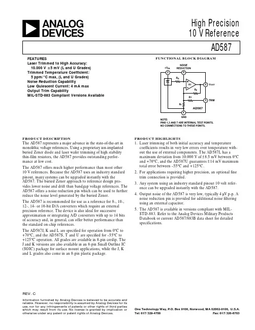
FUNCTIONAL BLOCK DIAGRAMREV.CInformation furnished by Analog Devices is believed to be accurate and reliable. However, no responsibility is assumed by Analog Devices for its use, nor for any infringements of patents or other rights of third parties which may result from its use. No license is granted by implication or otherwise under any patent or patent rights of Analog Devices.aHigh Precision 10 V ReferenceAD587One Technology Way, P.O. Box 9106, Norwood, MA 02062-9106, U.S.A.Tel: 617/329-4700Fax: 617/326-8703FEATURESLaser Trimmed to High Accuracy:10.000 V ؎5 mV (L and U Grades)Trimmed Temperature Coefficient:5 ppm/؇C max, (L and U Grades)Noise Reduction CapabilityLow Quiescent Current: 4 mA max Output Trim CapabilityMIL-STD-883 Compliant Versions AvailablePRODUCT HIGHLIGHTSser trimming of both initial accuracy and temperature coefficients results in very low errors over temperature with-out the use of external components. The AD587L has amaximum deviation from 10.000 V of ±8.5 mV between 0°C and +70°C, and the AD587U guarantees ±14 mV maximum total error between –55°C and +125°C.2.For applications requiring higher precision, an optional fine trim connection is provided.3.Any system using an industry standard pinout 10 volt refer-ence can be upgraded instantly with the AD587.4.Output noise of the AD587 is very low, typically 4 µV p-p. A noise reduction pin is provided for additional noise filtering using an external capacitor.5.The AD587 is available in versions compliant with MIL-STD-883. Refer to the Analog Devices Military Products Databook or current AD587/883B data sheet for detailed specifications.PRODUCT DESCRIPTION The AD587 represents a major advance in the state-of-the-art in monolithic voltage references. Using a proprietary ion-implanted buried Zener diode and laser wafer trimming of high stability thin-film resistors, the AD587 provides outstanding perfor-mance at low cost.The AD587 offers much higher performance than most other 10 V references. Because the AD587 uses an industry standard pinout, many systems can be upgraded instantly with the AD587. The buried Zener approach to reference design pro-vides lower noise and drift than bandgap voltage references. The AD587 offers a noise reduction pin which can be used to further reduce the noise level generated by the buried Zener.The AD587 is recommended for use as a reference for 8-, 10-,12-, 14- or 16-bit D/A converters which require an external precision reference. The device is also ideal for successiveapproximation or integrating A/D converters with up to 14 bits of accuracy and, in general, can offer better performance than the standard on-chip references.The AD587J, K and L are specified for operation from 0°C to +70°C, and the AD587S, T and U are specified for –55°C to +125°C operation. All grades are available in 8-pin cerdip. The J and K versions are also available in an 8-pin Small Outline IC (SOIC) package for surface mount applications, while the J, K and L grades also come in an 8-pin plastic package.NOISE V OUTTRIMGNDNOTE:PINS 1,3 AND 7 ARE INTERNAL TEST POINTS.NO CONNECTIONS TO THESE POINTS.AD587–SPECIFICATIONS(T A = +25؇C, V IN = +15 V unless otherwise noted)Model AD587J/S AD587K/T AD587L/UMin Typ Max Min Typ Max Min Typ Max Units OUTPUT VOLTAGE9.99010.0109.99510.0059.99510.005VOUTPUT VOLTAGE DRIFT10°C to +70°C20105ppm/°C –55°C to +125°C20105GAIN ADJUSTMENT+3+3+3%–1–1–1LINE REGULATION113.5 V ≤ + V IN≤ 36 VT MIN to T MAX100100100±µV/VLOAD REGULATION1Sourcing 0 < I OUT < 10 mAT MIN to T MAX100100100±µV/mA Sourcing –10 < I OUT < 0 mA2T MIN to T MAX100100100QUIESCENT CURRENT242424mAPOWER DISSIPATION303030mWOUTPUT NOISE0.1 Hz to 10 Hz444µV p-pSpectral Density, 100 Hz100100100nV/√HzLONG-TERM STABILITY151515±ppm/1000 Hr. SHORT-CIRCUIT CURRENT-TO-GROUND305030503050mASHORT-CIRCUIT CURRENT-TO-V IN305030503050mA TEMPERATURE RANGESpecified Performance (J, K, L)0+700+700+70°COperating Performance (J, K, L)3–40+85–40+85–40+85Specified Performance (S, T, U)–55+125–55+125–55+125Operating Performance (S, T, U)3–55+125–55+125–55+125NOTES1Spec is guaranteed for all packages and grades. Cerdip packaged parts are 100% production test.2Load Regulation (Sinking) specification for SOIC (R) package is ±200 µV/mA.3The operating temperature ranged is defined as the temperatures extremes at which the device will still function. Parts may deviate from their specified performance outside their specified temperature range.Specifications subject to change without notice.ORDERING GUIDEInitial Temperature Temperature PackageModel1Error Coefficient Range Options2AD587JQ10 mV20 ppm/°C0°C to +70°C Q-8AD587JR10 mV20 ppm/°C0°C to +70°C SO-8AD587JN10 mV20 ppm/°C0°C to +70°C N-8AD587KQ 5 mV10 ppm/°C0°C to +70°C Q-8AD587KR 5 mV10 ppm/°C0°C to +70°C SO-8AD587KN 5 mV10 ppm/°C0°C to +70°C N-8AD587LQ 5 mV 5 ppm/°C0°C to +70°C Q-8AD587LN 5 mV 5 ppm/°C0°C to +70°C N-8AD587SQ10 mV20 ppm/°C–55°C to +125°C Q-8AD587TQ10 mV10 ppm/°C–55°C to +125°C Q-8AD587UQ 5 mV 5 ppm/°C–55°C to +125°C Q-8AD587JCHIPS10 mV20 ppm/°C0°C to +70°CNOTES1For details on grade and package offerings screened in accordance with MIL-STD-883, refer to theAnalog Devices Military Products Databook or current AD587/883B data sheet.2N = Plastic DIP; Q = Cerdip; SO = SOIC.–2–REV. CAD587REV. C –3–ABSOLUTE MAXIMUM RATINGS*V IN to Ground . . . . . . . . . . . . . . . . . . . . . . . . . . . . . . . . . .36 V Power Dissipation (+25°C) . . . . . . . . . . . . . . . . . . . . .500 mW Storage Temperature . . . . . . . . . . . . . . . . . . .–65°C to +150°C Lead Temperature (Soldering, 10 sec) . . . . . . . . . . . . .+300°C Package Thermal ResistanceθJC . . . . . . . . . . . . . . . . . . . . . . . . . . . . . . . . . . . . . .22°C/W θJA . . . . . . . . . . . . . . . . . . . . . . . . . . . . . . . . . . . . .110°C/W Output Protection: Output safe for indefinite short to ground and momentary short to V IN .*Stresses above those listed under “Absolute Maximum Ratings” may cause permanent damage to the device. This is a stress rating only and functional operation of the device at these or any other conditions above those indicated in the operational sections of this specification is not implied. Exposure to absolute maximum rating conditions for extended periods may affect device reliability.DIE SPECIFICATIONSThe following specifications are tested at the die level for AD587JCHIPS. These die are probed at +25°C only.(T A = +25°C, V IN = +15 V unless otherwise noted)AD587JCHIPS Parameter Min Typ Max UnitsOutput Voltage 9.99010.010V Gain Adjustment –13%Line Regulation13.5 V < + V IN < 36 V 100±µV/V Load RegulationSourcing 0 < I OUT < 10 mA 100µV/mA Sinking –10 < I OUT < 0 mA 100µV/mA Quiescent Current24mA Short-Circuit Current-to-Ground 50mA Short-Circuit Currrent-to-V OUT50mANOTES 1Both V OUT pads should be connected to the output.2Sense and force grounds must be tied together.Die Thickness:The standard thickness of Analog Devices Bipolar dice is 24 mils ± 2 mils.Die Dimensions: The dimensions given have a tolerance of ±2 mils.Backing : The standard backside surface is silicon (not plated). Analog Devices does not recommend gold-backed dice for most applications.Edges: A diamond saw is used to separate wafers into dice thus providing perpendicular edges half-way through the die.In contrast to scribed dice, this technique provides a more uniform die shape and size . The perpen-dicular edges facilitate handling (such as tweezer pick-up) while the uniform shape and size simplifies substrate design and die attach.Top Surface: The standard top surface of the die is covered by a layer of glassivation . All areas are covered except bonding pads and scribe lines.Surface Metalization: The metalization to Analog Devices bipolar dice is aluminum. Minimum thickness is 10,000Å.Bonding Pads: All bonding pads have a minimum size of 4 mils by 4 mils. The passivation windows have 3.5 mils by 3.5 mils minimum.DIE LAYOUTPIN CONFIGURATIONTP *TRIMV OUTTP *NOISEREDUCTION+V IN TP *GND *TP DENOTES FACTORY TEST POINT. NO CONNECTIONS SHOULD BE MADE TO THESE PINS.Die Size: 0.081 × 0.060 InchesAD587REV. C–4–THEORY OF OPERATIONThe AD587 consists of a proprietary buried Zener diode refer-ence, an amplifier to buffer the output and several high stability thin-film resistors as shown in the block diagram in Figure 1.This design results in a high precision monolithic 10 V output reference with initial offset of 5 mV or less. The temperature compensation circuitry provides the device with a temperature coefficient of under 5 ppm/°C.NOISE V OUTTRIM GNDNOTE:PINS 1,3 AND 7 ARE INTERNAL TEST POINTS.NO CONNECTIONS TO THESE POINTS.Figure 1.AD587 Functional Block Diagram A capacitor can be added at the NOISE REDUCTION pin (Pin 8) to form a low-pass filter with R S to reduce the noise contribu-tion of the Zener to the circuit.APPLYING THE AD587The AD587 is simple to use in virtually all precision reference applications. When power is applied to Pin 2, and Pin 4 is grounded, Pin 6 provides a 10 V output. No external compo-nents are required; the degree of desired absolute accuracy is achieved simply by selecting the required device grade. The AD587 requires less than 4 mA quiescent current from an oper-ating supply of +15 V.Fine trimming may be desired to set the output level to exactly 10.000 V (calibrated to a main system reference). System cali-bration may also require a reference voltage that is slightly differ-ent from 10.000 V, for example, 10.24 V for binary applications.In either case, the optional trim circuit shown in Figure 2 can offset the output by as much as 300 mV, if desired, with mini-mal effect on other device characteristics.OUTPUTC Figure 2.Optional Fine Trim ConfigurationNOISE PERFORMANCE AND REDUCTIONThe noise generated by the AD587 is typically less than 4 µV p-p over the 0.1 Hz to 10 Hz band. Noise in a 1 MHz band-width is approximately 200 µV p-p. The dominant source of this noise is the buried Zener which contributes approximately 100 nV/√Hz . In comparison, the op amp’s contribution is negli-gible. Figure 3 shows the 0.1 Hz to 10 Hz noise of a typical AD587. The noise measurement is made with a bandpass filter made of a 1-pole high-pass filter with a corner frequency at 0.1 Hz and a 2-pole low-pass filter with a corner frequency at 12.6 Hz to create a filter with a 9.922 Hz bandwidth.Figure 3.0.1 Hz to 10 Hz NoiseIf further noise reduction is desired, an external capacitor may be added between the NOISE REDUCTION pin and ground as shown in Figure 2. This capacitor, combined with the 4 k Ω R S and the Zener resistances, form a low-pass filter on the output of the Zener cell. A 1 µF capacitor will have a 3 dB point at 40 Hz, and it will reduce the high frequency (to 1 MHz) noise to about 160 µV p-p. Figure 4 shows the 1 MHz noise of a typi-cal AD587 both with and without a 1 µF capacitor.Figure 4.Effect of 1 µF Noise Reduction Capacitor on Broadband Noise TURN-ON TIMEUpon application of power (cold start), the time required for the output voltage to reach its final value within a specified error band is defined as the turn-on settling time. Two components normally associated with this are: the time for the active circuits to settle, and the time for the thermal gradients on the chip to stabilize. Figure 5 shows the turn-on characteristics of theAD587. It shows the settling to be about 60 µs to 0.01%. Note the absence of any thermal tails when the horizontal scale is ex-panded to 1 ms/cm in Figure 5b.AD587REV. C–5–DYNAMIC PERFORMANCEThe output buffer amplifier is designed to provide the AD587 with static and dynamic load regulation superior to less com-plete references.Many A/D and D/A converters present transient current loads to the reference, and poor reference response can degrade the converter’s performance.Figure 6 displays the characteristics of the AD587 output ampli-fier driving a 0 mA to 10 mA load.Output turn-on time is modified when an external noise reduc-tion capacitor is used. When present, this capacitor acts as an additional load to the internal Zener diode’s current source, re-sulting in a somewhat longer turn-on time. In the case of a 1 µF capacitor, the initial turn-on time is approximately 400 ms to 0.01% (see Figure 5c).a.Electrical Turn-Onb.Extended Time Scalec.Turn-On with 1 µF C N Figure 5.Turn-On CharacteristicsFigure 6a.Transient Load Test Circuit Figure rge-Scale Transient Response Figure 6c.Fine Scale Settling for Transient LoadOUTAD587REV. C–6–In some applications, a varying load may be both resistive and capacitive in nature, or the load may be connected to the AD587 by a long capacitive cable.Figure 7 displays the output amplifier characteristics driving a 1000 pF, 0 mA to 10 mA load.V OUTFigure 7a.Capacitive Load Transient /Response Test CircuitFigure 7b.Output Response with Capacitive Load LOAD REGULATIONThe AD587 has excellent load regulation characteristics. Figure 8 shows that varying the load several mA changes the output by only a few µV.Figure 8.Typical Load Regulation Characteristics TEMPERATURE PERFORMANCEThe AD587 is designed for precision reference applications where temperature performance is critical. Extensive tempera-ture testing ensures that the device’s high level of performance is maintained over the operating temperature range.Some confusion exists in the area of defining and specifying ref-erence voltage error over temperature. Historically, references have been characterized using a maximum deviation per degree Centrigrade; i.e., ppm/°C. However, because of nonlinearities in temperature characteristics which originated in standard Zener references (such as “S” type characteristics), most manufactur-ers have begun to use a maximum limit error band approach to specify devices. This technique involves the measurement of the output at three or more different temperatures to specify an out-put voltage error band.Figure 9 shows the typical output voltage drift for the AD587L and illustrates the test methodology. The box in Figure 9 is bounded on the sides by thc operating temperature extremes,and on the top and the bottom by the maximum and minimum output voltages measured over the operating temperature range.The slope of the diagonal drawn from the lower left to the upper right corner of the box determines the performance grade of the device.Figure 9.Typical AD587L Temperature DriftEach AD587J, K, L grade unit is tested at 0°C, +25°C and +70°C. Each AD587S, T, and U grade unit is tested at –55°C,+25°C and +125°C. This approach ensures that the variations of output voltage that occur as the temperature changes within the specified range will be contained within a box whose diago-nal has a slope equal to the maximum specified drift. The posi-tion of the box on the vertical scale will change from device to device as initial error and the shape of the curve vary. The maxi-mum height of the box for the appropriate temperature range and device grade is shown in Figure 10. Duplication of these results requires a combination of high accuracy and stable temperature control in a test system. Evaluation of the AD587will produce a curve similar to that in Figure 9, but output readings may vary depending on the test methods and equip-ment utilized.Figure 10.Maximum Output Change in mVAD587REV. C –7–NEGATIVE REFERENCE VOLTAGE FROM AN AD587The AD587 can be used to provide a precision –10.000 V output as shown in Figure 11. The V IN pin is tied to at least a +3.5 V supply, the output pin is grounded, and the AD587 ground pin is connected through a resistor, R S , to a –15 V supply. The –10 V output is now taken from the ground pin (Pin 4) instead of V OUT . It is essential to arrange the output load and the sup-ply resistor R S so that the net current through the AD587 is be-tween 2.5 mA and 10.0 mA. The temperature characteristics and long-term stability of the device will be essentially the same as that of a unit used in the standard +10 V output configuration.1nF–15V–10VL <10mASFigure 11.AD587 as a Negative 10 V Reference USING THE AD587 WITH CONVERTERSThe AD587 is an ideal reference for a wide variety of 8-, 12-,14- and 16-bit A/D and D/A converters. Several representative examples follow.10 V REFERENCE WITH MULTIPLYING CMOS D/A OR A/D CONVERTERSThe AD587 is ideal for applications with 10- and 12-bit multi-plying CMOS D/A converters. In the standard hookup, as shown in Figure 12, the AD587 is paired with the AD754512-bit multiplying DAC and the AD711 high-speed BiFET Op Amp. The amplifier DAC configuration produces a unipolar 0 V to –10 V output range. Bipolar output applications and other operating details can be found on the individual product data sheets.Figure 12.Low Power 12-Bit CMOS DAC ApplicationThe AD587 can also be used as a precision reference for mul-tiple DACs. Figure 13 shows the AD587, the AD7628 dual DAC and the AD712 dual op amp hooked up for single supply operation to produce 0 V to –10 V outputs. Because both DACsare on the same die and share a common reference and output op amps; the DAC outputs will exhibit similar gain TCs.Figure 13. AD587 as a 10 V Reference for a CMOS Dual DACPRECISION CURRENT SOURCEThe design of the AD587 allows it to be easily configured as a current source. By choosing the control resistor R C in Figure 14,you can vary the load current from the quiescent current (2 mA typically) to approximately 10 mA.+V I L = + I BIAS10VR CFigure 14. Precision Current SourceAD587REV. C –8–P R I N T E D I N U . S . A . C 1 1 3 6 a –1 5–1 0 / 8 8PRECISION HIGH CURRENT SUPPLYFor higher currents, the AD587 can easily be connected to a power PNP or power Darlington PNP device. The circuit in Figure 15 can deliver up to 4 amps to the load. The 0.1 µF capacitor is required only if the load has a significant capacitive component. If the load is purely resistive, improved high fre-quency supply rejection results can be obtained by removing thecapacitor.Figure 15a. Precision High-Current Current Source Figure 15b.Precision High-Current Voltage SourceCerdip (Q-8) PackageMini-DIP (N-8) Package Small Outline (R-8) PackageOUTLINE DIMENSIONSDimensions shown in inches and (mm).。

V2406A SeriesCompact,fanless,vibration-proof railway computersFeatures and Benefits•Intel Celeron/Core i7processor•Dual independent DVI-I displays•2Gigabit Ethernet ports with M12X-coded connectors•1SATA connector and2CFast sockets for storage expansion•M12A-coded power connector•Compliant with EN50121-4•Complies with all EN50155mandatory test items1•Ready-to-run Debian7,Windows Embedded Standard7,and Windows10Embedded IoT Enterprise2016LTSB platforms•-40to70°C wide-temperature models available•Supports SNMP-based system configuration,control,and monitoring(Windows only)CertificationsIntroductionThe V2406A Series embedded computers are based on the Intel3rd Gen processor,and feature4RS-232/422/485serial ports,dual LAN ports, audio in/out,3USB2.0hosts,2CFast sockets,and1SATA storage socket.The V2406A computers provide dual DVI-I outputs,and in addition are compliant with the mandatory test items of the EN50155standard,making the computers suitable for a variety of industrial applications.The dual megabit/Gigabit Ethernet ports with M12X-coded connectors offer a reliable solution for network redundancy,promising continuous operation for data communication and management.As an added convenience,the V2406A computers have6DIs and2DOs for connecting digital input/output devices,and the CFast feature provides the reliability needed for industrial applications that require data buffering and storage expansion.Preinstalled with Linux Debian7or Windows Embedded Standard7,the V2406A Series provides programmers with a friendly environment for developing sophisticated,bug-free application software at a low cost.Wide-temperature models of the V2406A Series that operate reliably in a-40 to70°C operating temperature range are also available,offering an optimal solution for applications subjected to harsh environments.1.This product is suitable for rolling stock railway applications,as defined by the EN50155standard.For a more detailed statement,click here:/doc/specs/EN_50155_Compliance.pdfAppearanceFront ViewRear ViewSpecificationsComputerCPU V2406A-C2Series:Intel®Celeron®Processor1047UE(2M cache,1.40GHz)V2406A-C7Series:Intel®Core™i7-3517UE Processor(4M cache,up to2.80GHz) System Chipset Mobile Intel®HM65Express ChipsetGraphics Controller Intel®HD Graphics4000(integrated)System Memory Pre-installed4GB DDR3System Memory Slot SODIMM DDR3/DDR3L slot x1Supported OS Linux Debian7Windows Embedded Standard7(WS7E)32-bitWindows Embedded Standard7(WS7E)64-bitStorage Slot 2.5-inch HDD/SSD slots x1CFast slot x2Computer InterfaceEthernet Ports Auto-sensing10/100/1000Mbps ports(M12X-coded)x2Serial Ports RS-232/422/485ports x4,software selectable(DB9male)USB2.0USB2.0hosts x1,M12D-coded connectorUSB2.0hosts x2,type-A connectorsAudio Input/Output Line in x1,Line out x1,M12D-codedDigital Input DIs x6Digital Output DOs x2Video Output DVI-I x2,29-pin DVI-I connectors(female)Digital InputsIsolation3k VDCConnector Screw-fastened Euroblock terminalDry Contact On:short to GNDOff:openI/O Mode DISensor Type Dry contactWet Contact(NPN or PNP)Wet Contact(DI to COM)On:10to30VDCOff:0to3VDCDigital OutputsConnector Screw-fastened Euroblock terminalCurrent Rating200mA per channelI/O Type SinkVoltage24to30VDCLED IndicatorsSystem Power x1Storage x1LAN2per port(10/100/1000Mbps)Serial2per port(Tx,Rx)Serial InterfaceBaudrate50bps to921.6kbpsFlow Control RTS/CTS,XON/XOFF,ADDC®(automatic data direction control)for RS-485,RTSToggle(RS-232only)Isolation N/AParity None,Even,Odd,Space,MarkData Bits5,6,7,8Stop Bits1,1.5,2Serial SignalsRS-232TxD,RxD,RTS,CTS,DTR,DSR,DCD,GNDRS-422Tx+,Tx-,Rx+,Rx-,GNDRS-485-2w Data+,Data-,GNDRS-485-4w Tx+,Tx-,Rx+,Rx-,GNDPower ParametersInput Voltage12to48VDCPower Connector M12A-coded male connectorPower Consumption(Max.) 3.3A@12VDC0.82A@48VDCPower Consumption40W(max.)Physical CharacteristicsHousing AluminumIP Rating IP30Dimensions(with ears)275x63x154mm(10.83x2.47x6.06in) Dimensions(without ears)250x57x154mm(9.84x2.23x6.06in)Weight2,000g(4.44lb)Installation DIN-rail mounting(optional),Wall mounting(standard) Protection V2406A-C2-CT-T/C7-CT-T:PCB conformal coating Environmental LimitsOperating Temperature Standard Models:-25to55°C(-13to131°F)Wide Temp.Models:-40to70°C(-40to158°F) Storage Temperature(package included)-40to85°C(-40to185°F)Ambient Relative Humidity5to95%(non-condensing)Standards and CertificationsEMC EN55032/24EMI CISPR32,FCC Part15B Class AEMS IEC61000-4-2ESD:Contact:6kV;Air:8kVIEC61000-4-3RS:80MHz to1GHz:20V/mIEC61000-4-4EFT:Power:2kV;Signal:2kVIEC61000-4-5Surge:Power:2kVIEC61000-4-6CS:10VIEC61000-4-8PFMFRailway EN50121-4,IEC60571Railway Fire Protection EN45545-2Safety EN60950-1,UL60950-1Shock IEC60068-2-27,IEC61373,EN50155Vibration IEC60068-2-64,IEC61373,EN50155DeclarationGreen Product RoHS,CRoHS,WEEEMTBFTime332,173hrsStandards Telcordia(Bellcore),GBWarrantyWarranty Period3yearsDetails See /warranty Package ContentsDevice1x V2406A Series computer Installation Kit1x wall-mounting kit Documentation1x document and software CD1x quick installation guide1x warranty card DimensionsOrdering InformationModel Name CPU Memory(Default)OS CFast(CTO)Backup CFast(CTO)SSD/HDD Tray(CTO)Operating Temp.ConformalCoatingV2406A-C2Celeron1047UE4GB1(Optional)1(Optional)1(Optional)-25to55°C–V2406A-C2-T Celeron1047UE4GB1(Optional)1(Optional)1(Optional)-40to70°C–V2406A-C2-CT-T Celeron1047UE4GB1(Optional)1(Optional)1(Optional)-40to70°C✓V2406A-C7Core i7-3517UE4GB1(Optional)1(Optional)1(Optional)-25to55°C–V2406A-C7-T Core i7-3517UE4GB1(Optional)1(Optional)1(Optional)-40to70°C–V2406A-C7-CT-T i7-3517UE4GB1(Optional)1(Optional)1(Optional)-40to70°C✓V2406A-C2-W7E Celeron1047UE4GB8GB1(Optional)1(Optional)-25to55°C–V2406A-C2-T-W7E Celeron1047UE4GB8GB1(Optional)1(Optional)-40to70°C–V2406A-C7-T-W7E i7-3517UE4GB8GB1(Optional)1(Optional)-40to70°C–Accessories(sold separately)Battery KitsRTC Battery Kit Lithium battery with built-in connectorCablesCBL-M12(FF5P)/Open-100IP67A-coded M12-to-5-pin power cable,IP67-rated5-pin female M12connector,1mCBL-M12XMM8PRJ45-BK-100-IP67M12-to-RJ45Cat-5E UTP gigabit Ethernet cable,8-pin X-coded male connector,IP67,1m ConnectorsM12A-5PMM-IP685-pin male circular threaded D-coded M12USB connector,IP68M12X-8PMM-IP678-pin male X-coded circular threaded gigabit Ethernet connector,IP67M12A-5P-IP68A-coded screw-in sensor connector,female,IP68,4.05cmM12A-8PMM-IP678-pin male circular threaded A-codes M12connector,IP67-rated(for field-installation)Power AdaptersPWR-24270-DT-S1Power adapter,input voltage90to264VAC,output voltage24V with2.5A DC loadPower CordsPWC-C7AU-2B-183Power cord with Australian(AU)plug,2.5A/250V,1.83mPWC-C7CN-2B-183Power cord with two-prong China(CN)plug,1.83mPWC-C7EU-2B-183Power cord with Continental Europe(EU)plug,2.5A/250V,1.83mPWC-C7UK-2B-183Power cord with United Kingdom(UK)plug,2.5A/250V,1.83mPWC-C7US-2B-183Power cord with United States(US)plug,10A/125V,1.83mAntennasANT-WDB-ANF-0407 2.4/5GHz,omni-directional antenna,4/7dBi,N-type(male)Wall-Mounting KitsV2400Isolated Wall Mount Kit Wall-mounting kit with isolation protection,2wall-mounting brackets,4screwsStorage KitsFK-75125-02Storage bracket,4large silver screws,4soft washers,4small sliver bronze screws,1SATA powercable,4golden spacers(only for the V2406and V2426)DIN-Rail Mounting KitsDK-DC50131DIN-rail mounting kit,6screws©Moxa Inc.All rights reserved.Updated Jun12,2019.This document and any portion thereof may not be reproduced or used in any manner whatsoever without the express written permission of Moxa Inc.Product specifications subject to change without notice.Visit our website for the most up-to-date product information.。
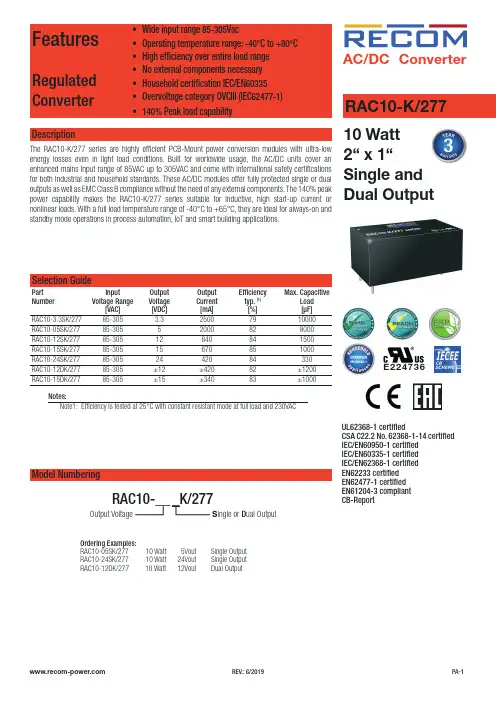
AC/DC ConverterE22473610 Watt 2“ x 1“Single andDual OutputFeaturesRegulated Converter• Wide input range 85-305Vac• Operating temperature range: -40°C to +80°C • High effi ciency over entire load range • No external components necessary • Household certifi cation IEC/EN60335• Overvoltage category OVCIII (IEC62477-1)• 140% Peak load capabilityDescriptionThe RAC10-K/277 series are highly effi cient PCB-Mount power conversion modules with ultra-low energy losses even in light load conditions. Built for worldwide usage, the AC/DC units cover an enhanced mains input range of 85VAC up to 305VAC and come with international safety certifi cations for both industrial and household standards. These AC/DC modules offer fully protected single or dual outputs as well as EMC Class B compliance without the need of any external components. The 140% peak power capability makes the RAC10-K/277 series suitable for inductive, high start-up current or nonlinear loads. With a full load temperature range of -40°C to +65°C, they are ideal for always-on and standby mode operations in process automation, IoT and smart building applications.RAC10-K/277UL62368-1 certifi edCSA C22.2 No. 62368-1-14 certifi ed IEC/EN60950-1 certifi ed IEC/EN60335-1 certifi ed IEC/EN62368-1 certifi ed EN62233 certifi ed EN62477-1 certifi ed EN61204-3 compliantCB-ReportSelection GuidePart Input Output Output Effi ciency Max. Capacitive Number Voltage Range Voltage Current typ. (1) Load [VAC] [VDC] [mA] [%] [µF]RAC10-3.3SK/277 85-305 3.3 2500 79 10000RAC10-05SK/277 85-305 5 2000 82 8000RAC10-12SK/277 85-305 12 840 84 1500RAC10-15SK/277 85-305 15 670 85 1000RAC10-24SK/277 85-305 24 420 84 330RAC10-12DK/277 85-305 ±12 ±420 82 ±1200RAC10-15DK/277 85-305 ±15 ±340 83 ±1000Notes:Note1: Effi ciency is tested at 25°C with constant resistant mode at full load and 230VACModel NumberingS ingle or D ual OutputOutput VoltageRAC10-__ _K/277Ordering Examples:RAC10-05SK/277 10 Watt 5Vout Single Output RAC10-24SK/277 10 Watt 24Vout Single Output RAC10-12DK/277 10 Watt 12Vout Dual OutputSpecifi cations (measured @ Ta= 25°C, nominal input voltage (115/230VAC), full load and after warm-up)Specifi cations (measured @ Ta= 25°C, nominal input voltage (115/230VAC), full load and after warm-up)REGULATIONSParameter Condition Value Output Accuracy±1.0% typ. Line Regulation low line to high line±0.5% typ.Load Regulation0-100% load 3.3, 5Voutothers1.5% typ.1.0% typ.Cross Regulation dual output only±10.0% typ.Transient Response 25% load step changerecovery time4.0% max.500µsSpecifi cations (measured @ Ta= 25°C, nominal input voltage (115/230VAC), full load and after warm-up)PROTECTIONSParameter Type Value Input Fuse (4)T2A, slow blow Short Circuit Protection (SCP)Hiccup, automatic restart Over Voltage Protection (OVP)150% - 195%, latch off mode Over Load Protection (OLP)150% - 195%, hiccup mode Over Voltage Category (OVC)according to IEC/EN61477-1OVC III Class of Equipment Class II Isolation Voltage tested for 1 minute4kVACIsolation ResistanceI/P to O/P Isolation Voltage 500VDC1GΩ min.Isolation Capacitance100kHz/0.1V100pF max. Insulation Grade reinforced Leakage Current0.25mA max.Notes:Specifi cations (measured @ Ta= 25°C, nominal input voltage (115/230VAC), full load and after warm-up)SAFETY AND CERTIFICATIONSCertifi cate Type (Safety)Report / File Number StandardAudio/Video, information and communication technology equipment - Safety requirements E224736UL62368-1, 2nd Edition, 2014CAN/CSA C22.2 No. 62368-1-14, 2nd Edition, 2014Information Technology Equipment, General Requirements for Safety (CB Scheme)E491408-A4-CB-1IEC60950-1:2005, 2nd Edition + A2:2013Information Technology Equipment, General Requirements for Safety (LVD)EN60950-1:2006 + A2:2013Household and similar electrical appliances - Safety - Part 1: General requirements LCS170821028CSIEC60335-1:2010 + A2:2016 + C1:2016, 5th EditionEN60335-1:2012 + A11:2014Audio/Video, information and communication technology equipment - Safetyrequirements (CB Scheme)16BCS10045 11IEC62368-1:2014, 2nd EditionAudio/Video, information and communication technology equipment - Safetyrequirements (LVD)EN62368-1:2014 + A11:2017 Measurement methods for electromagnetic fi elds of household appliancesand similar apparatus with regard to human exposureLCS170821028CS EN62233:2008Safety requirements for power electronic converter systems and equipment - Part 1: General LCS181212006CSIEC62477-1:2012 + A1:2016, 1st EditionEN62477-1: 2012 + A1:2017Specifi cations (measured @ Ta= 25°C, nominal input voltage (115/230VAC), full load and after warm-up)DIMENSION and PHYSICAL CHARACTERISTICSParameterTypeValueMaterial case potting PCB baseplateblack plastic (UL94V-0)silicone (UL94V-0)FR4 (UL94V-0)plastic (UL94V-0)Dimension (LxWxH)52.5 x 27.4 x 23.0mmWeight65g typ.Certifi cate Type (Safety)Report / File NumberStandard EAC Safety of Low Voltage Equipment RU-AT.03.67361TP TC 004/020, 2011RoHS2+RoHS 2011/65/EU + AM2015/863EMC ComplianceConditionsStandard / CriterionLow-voltage power supplies DC output - Part 3: Electromagnetic compatibility LCS170821088AE EN61204-3:2000, Class BInformation technology equipment - Radio disturbance characteristics - Limits and methods of measurement AS/NZS CSPR 22:2009 + A1:2010, Class BESD Electrostatic discharge immunity test±8kV Air; ±4kV Contact EN61000-4-2: 2009, Criteria BRadiated, radio-frequency, electromagnetic fi eld immunity test 10V/m, 80MHz-1GHz 3V/m, 1.5GHz-2GHz 1V/m, 2GHz-2.7GHz EN61000-4-3: 2006 + A2, 2010, Criteria AFast Transient and Burst Immunity AC In Port: ±2.0kV DC Out Port: ±2.0kV EN61000-4-4:2012, Criteria B Surge ImmunityAC In Port: ±1.0kV L-PE, N-PE ±2.0kV DC Out Port: ±0.5kVEN61000-4-5:2014, Criteri B Immunity to conducted disturbances, induced by radio-frequency fi elds 10VrmsEN61000-4-6:2014, Criteria A Power Magnetic Field Immunity 50Hz, 1A/m EN61000-4-8:2010, Criteria A Voltage Dips and InterruptionsVoltages Dips: >95%Voltage Dips: 30%Interruptions: >95%EN61000-4-11: 2004, Criteria B EN61000-4-11: 2004, Criteria C EN61000-4-11: 2004, Criteria CVoltage Fluctuations and Flicker in Public Low-Voltage Systems <=16A per phaseEN61000-3-3: 2013Notes:Note6: If output is connected to GND, please contact RECOM tech support for adviceSpecifi cations (measured @ Ta= 25°C, nominal input voltage (115/230VAC), full load and after warm-up) ArrayPACKAGING INFORMATIONParameter Type Value Packaging Dimension (LxWxH)tube490.0 x 56.0 x 40.0mm Packaging Quantity15pcs Storage Temperature Range-40°C to +85°C Storage Humidtiy non-condensing20% to 90% RHThe product information and specifications may be subject to changes even without prior written notice.The product has been designed for various applications; its suitability lies in the responsibility of each customer. Theproducts are not authorized for use in safety-critical applications without RECOM’s explicit written consent. A safety-critical application is an application where a failure may reasonably be expected to endanger or cause。
intel cpu型号大全2009年12月24日星期四 15:12intel cpu型号大全按照处理器支持的平台来分,Intel处理器可分为台式机处理器、笔记本电脑处理器以及工作站/服务器处理器三大类;下面我们将根据这一分类为大家详细介绍不同处理器名称的含义与规格。
由于Intel产品线跨度很长,不少过往产品已经完全或基本被市场淘汰(比如奔腾III和赛扬II),为了方便起见,我们的介绍也主要围绕P4推出后Intel发布的处理器产品展开。
台式机处理器Pentium 4(P4)第一款P4处理器是Intel在2000年11月21日发布的P4 1.5GHz处理器,从那以后到现在近四年的时间里,P4处理器随着规格的不断变化已经发展成了具有近10种不同规格的处理器家族。
在这里面,“P4 XXGHz”是最简单的P4处理器型号。
这其中,早期的P4处理器采用了Willamette核心和Socket 423封装,具256KB二级缓存以及400MHz前端总线。
之后由于接口类型的改变,又出现了采用illamette核心和Socket478封装的 P4产品。
而目前我们所说的“P4”一般是指采用了Northwood核心、具有400MHz前端总线以及512KB二级缓存、基于Socket 478封装的P4处理器。
虽然规格上不一样,不过这些处理器的名称都采用了“P4 XXGHz”的命名方式,比如P4 1.5GHz、P4 1.8GHz、P4 2.4GHz。
Pentium 4 A(P4 A)有了P4作为型号基准,那么P4 A就不难理解了。
在基于Willamette核心的P4处理器推出后不久,Intel为了提升处理器性能,发布了采用Northwood 核心、具有 400MHz前端总线以及512KB二级缓存的新一代P4。
由于这两种处理器在部分频率上发生了重叠,为了便于消费者辨识,Intel就在出现重叠的、基于Northwood核心的P4处理器后面增加一个大写字母“A”以示区别,于是就诞生了P4 1.8A GHz、P4 2.0A GHz这样的处理器产品。


施耐德自动化产品技术问答2006-11-11 02:57223,问:我用的PLC是PC-E984-258, 但当配置了AS-BDEP217并下载后启动PLC 时, 出现错误, 错误代码为4000, PLC 无法运行, 如何解决?当使用PC-A984-1xx, PC-E984-24x与PC-E984-25x系列的PLC时, 对某些A120I/O模块需要下载loadables, 具体说明如下:1. 要支持DEP211,DEP214,DEP215,DEP217与DAP217,需下载Dsc1.dat文件2. 要支持ADU214, 需下载Adu214.dat文件3. 要支持ADU216, 需下载Adu216.dat文件出现上面现象的原因就是没有下载支持DEP217的Dsc1.dat文件, 只要下载该文件, 以上故障即可排除..224,问:如何将ProWorx软件授权从一台PC机移到另一台PC机里?1. 将 ProWorx 软件安装到目标PC机中2. 点击”help”→”product authorization”→”software keys”, 然后记下界面右上角的”sitecode number”3. 返回源PC机, 点击”help”→”product authorization”→”software keys”→”move”→”next”4. 输入目标PC机中的”site code number”, 点击”next”, 并确认5. 插入空白软盘, 点击”next”→”finish”→”ok”6. 返回目的PC机, 点击”add”→”authorize by disk”→”next”7. 插入授权软盘, 点击”next”→”finish”→”ok”, 授权移机完成225,问:Premium,Micro通过TSXFPP10作为FIPIO agent时,如何与FIPIO主站进行数据交换?FIPIO agent与FIPIO主站之间通过共享变量的方式,进行数据交换。
NTE27C64−15DIntegrated Circuit64 Kbit (8Kb x 8) UV EPROMDescription:The NTE27C64−15D is a 64Kbit UV EPROM in a 28−Lead DIP type package ideally suited for micro-processor systems requiring large programs and is organized as 8,192 by 8 bits. This device has a transparent lid which allows the user to expose the chip to ultraviolet light to erase the bit pattern. A new pattern can then be written to the device by following the programming procedure.Features:D5V ±10% Supply Voltage in Read OperationD Access Time: 100nsD Low Power “CMOS” Consumption:−Active Current 30mA−Standby Current 100µAD Programming Voltage: 12.5V ±0.25VAbsolute Maximum Ratings: (Note 1). . . . . . . . . . . . . . . . . . . . . . . . . . . . . . . . . . . . . . . . . . . . . . . . . . . . . . . . . . .Supply Voltage, V CC−2 to +7V. . . . . . . . . . . . . . . . . . . . . . . . . . . . . . . . . .Input or Output Voltage (Except A9, Note 2), V IO−2 to +7V A9 Voltage (Note 2), V A9−2 to +13.5V. . . . . . . . . . . . . . . . . . . . . . . . . . . . . . . . . . . . . . . . . . . . . . . . . . . .. . . . . . . . . . . . . . . . . . . . . . . . . . . . . . . . . . . . . . . . . . . . . . . . . .Program Supply Voltage, V PP−2 to +14V. . . . . . . . . . . . . . . . . . . . . . . . . . . . . . . . . .Ambient Operating Temperature Range, T A−40° to +125°C Temperature Under Bias Range, T BIAS−50° to +125°C. . . . . . . . . . . . . . . . . . . . . . . . . . . . . . . . . . . . . .. . . . . . . . . . . . . . . . . . . . . . . . . . . . . . . . . . . . . . . . .Storage Temperature Range, T STG−65° to +150°C Note 1.Except for the rating “Operating Temperature Range”, stresses above those listed in the table “Absolute Maximum Ratings” may cause permanent damage to the device. These are stress ratings only and operation of the device at these or any other conditions above those indicated in the Operating sections of this specification is not implied. Exposure to Absolute Maximum Rating conditions for extended periods may affect device reliability.Note 2.Minimum DC voltage on the input or output is −0.5V with possible undershoot to −2.0V fora period less than 20ns. Maximum DC voltage on output is V CC +0.5V with possible over-shoot to V CC +2V for a period less than 20ns.Device Operation:The modes of operation of the NTE27C64 are listed in the Operating Modes table. A single power supply is required in the read mode. All inputs are TTL levels except for V PP and 12V on A9. Read Mode:The NTE27C64 has two control functions, both of which must be logically active in order to obtain data at the outputs. Chip Enable (E) is the power control and should be used for device selection. Output Enable (G) is the output control and should be used to gate data to the output pins, independent of device selection. Assuming that the addresses are stable, the address access time (t AVQV) is equal to the delay from E to output (t ELQV). Data is available at the output after a delay of t GLQV from the falling edge of G, assuming that E has been low and the addresses have been stable for at least t AVQV−t GLQV.Operating Modes:Note: X = V IH or V IL, V ID = 12V ±0.5V.Capacitance: (T = +25°C, f = 1MHz, Note 3 unless otherwise specified)Note 3.Sampled only, not 100% tested.Standby Mode:The NTE27C64has a standby mode which reduces the active current from 30mA to 100µA. The NTE27C64 is placed in the standby mode by applying a CMOS high signal to the E input. When in the standby mode, the outputs are in a high impedance state, independent of the G input.Two Line Output Control:Because EPROMs are usually used in larger memory arrays, this product features a 2 line control function which accommodates the use of multiple memory connection. The two line control function allows:a.The lowest possible memory power dissipation,plete assurance that output bus connection will not occur.For the most efficient use of these two control lines, E should be decoded and used as the primary device selecting function, while G should be made a common connection to all devices in the array and connected to the READ line from the system control bus. This ensures that all deselected memory devices are in their low power standby mode and that the output pins are only active when data is required from a particular memory device.Read Mode DC Characteristics:(T A = 0° to +70°C, V CC = 5V ±10%, V PP = V CC, Note 4 unlessotherwise specified)Note 4.V CC must be applied simultaneously with or before V PP and removed simultaneously or after V PP. Note 5.Maximum DC voltage on output is V CC +0.5V.System Considerations:The power switching characteristics of Advanced CMOS EPROMs require careful decoupling of the devices. The supply current, I CC, has three segments that are of interest to the system designer: the standby current level, the active current level, and transient current peaks that are produced by the falling and rising edges of E. The magnitude of the transient current peaks is dependent on the capaci-tive and inductive loading of the device at the output. The associated transient voltage peaks can be suppressed by complying with the two line output control and by properly selected decoupling capaci-tors. It is recommended that a 0.1µF ceramic capacitor be used on every device between V CC and V SS. This should be a high frequency capacitor of low inherent inductance and should be placed as close to the device as possible. In addition, a 4.7µF bulk electrolytic capacitor should be used between V CC and V SS for every eight devices. The bulk capacitor should be located near the power supply connection point. The purpose of the bulk capacitor is to overcome the voltage drop caused by the inductive effects of PCB traces.Read Mode AC Characteristics:(T A = 0° to +70°C, V CC = 5V ±10%, V PP = V CC, Note 4 unlessotherwise specified)Note 3.Sampled only, not 100% tested.Note 4.V CC must be applied simultaneously with or before V PP and removed simultaneously or after V PP.Programming Mode DC Characteristics:(T A = +25°C, V CC = 6V ±0.25V, V PP = 12.5V ±0.25V,Note 4 unless otherwise specified)Note 4.V CC must be applied simultaneously with or before V PP and removed simultaneously or after V PP.Programming Mode AC Characteristics:(T A = +25°C, V CC = 6V ±0.25V, V PP = 12.5V ±0.25V,Note 4 unless otherwise specified)Note 3.Sampled only, not 100% tested.Note 4.V CC must be applied simultaneously with or before V PP and removed simultaneously or after V PP.Programming:When delivered (and after each erasure for UV EPROM), all bits of the NTE27C64 are in the “1” state. Data is introduced by selectively programming “0”s into the desired bit locations. Although only “0”s will be programmed, both “1”s and “0”s can be present in the data word. The only way to change a “0” to a “1” is by die exposure to ultraviolet light (UV EPROM). The NTE27C64 is in the programming mode when V PP input is at 12,5V, E is at V IL and P is pulsed to V IL. The data to be programmed is applied to 8 bits in parallel to the data output pins. The levels required for the address and data inputs are TTL. V CC is specified to be 6V ±0.25V.Program Inhibit:Programming of multiple NTE27C64s in parallel with different data is also easily accomplished. Ex-cept for E, all like inputs including G of the parallel NTE27C64 may be common. A TTL low level pulse applied to an NTE27C64’s P input, with E low and V PP at 12.5V, will program that NTE27C64. A high level E input inhibits the other NTE27C64s from being programmed.Program Verify:A verify (read) should be performed on the programmed bits to determine that they were correctly programmed. The verify is accomplished with E and G at V IL, P at V IH, V PP at 12.5V and V CC at 6V. Erasure Operation:The erasure characteristics of the NTE27C64 is such that erasure begins when the cells are exposed to light with wavelengths shorter than approximately 4000Å. It should be noted that sunlight and some type of fluorescent lamps have wavelengths in the 3000−4000Å range. Research shows that constant exposure to room level fluorescent lighting could erase a typical NTE27C64 in about 3 years, while it would take approximately 1 week to cause erasure when exposed to direct sunlight. If the NTE27C64 is to be exposed to these types of lighting conditions for extended periods of time, it is suggested that opaque labels be put over the NTE27C64 window to prevent unintentional erasure. The recommended erasure procedure for the NTE27C64 is exposure to short wave ultraviolet light which has a wavelength of 2537Å. The integrated dose (i.e. UV intensity x exposure time) for erasure should be a minimum of 15W−sec/cm2. The erasure time with this dosage is approximately 15 to 20 minutes using an ultraviolet lamp with 12000µW/cm2 power rating. The NTE27C64 should be placed within 2.5cm (1 inch) of the lamp tubes during the erasure. Some lamps have a filter on their tubes which should be removed before erasure.。
The V464 embedded computers are based on the AMD x86 processor, and feature 4 serial ports, quad LAN ports, 4 USB 2.0 hosts, and CompactFlash. A VGA interface is also included, making the V464 computers particularly well-suited for industrial applications such as SCADA and factory automation.The V464 computers’ 4 serial ports can be used to connect a wide range of serial devices, and the quad 10/100 Mbps Ethernet ports offer a reliable solution for network redundancy, promising continuousFront Viewoperation for data communication and management. In addition, the CompactFlash and USB sockets provide the V464 computers with the reliability needed for industrial applications that require data buffering and storage expansion.The V464 computers come with the WinCE 6.0 or WinXP Embedded operating system already installed. WinCE 6.0 and WinXP Embedded provide programmers with a friendly environment for developingsophisticated, bug-free application software at a lower cost.OverviewAppearanceRear View10/100 Mbps SocketSerial Ports x 2Serial Ports x 2 9-36 VDCComputerCPU:******************************************,500 MHzOS (pre-installed): Windows CE 6.0 or Windows XP Embedded System Chipset: AMD CS5536BIOS: 4 Mbit Flash BIOS, supporting Plug & Play, APM 1.2, ACPI 1.0 SRAM: 256 KB, battery backupFSB: 400 MHzSystem Memory: 200-pin SO-DIMM socket with built-in 256 MB (CE) or 512 MB (XPe) DDR, supporting DDR400 up to 1 GB Expansion Bus: PC/104-Plus onboardUSB: USB 2.0 compliant hosts x 4, type A connector, supports system boot upStorageBuilt-in: 256 MB (CE) or 1 GB (XPe) industrial DOM for OS Storage Expansion: CompactFlash socketOther PeripheralsKB/MS: 1 PS/2 interface supporting standard PS/2 keyboard and mouse through Y-type cableAudio: AC97 audio, with line-out interfaceDisplayGraphics Controller: CPU integrated 2D graphicsDisplay Interface: CRT interface for VGA outputEthernet InterfaceLAN: 4 10/100 Mbps, auto-sensing (RJ45) portsController: Realtek RTL8100CLMagnetic Isolation Protection: 1.5 KV built-inSerial InterfaceSerial Standards:• 2 RS-232 ports (DB9 male)• 2 RS-232/422/485 ports, software selectable (DB9 male)ESD Protection: 15 KV for all signalsSerial Communication ParametersData Bits: 5, 6, 7, 8Stop Bits: 1, 1.5, 2Parity: None, Even, Odd, Space, MarkFlow Control: RTS/CTS, XON/XOFF, ADDC® (automatic data direction control) for RS-485Baudrate: 50 bps to 921.6 Kbps (non-standard baudrates supported; see user’s manual for details)Serial SignalsRS-232: TxD, RxD, DTR, DSR, RTS, CTS, DCD, GNDRS-422: TxD+, TxD-, RxD+, RxD-, GND RS-485-4w: TxD+, TxD-, RxD+, RxD-, GNDRS-485-2w: Data+, Data-, GNDLEDsSystem: Power, Battery, StorageLAN: 10M/Link x 2, 100M/Link x 2 (on connector)Switches and ButtonsPower Switch: on/offReset Button: For warm rebootPhysical CharacteristicsHousing: AluminumWeight: 1.32 kgDimensions:Without ears: 223 x 121 x 57 mm (8.78 x 4.76 x 2.24 in)With ears: 248 x 140 x 70 mm (9.76 x 5.51 x 2.76 in)Mounting: DIN-Rail, wallEnvironmental LimitsOperating Temperature: -10 to 60°C (14 to 140°F)Operating Humidity: 5 to 95% RHStorage Temperature: -20 to 80°C (-4 to 176°F)Anti-vibration: 5 g rms @ IEC-68-2-34, random wave, 5-500 Hz, 1 hr per axisAnti-shock: 50 g @ IEC-68-2-27, half sine wave, 11 msPower RequirementsInput Voltage: 9 to 36 VDC (3-pin terminal block for V+, V-, SG) Power Consumption: 26 W• 730 mA @ 36 VDC• 1080 mA @ 24 VDC• 2820 mA @ 9 VDCRegulatory ApprovalsEMC: CE (EN55022 Class A, EN61000-3-2 Class A, EN61000-3-3, EN55024), FCC (Part 15 Subpart B, CISPR 22 Class A), CCC (GB9254, GB 17625.1)Safety: UL/cUL (UL60950-1, CSA C22.2 No. 60950-1-03), LVD, CCC (GB4943)Green Product: RoHS, cRoHS, WEEEReliabilityAlert Tools: Built-in buzzer and RTC (real-time clock) with battery backupAutomatic Reboot Trigger: Built-in WDT (watchdog timer) supporting 1-255 level time interval system reset, software programmable WarrantyWarranty Period: 3 yearsDetails: See /warrantyHardware SpecificationsWindows Embedded CE 6.0System Utilities: Windows command shell, telnet, ftpFile System: FAT (on-board flash)Protocol Stack: TCP, UDP, IPv4, SNMP V2, ICMP, IGMP, ARP, HTTP, CHAP, PAP, SSL, DHCP, SNTP, SMTP, Telnet, FTP, PPP Telnet Server: Allows remote administration through a standard telnet client.FTP Server: Used for transferring files to and from remote computer systems over a network.File Server: Enables clients to access files and other resources over the network (Microsoft® Wincows® CE).Web Server (httpd): Includes ASP, ISAPI Secure Socket Layer support, SSL 2, SSL 3, and Transport Layer Security (TLS/SSL 3.1) public key-based protocols, and Web Administration ISAPI Extensions.Dial-up Networking Service: RAS client API and PPP, supporting Extensible Authentication Protocol (EAP) and RAS scripting. Watchdog Service: CPU Hardware function to reset CPU in a user specified time interval (triggered by calling a MOXA library function).Application Development Software:• Moxa WinCE 6.0 SDK• C Libraries and Run-times• Component Services (COM and DCOM)• Microsoft® .NET Compact Framework 2.0 SP2• XML, including DOM, XQL, XPATH, XSLT, SAX, SAX2• SOAP Toolkit Client• Winsock 2.2Software SpecificationsWindows XP EmbeddedSystem Utilities: Windows command shell, Telnet, ftp, Wireless Zero Configuration File System: NTFSProtocol Stack: DHCP, IPv4, DNS, IPsec, HTTP, TCP, UDP, ICMP, IGMP, ARP, TAPI, TSP, SNMP V2, NTP, ICS, PPP, CHAP, EAP, SNTP, Telnet, SNTP, FTP, SMTP, PPPoE, PPTP, NetBIOSTelnet Server: Allows users to connect to Telnet servers from remote computers.IIS Web Server: Allows you to create and manage Web sites.Terminal Server: Microsoft Terminal Server client application (mstsc.exe).COM+ Services: The next evolution of Microsoft Component Object Model (COM) and Microsoft Transaction Server (MTS).Computer Browser Service: Computer browsing functionalityexposed by Windows through Microsoft Networking. Allows a client machine to browse its network neighborhood for available computers exposing file and print sharing services.Disk Management Services: Support for disk and volumemanagement operations. The component implements a Component Object Model (COM) interface that can be used to query and configure disks and volumes, both basic and dynamic. The component also monitors disk arrivals and removals and other changes in the storage subsystem.Remote Registry Service: Enables remote users to modify registry settings on this computer.Application Development Software:• Microsoft .Net Framework 2.0 with service pack 2 (CLR and the .NET Framework class library)• Active Directory Service Interface (ADSI) Core • Active Template Library (ATL), 2.0• Certificate Request Client & Certificate Autoenrollment (CLR and the .NET Framework class library) • COM APIs• Common Control Libraries • Common File Dialogs• Direct3D, DirectPlay, DirectShow and Direct show filters • Distributed Transaction Coordinator (MSDTC)• Enhanced Write Filter (Redirect disk write operations to volatile (RAM) or non-volatile (disk) storage) • Event Log, Internet Explorer • Mapi32 Libraries• Message Queuing (MSMQ) Core• Microsoft Visual C++ Run Time Libraries • Power Management dynamic-link library • Registry Editor • RPC• Smart Card Cryptographic Service Providers• USB 2.0 core drivers compliant with The USB .95 or 1.0 • Windows API, Media Player 10, Script Engines, and WMIV464 computer• Ethernet cable: RJ45 to RJ45 cross-over • cable, 100 cmDIN-rail Mounting Kit• PS2 to KB/MS Y-type Cable• Document and Software CD or DVD • Quick Installation Guide (printed)• Product Warranty Statement (printed)• Package ChecklistAvailable ModelsV464-CE: x86 embedded computer with 4 serial ports, quad LANs, VGA, CompactFlash, USB, and WinCE 6.0 OSV464-XPE: x86 embedded computer with 4 serial ports, quad LANs, VGA, CompactFlash, USB, and Windows XP Embedded OSOptional Accessories (can be purchased separately)PWR-24250-DT-S1: Power adaptorPWC-C7US-2B-183: Power cord with 2-pin connector, USA plug PWC-C7EU-2B-183: Power cord with 2-pin connector, Euro plug PWC-C7UK-2B-183: Power cord with 2-pin connector, British plug PWC-C7AU-2B-183: Power cord with 2-pin connector, Australia plug PWC-C7CN-2B-183: Power cord with 2-pin connector, China plugOrdering Information。
TMS320C66x DSPCPU and Instruction Set Reference GuideLiterature Number:SPRUGH7November 2010 Release HistoryRelease Date Chapter/Topic Description/CommentsNovember 2010All Initial release based on TMS320C674x CPU and Instruction Set Reference Guide(SPRUFE8)ø-ii TMS320C66x DSP CPU and Instruction Set Reference Guide SPRUGH7—November 2010Submit Documentation FeedbackContents SPRUGH7—November 2010TMS320C66x DSP CPU and Instruction Set Reference Guide ø-iii Submit Documentation Feedback ContentsRelease History. . . . . . . . . . . . . . . . . . . . . . . . . . . . . . . . . . . . . . . . . . . . . . . . . . . . . . . . . . . . . . . . . . . . . . . . . . . . . . . . . . . . . . . . . . . . . . . . . . . . . . . ø-iiList of Tables. . . . . . . . . . . . . . . . . . . . . . . . . . . . . . . . . . . . . . . . . . . . . . . . . . . . . . . . . . . . . . . . . . . . . . . . . . . . . . . . . . . . . . . . . . . . . . . . . . . . . . . ø-xviiList of Figures . . . . . . . . . . . . . . . . . . . . . . . . . . . . . . . . . . . . . . . . . . . . . . . . . . . . . . . . . . . . . . . . . . . . . . . . . . . . . . . . . . . . . . . . . . . . . . . . . . . . . . . ø-xx List of Examples. . . . . . . . . . . . . . . . . . . . . . . . . . . . . . . . . . . . . . . . . . . . . . . . . . . . . . . . . . . . . . . . . . . . . . . . . . . . . . . . . . . . . . . . . . . . . . . . . . . .ø-xxivPreface ø-xxvAbout This Manual. . . . . . . . . . . . . . . . . . . . . . . . . . . . . . . . . . . . . . . . . . . . . . . . . . . . . . . . . . . . . . . . . . . . . . . . . . . . . . .ø-xxvNotational Conventions. . . . . . . . . . . . . . . . . . . . . . . . . . . . . . . . . . . . . . . . . . . . . . . . . . . . . . . . . . . . . . . . . . . . . . . . . .ø-xxvRelated Documentation from Texas Instruments. . . . . . . . . . . . . . . . . . . . . . . . . . . . . . . . . . . . . . . . . . . . . . . . . ø-xxviTrademarks. . . . . . . . . . . . . . . . . . . . . . . . . . . . . . . . . . . . . . . . . . . . . . . . . . . . . . . . . . . . . . . . . . . . . . . . . . . . . . . . . . . . . ø-xxvi Chapter 1Introduction1-11.1DSP Features and Options. . . . . . . . . . . . . . . . . . . . . . . . . . . . . . . . . . . . . . . . . . . . . . . . . . . . . . . . . . . . . . . . . . . . . .1-21.1.14x Multiply. . . . . . . . . . . . . . . . . . . . . . . . . . . . . . . . . . . . . . . . . . . . . . . . . . . . . . . . . . . . . . . . . . . . . . . . . . . . . . . . . . . . . . . . . .1-31.1.2Floating point support . . . . . . . . . . . . . . . . . . . . . . . . . . . . . . . . . . . . . . . . . . . . . . . . . . . . . . . . . . . . . . . . . . . . . . . . . . . . . .1-31.1.3Vector Processing. . . . . . . . . . . . . . . . . . . . . . . . . . . . . . . . . . . . . . . . . . . . . . . . . . . . . . . . . . . . . . . . . . . . . . . . . . . . . . . . . . .1-31.1.4Complex arithmetic and matrix operations. . . . . . . . . . . . . . . . . . . . . . . . . . . . . . . . . . . . . . . . . . . . . . . . . . . . . . . . . . .1-41.2DSP Architecture. . . . . . . . . . . . . . . . . . . . . . . . . . . . . . . . . . . . . . . . . . . . . . . . . . . . . . . . . . . . . . . . . . . . . . . . . . . . . . .1-51.2.1Central Processing Unit (CPU) . . . . . . . . . . . . . . . . . . . . . . . . . . . . . . . . . . . . . . . . . . . . . . . . . . . . . . . . . . . . . . . . . . . . . . .1-61.2.2Internal Memory . . . . . . . . . . . . . . . . . . . . . . . . . . . . . . . . . . . . . . . . . . . . . . . . . . . . . . . . . . . . . . . . . . . . . . . . . . . . . . . . . . . .1-61.2.3Memory and Peripheral Options. . . . . . . . . . . . . . . . . . . . . . . . . . . . . . . . . . . . . . . . . . . . . . . . . . . . . . . . . . . . . . . . . . . . .1-6Chapter 2CPU Data Paths and Control2-12.1Introduction. . . . . . . . . . . . . . . . . . . . . . . . . . . . . . . . . . . . . . . . . . . . . . . . . . . . . . . . . . . . . . . . . . . . . . . . . . . . . . . . . . .2-22.2General-Purpose Register Files . . . . . . . . . . . . . . . . . . . . . . . . . . . . . . . . . . . . . . . . . . . . . . . . . . . . . . . . . . . . . . . . .2-32.3Functional Units . . . . . . . . . . . . . . . . . . . . . . . . . . . . . . . . . . . . . . . . . . . . . . . . . . . . . . . . . . . . . . . . . . . . . . . . . . . . . . .2-52.4Register File Cross Paths. . . . . . . . . . . . . . . . . . . . . . . . . . . . . . . . . . . . . . . . . . . . . . . . . . . . . . . . . . . . . . . . . . . . . . . .2-62.5Memory, Load, and Store Paths. . . . . . . . . . . . . . . . . . . . . . . . . . . . . . . . . . . . . . . . . . . . . . . . . . . . . . . . . . . . . . . . .2-62.6Data Address Paths . . . . . . . . . . . . . . . . . . . . . . . . . . . . . . . . . . . . . . . . . . . . . . . . . . . . . . . . . . . . . . . . . . . . . . . . . . . .2-72.7Galois Field . . . . . . . . . . . . . . . . . . . . . . . . . . . . . . . . . . . . . . . . . . . . . . . . . . . . . . . . . . . . . . . . . . . . . . . . . . . . . . . . . . . .2-72.7.1Special Timing Considerations. . . . . . . . . . . . . . . . . . . . . . . . . . . . . . . . . . . . . . . . . . . . . . . . . . . . . . . . . . . . . . . . . . . . . . .2-92.8Control Register File . . . . . . . . . . . . . . . . . . . . . . . . . . . . . . . . . . . . . . . . . . . . . . . . . . . . . . . . . . . . . . . . . . . . . . . . . .2-102.8.1Register Addresses for Accessing the Control Registers. . . . . . . . . . . . . . . . . . . . . . . . . . . . . . . . . . . . . . . . . . . . . .2-112.8.2Pipeline/Timing of Control Register Accesses . . . . . . . . . . . . . . . . . . . . . . . . . . . . . . . . . . . . . . . . . . . . . . . . . . . . . . .2-112.8.3Addressing Mode Register (AMR). . . . . . . . . . . . . . . . . . . . . . . . . . . . . . . . . . . . . . . . . . . . . . . . . . . . . . . . . . . . . . . . . . .2-122.8.4Control Status Register (CSR) . . . . . . . . . . . . . . . . . . . . . . . . . . . . . . . . . . . . . . . . . . . . . . . . . . . . . . . . . . . . . . . . . . . . . . .2-152.8.5Galois Field Polynomial Generator Function Register (GFPGFR) . . . . . . . . . . . . . . . . . . . . . . . . . . . . . . . . . . . . . .2-172.8.6Interrupt Clear Register (ICR) . . . . . . . . . . . . . . . . . . . . . . . . . . . . . . . . . . . . . . . . . . . . . . . . . . . . . . . . . . . . . . . . . . . . . . .2-182.8.7Interrupt Enable Register (IER). . . . . . . . . . . . . . . . . . . . . . . . . . . . . . . . . . . . . . . . . . . . . . . . . . . . . . . . . . . . . . . . . . . . . .2-192.8.8Interrupt Flag Register (IFR) . . . . . . . . . . . . . . . . . . . . . . . . . . . . . . . . . . . . . . . . . . . . . . . . . . . . . . . . . . . . . . . . . . . . . . . .2-202.8.9Interrupt Return Pointer Register (IRP) . . . . . . . . . . . . . . . . . . . . . . . . . . . . . . . . . . . . . . . . . . . . . . . . . . . . . . . . . . . . . .2-202.8.10Interrupt Set Register (ISR) . . . . . . . . . . . . . . . . . . . . . . . . . . . . . . . . . . . . . . . . . . . . . . . . . . . . . . . . . . . . . . . . . . . . . . . .2-212.8.11Interrupt Service Table Pointer Register (ISTP) . . . . . . . . . . . . . . . . . . . . . . . . . . . . . . . . . . . . . . . . . . . . . . . . . . . . .2-222.8.12Nonmaskable Interrupt (NMI) Return Pointer Register (NRP). . . . . . . . . . . . . . . . . . . . . . . . . . . . . . . . . . . . . . . .2-232.8.13E1 Phase Program Counter (PCE1). . . . . . . . . . . . . . . . . . . . . . . . . . . . . . . . . . . . . . . . . . . . . . . . . . . . . . . . . . . . . . . . .2-232.9Control Register File Extensions . . . . . . . . . . . . . . . . . . . . . . . . . . . . . . . . . . . . . . . . . . . . . . . . . . . . . . . . . . . . . . .2-242.9.1DSP Core Number Register (DNUM). . . . . . . . . . . . . . . . . . . . . . . . . . . . . . . . . . . . . . . . . . . . . . . . . . . . . . . . . . . . . . . . .2-242.9.2Exception Clear Register (ECR). . . . . . . . . . . . . . . . . . . . . . . . . . . . . . . . . . . . . . . . . . . . . . . . . . . . . . . . . . . . . . . . . . . . . .2-242.9.3Exception Flag Register (EFR). . . . . . . . . . . . . . . . . . . . . . . . . . . . . . . . . . . . . . . . . . . . . . . . . . . . . . . . . . . . . . . . . . . . . . .2-25Contents ø-iv TMS320C66x DSP CPU and Instruction Set Reference Guide SPRUGH7—November 2010Submit Documentation Feedback2.9.4GMPY Polynomial—A Side Register (GPLYA) . . . . . . . . . . . . . . . . . . . . . . . . . . . . . . . . . . . . . . . . . . . . . . . . . . . . . . . .2-252.9.5GMPY Polynomial—B Side Register (GPLYB) . . . . . . . . . . . . . . . . . . . . . . . . . . . . . . . . . . . . . . . . . . . . . . . . . . . . . . . .2-262.9.6Internal Exception Report Register (IERR). . . . . . . . . . . . . . . . . . . . . . . . . . . . . . . . . . . . . . . . . . . . . . . . . . . . . . . . . . . .2-272.9.7SPLOOP Inner Loop Count Register (ILC). . . . . . . . . . . . . . . . . . . . . . . . . . . . . . . . . . . . . . . . . . . . . . . . . . . . . . . . . . . .2-282.9.8Interrupt Task State Register (ITSR) . . . . . . . . . . . . . . . . . . . . . . . . . . . . . . . . . . . . . . . . . . . . . . . . . . . . . . . . . . . . . . . . .2-282.9.9NMI/Exception Task State Register (NTSR). . . . . . . . . . . . . . . . . . . . . . . . . . . . . . . . . . . . . . . . . . . . . . . . . . . . . . . . . . .2-292.9.10Restricted Entry Point Register (REP). . . . . . . . . . . . . . . . . . . . . . . . . . . . . . . . . . . . . . . . . . . . . . . . . . . . . . . . . . . . . . .2-292.9.11SPLOOP Reload Inner Loop Count Register (RILC) . . . . . . . . . . . . . . . . . . . . . . . . . . . . . . . . . . . . . . . . . . . . . . . . . .2-302.9.12Saturation Status Register (SSR) . . . . . . . . . . . . . . . . . . . . . . . . . . . . . . . . . . . . . . . . . . . . . . . . . . . . . . . . . . . . . . . . . . .2-302.9.13Time Stamp Counter Registers (TSCL and TSCH) . . . . . . . . . . . . . . . . . . . . . . . . . . . . . . . . . . . . . . . . . . . . . . . . . . .2-312.9.13.1Initialization. . . . . . . . . . . . . . . . . . . . . . . . . . . . . . . . . . . . . . . . . . . . . . . . . . . . . . . . . . . . . . . . . . . . . . . . . . . . . . . .2-312.9.13.2Enabling Counting . . . . . . . . . . . . . . . . . . . . . . . . . . . . . . . . . . . . . . . . . . . . . . . . . . . . . . . . . . . . . . . . . . . . . . . . .2-312.9.13.3Disabling Counting . . . . . . . . . . . . . . . . . . . . . . . . . . . . . . . . . . . . . . . . . . . . . . . . . . . . . . . . . . . . . . . . . . . . . .2-322.9.13.4Reading the Counter. . . . . . . . . . . . . . . . . . . . . . . . . . . . . . . . . . . . . . . . . . . . . . . . . . . . . . . . . . . . . . . . . . . . .2-322.9.14Task State Register (TSR) . . . . . . . . . . . . . . . . . . . . . . . . . . . . . . . . . . . . . . . . . . . . . . . . . . . . . . . . . . . . . . . . . . . . . . . . . .2-332.10Control Register File Extensions for Floating-Point Operations . . . . . . . . . . . . . . . . . . . . . . . . . . . . . . . .2-342.10.1Floating-Point Adder Configuration Register (FADCR). . . . . . . . . . . . . . . . . . . . . . . . . . . . . . . . . . . . . . . . . . . . . .2-352.10.2Floating-Point Auxiliary Configuration Register (FAUCR) . . . . . . . . . . . . . . . . . . . . . . . . . . . . . . . . . . . . . . . . . . .2-372.10.3Floating-Point Multiplier Configuration Register (FMCR). . . . . . . . . . . . . . . . . . . . . . . . . . . . . . . . . . . . . . . . . . . .2-40Chapter 3Instruction Set 3-13.1Instruction Operation and Execution Notation . . . . . . . . . . . . . . . . . . . . . . . . . . . . . . . . . . . . . . . . . . . . . . . . . .3-23.2Instruction Syntax and Opcode Notations . . . . . . . . . . . . . . . . . . . . . . . . . . . . . . . . . . . . . . . . . . . . . . . . . . . . . .3-43.2.132-Bit Opcode Maps . . . . . . . . . . . . . . . . . . . . . . . . . . . . . . . . . . . . . . . . . . . . . . . . . . . . . . . . . . . . . . . . . . . . . . . . . . . . . . . .3-53.2.216-Bit Opcode Maps . . . . . . . . . . . . . . . . . . . . . . . . . . . . . . . . . . . . . . . . . . . . . . . . . . . . . . . . . . . . . . . . . . . . . . . . . . . . . . . .3-53.3Overview of IEEE Standard Single- and Double-Precision Formats . . . . . . . . . . . . . . . . . . . . . . . . . . . . . . .3-63.3.1Single-Precision Formats . . . . . . . . . . . . . . . . . . . . . . . . . . . . . . . . . . . . . . . . . . . . . . . . . . . . . . . . . . . . . . . . . . . . . . . . . . . .3-73.3.2Double-Precision Formats. . . . . . . . . . . . . . . . . . . . . . . . . . . . . . . . . . . . . . . . . . . . . . . . . . . . . . . . . . . . . . . . . . . . . . . . . . .3-83.4Delay Slots. . . . . . . . . . . . . . . . . . . . . . . . . . . . . . . . . . . . . . . . . . . . . . . . . . . . . . . . . . . . . . . . . . . . . . . . . . . . . . . . . . . . .3-93.5Parallel Operations. . . . . . . . . . . . . . . . . . . . . . . . . . . . . . . . . . . . . . . . . . . . . . . . . . . . . . . . . . . . . . . . . . . . . . . . . . . .3-113.5.1Example Parallel Code. . . . . . . . . . . . . . . . . . . . . . . . . . . . . . . . . . . . . . . . . . . . . . . . . . . . . . . . . . . . . . . . . . . . . . . . . . . . . .3-133.5.2Branching Into the Middle of an Execute Packet. . . . . . . . . . . . . . . . . . . . . . . . . . . . . . . . . . . . . . . . . . . . . . . . . . . . .3-133.6Conditional Operations . . . . . . . . . . . . . . . . . . . . . . . . . . . . . . . . . . . . . . . . . . . . . . . . . . . . . . . . . . . . . . . . . . . . . . .3-143.7SPMASKed Operations . . . . . . . . . . . . . . . . . . . . . . . . . . . . . . . . . . . . . . . . . . . . . . . . . . . . . . . . . . . . . . . . . . . . . . . .3-153.8Resource Constraints. . . . . . . . . . . . . . . . . . . . . . . . . . . . . . . . . . . . . . . . . . . . . . . . . . . . . . . . . . . . . . . . . . . . . . . . . .3-153.8.1Constraints on Instructions Using the Same Functional Unit . . . . . . . . . . . . . . . . . . . . . . . . . . . . . . . . . . . . . . . . .3-153.8.2Constraints on the Same Functional Unit Writing in the Same Instruction Cycle . . . . . . . . . . . . . . . . . . . . . .3-153.8.3Constraints on Cross Paths (1X and 2X) . . . . . . . . . . . . . . . . . . . . . . . . . . . . . . . . . . . . . . . . . . . . . . . . . . . . . . . . . . . . .3-163.8.3.1Maximum Number of Accesses to a Register on the Opposite Register File . . . . . . . . . . . . . . . . . . . .3-163.8.4Cross Path Sharing . . . . . . . . . . . . . . . . . . . . . . . . . . . . . . . . . . . . . . . . . . . . . . . . . . . . . . . . . . . . . . . . . . . . . . . . . . . . . . . . .3-163.8.5Cross Path Stalls . . . . . . . . . . . . . . . . . . . . . . . . . . . . . . . . . . . . . . . . . . . . . . . . . . . . . . . . . . . . . . . . . . . . . . . . . . . . . . . . . . .3-173.8.6Constraints on Loads and Stores. . . . . . . . . . . . . . . . . . . . . . . . . . . . . . . . . . . . . . . . . . . . . . . . . . . . . . . . . . . . . . . . . . . .3-173.8.7Constraints on Long (40-Bit) Data. . . . . . . . . . . . . . . . . . . . . . . . . . . . . . . . . . . . . . . . . . . . . . . . . . . . . . . . . . . . . . . . . . .3-183.8.8Constraints on Register Reads . . . . . . . . . . . . . . . . . . . . . . . . . . . . . . . . . . . . . . . . . . . . . . . . . . . . . . . . . . . . . . . . . . . . . .3-183.8.9Constraints on Register Writes. . . . . . . . . . . . . . . . . . . . . . . . . . . . . . . . . . . . . . . . . . . . . . . . . . . . . . . . . . . . . . . . . . . . . .3-183.8.10Constraints on AMR Writes. . . . . . . . . . . . . . . . . . . . . . . . . . . . . . . . . . . . . . . . . . . . . . . . . . . . . . . . . . . . . . . . . . . . . . . .3-193.8.11Constraints on Multicycle NOPs . . . . . . . . . . . . . . . . . . . . . . . . . . . . . . . . . . . . . . . . . . . . . . . . . . . . . . . . . . . . . . . . . . .3-193.8.12Constraints on Unitless Instructions . . . . . . . . . . . . . . . . . . . . . . . . . . . . . . . . . . . . . . . . . . . . . . . . . . . . . . . . . . . . . . .3-193.8.12.1MFENCE Restrictions . . . . . . . . . . . . . . . . . . . . . . . . . . . . . . . . . . . . . . . . . . . . . . . . . . . . . . . . . . . . . . . . . . . . . . .3-193.8.12.2SPLOOP Restrictions . . . . . . . . . . . . . . . . . . . . . . . . . . . . . . . . . . . . . . . . . . . . . . . . . . . . . . . . . . . . . . . . . . . . . .3-203.8.12.3BNOP <disp>,n. . . . . . . . . . . . . . . . . . . . . . . . . . . . . . . . . . . . . . . . . . . . . . . . . . . . . . . . . . . . . . . . . . . . . . . . . . . .3-203.8.12.4DINT. . . . . . . . . . . . . . . . . . . . . . . . . . . . . . . . . . . . . . . . . . . . . . . . . . . . . . . . . . . . . . . . . . . . . . . . . . . . . . . . . . . . . .3-203.8.12.5IDLE . . . . . . . . . . . . . . . . . . . . . . . . . . . . . . . . . . . . . . . . . . . . . . . . . . . . . . . . . . . . . . . . . . . . . . . . . . . . . . . . . . . . . .3-213.8.12.6NOP n . . . . . . . . . . . . . . . . . . . . . . . . . . . . . . . . . . . . . . . . . . . . . . . . . . . . . . . . . . . . . . . . . . . . . . . . . . . . . . . . . . . .3-213.8.12.7RINT . . . . . . . . . . . . . . . . . . . . . . . . . . . . . . . . . . . . . . . . . . . . . . . . . . . . . . . . . . . . . . . . . . . . . . . . . . . . . . . . . . . . . .3-213.8.12.8SPKERNEL(R). . . . . . . . . . . . . . . . . . . . . . . . . . . . . . . . . . . . . . . . . . . . . . . . . . . . . . . . . . . . . . . . . . . . . . . . . . . . . .3-22ContentsSPRUGH7—November 2010TMS320C66x DSP CPU and Instruction Set Reference Guide ø-v Submit Documentation Feedback 3.8.12.9SPLOOP(D/W). . . . . . . . . . . . . . . . . . . . . . . . . . . . . . . . . . . . . . . . . . . . . . . . . . . . . . . . . . . . . . . . . . . . . . . . . . . . .3-223.8.12.10SPMASK(R). . . . . . . . . . . . . . . . . . . . . . . . . . . . . . . . . . . . . . . . . . . . . . . . . . . . . . . . . . . . . . . . . . . . . . . . . . . . . . .3-223.8.12.11SWE . . . . . . . . . . . . . . . . . . . . . . . . . . . . . . . . . . . . . . . . . . . . . . . . . . . . . . . . . . . . . . . . . . . . . . . . . . . . . . . . . . . . . .3-223.8.12.12SWENR . . . . . . . . . . . . . . . . . . . . . . . . . . . . . . . . . . . . . . . . . . . . . . . . . . . . . . . . . . . . . . . . . . . . . . . . . . . . . . . . . . .3-233.8.13Constraints on Floating-Point Instructions. . . . . . . . . . . . . . . . . . . . . . . . . . . . . . . . . . . . . . . . . . . . . . . . . . . . . . . . .3-233.9Addressing Modes. . . . . . . . . . . . . . . . . . . . . . . . . . . . . . . . . . . . . . . . . . . . . . . . . . . . . . . . . . . . . . . . . . . . . . . . . . . .3-243.9.1Linear Addressing Mode . . . . . . . . . . . . . . . . . . . . . . . . . . . . . . . . . . . . . . . . . . . . . . . . . . . . . . . . . . . . . . . . . . . . . . . . . . .3-253.9.1.1 LD and ST Instructions . . . . . . . . . . . . . . . . . . . . . . . . . . . . . . . . . . . . . . . . . . . . . . . . . . . . . . . . . . . . . . . . . . . . . .3-253.9.1.2 ADDA and SUBA Instructions. . . . . . . . . . . . . . . . . . . . . . . . . . . . . . . . . . . . . . . . . . . . . . . . . . . . . . . . . . . . . . . .3-253.9.2Circular Addressing Mode. . . . . . . . . . . . . . . . . . . . . . . . . . . . . . . . . . . . . . . . . . . . . . . . . . . . . . . . . . . . . . . . . . . . . . . . . .3-253.9.2.1 LD and ST Instructions . . . . . . . . . . . . . . . . . . . . . . . . . . . . . . . . . . . . . . . . . . . . . . . . . . . . . . . . . . . . . . . . . . . . . .3-253.9.2.2ADDA and SUBA Instructions . . . . . . . . . . . . . . . . . . . . . . . . . . . . . . . . . . . . . . . . . . . . . . . . . . . . . . . . . . . . . . . .3-263.9.2.3Circular Addressing Considerations with Nonaligned Memory . . . . . . . . . . . . . . . . . . . . . . . . . . . . . . . .3-263.9.3Syntax for Load/Store Address Generation. . . . . . . . . . . . . . . . . . . . . . . . . . . . . . . . . . . . . . . . . . . . . . . . . . . . . . . . . .3-273.10Compact Instructions on the CPU . . . . . . . . . . . . . . . . . . . . . . . . . . . . . . . . . . . . . . . . . . . . . . . . . . . . . . . . . . . .3-293.10.1Compact Instruction Overview . . . . . . . . . . . . . . . . . . . . . . . . . . . . . . . . . . . . . . . . . . . . . . . . . . . . . . . . . . . . . . . . . . . .3-293.10.2Header Word Format . . . . . . . . . . . . . . . . . . . . . . . . . . . . . . . . . . . . . . . . . . . . . . . . . . . . . . . . . . . . . . . . . . . . . . . . . . . . .3-303.10.2.1 Layout Field in Compact Header Word. . . . . . . . . . . . . . . . . . . . . . . . . . . . . . . . . . . . . . . . . . . . . . . . . . . . . .3-303.10.2.2 Expansion Field in Compact Header Word . . . . . . . . . . . . . . . . . . . . . . . . . . . . . . . . . . . . . . . . . . . . . . . . . .3-313.10.2.3P-bit Field in Compact Header Word . . . . . . . . . . . . . . . . . . . . . . . . . . . . . . . . . . . . . . . . . . . . . . . . . . . . . . . .3-323.10.3Processing of Fetch Packets . . . . . . . . . . . . . . . . . . . . . . . . . . . . . . . . . . . . . . . . . . . . . . . . . . . . . . . . . . . . . . . . . . . . . . .3-333.10.4Execute Packet Restrictions . . . . . . . . . . . . . . . . . . . . . . . . . . . . . . . . . . . . . . . . . . . . . . . . . . . . . . . . . . . . . . . . . . . . . . .3-333.10.5Available Compact Instructions . . . . . . . . . . . . . . . . . . . . . . . . . . . . . . . . . . . . . . . . . . . . . . . . . . . . . . . . . . . . . . . . . . .3-343.11Instruction Compatibility . . . . . . . . . . . . . . . . . . . . . . . . . . . . . . . . . . . . . . . . . . . . . . . . . . . . . . . . . . . . . . . . . . . .3-35Chapter 4Instruction Descriptions 4-14.1Example. . . . . . . . . . . . . . . . . . . . . . . . . . . . . . . . . . . . . . . . . . . . . . . . . . . . . . . . . . . . . . . . . . . . . . . . . . . . . . . . . . . . . . .4-24.2ABS. . . . . . . . . . . . . . . . . . . . . . . . . . . . . . . . . . . . . . . . . . . . . . . . . . . . . . . . . . . . . . . . . . . . . . . . . . . . . . . . . . . . . . . . . . . .4-44.3ABS2 . . . . . . . . . . . . . . . . . . . . . . . . . . . . . . . . . . . . . . . . . . . . . . . . . . . . . . . . . . . . . . . . . . . . . . . . . . . . . . . . . . . . . . . . . .4-74.4ABSDP. . . . . . . . . . . . . . . . . . . . . . . . . . . . . . . . . . . . . . . . . . . . . . . . . . . . . . . . . . . . . . . . . . . . . . . . . . . . . . . . . . . . . . . . .4-94.5ABSSP . . . . . . . . . . . . . . . . . . . . . . . . . . . . . . . . . . . . . . . . . . . . . . . . . . . . . . . . . . . . . . . . . . . . . . . . . . . . . . . . . . . . . . . .4-114.6ADD. . . . . . . . . . . . . . . . . . . . . . . . . . . . . . . . . . . . . . . . . . . . . . . . . . . . . . . . . . . . . . . . . . . . . . . . . . . . . . . . . . . . . . . . . .4-134.7ADDAB . . . . . . . . . . . . . . . . . . . . . . . . . . . . . . . . . . . . . . . . . . . . . . . . . . . . . . . . . . . . . . . . . . . . . . . . . . . . . . . . . . . . . . .4-184.8ADDAD. . . . . . . . . . . . . . . . . . . . . . . . . . . . . . . . . . . . . . . . . . . . . . . . . . . . . . . . . . . . . . . . . . . . . . . . . . . . . . . . . . . . . . .4-214.9ADDAH. . . . . . . . . . . . . . . . . . . . . . . . . . . . . . . . . . . . . . . . . . . . . . . . . . . . . . . . . . . . . . . . . . . . . . . . . . . . . . . . . . . . . . .4-234.10ADDAW . . . . . . . . . . . . . . . . . . . . . . . . . . . . . . . . . . . . . . . . . . . . . . . . . . . . . . . . . . . . . . . . . . . . . . . . . . . . . . . . . . . . .4-274.11ADDDP. . . . . . . . . . . . . . . . . . . . . . . . . . . . . . . . . . . . . . . . . . . . . . . . . . . . . . . . . . . . . . . . . . . . . . . . . . . . . . . . . . . . . .4-304.12ADDK . . . . . . . . . . . . . . . . . . . . . . . . . . . . . . . . . . . . . . . . . . . . . . . . . . . . . . . . . . . . . . . . . . . . . . . . . . . . . . . . . . . . . . .4-324.13ADDKPC. . . . . . . . . . . . . . . . . . . . . . . . . . . . . . . . . . . . . . . . . . . . . . . . . . . . . . . . . . . . . . . . . . . . . . . . . . . . . . . . . . . . .4-334.14ADDSP . . . . . . . . . . . . . . . . . . . . . . . . . . . . . . . . . . . . . . . . . . . . . . . . . . . . . . . . . . . . . . . . . . . . . . . . . . . . . . . . . . . . . .4-354.15ADDSUB. . . . . . . . . . . . . . . . . . . . . . . . . . . . . . . . . . . . . . . . . . . . . . . . . . . . . . . . . . . . . . . . . . . . . . . . . . . . . . . . . . . . .4-374.16ADDSUB2 . . . . . . . . . . . . . . . . . . . . . . . . . . . . . . . . . . . . . . . . . . . . . . . . . . . . . . . . . . . . . . . . . . . . . . . . . . . . . . . . . . .4-394.17ADDU . . . . . . . . . . . . . . . . . . . . . . . . . . . . . . . . . . . . . . . . . . . . . . . . . . . . . . . . . . . . . . . . . . . . . . . . . . . . . . . . . . . . . . .4-414.18ADD2 . . . . . . . . . . . . . . . . . . . . . . . . . . . . . . . . . . . . . . . . . . . . . . . . . . . . . . . . . . . . . . . . . . . . . . . . . . . . . . . . . . . . . . .4-434.19ADD4 . . . . . . . . . . . . . . . . . . . . . . . . . . . . . . . . . . . . . . . . . . . . . . . . . . . . . . . . . . . . . . . . . . . . . . . . . . . . . . . . . . . . . . .4-464.20AND. . . . . . . . . . . . . . . . . . . . . . . . . . . . . . . . . . . . . . . . . . . . . . . . . . . . . . . . . . . . . . . . . . . . . . . . . . . . . . . . . . . . . . . . .4-494.21ANDN . . . . . . . . . . . . . . . . . . . . . . . . . . . . . . . . . . . . . . . . . . . . . . . . . . . . . . . . . . . . . . . . . . . . . . . . . . . . . . . . . . . . . . .4-514.22AVG2. . . . . . . . . . . . . . . . . . . . . . . . . . . . . . . . . . . . . . . . . . . . . . . . . . . . . . . . . . . . . . . . . . . . . . . . . . . . . . . . . . . . . . . .4-544.23AVGU4 . . . . . . . . . . . . . . . . . . . . . . . . . . . . . . . . . . . . . . . . . . . . . . . . . . . . . . . . . . . . . . . . . . . . . . . . . . . . . . . . . . . . . .4-564.24B. . . . . . . . . . . . . . . . . . . . . . . . . . . . . . . . . . . . . . . . . . . . . . . . . . . . . . . . . . . . . . . . . . . . . . . . . . . . . . . . . . . . . . . . . . . .4-584.25B. . . . . . . . . . . . . . . . . . . . . . . . . . . . . . . . . . . . . . . . . . . . . . . . . . . . . . . . . . . . . . . . . . . . . . . . . . . . . . . . . . . . . . . . . . . .4-604.26B IRP . . . . . . . . . . . . . . . . . . . . . . . . . . . . . . . . . . . . . . . . . . . . . . . . . . . . . . . . . . . . . . . . . . . . . . . . . . . . . . . . . . . . . . . .4-624.27B NRP . . . . . . . . . . . . . . . . . . . . . . . . . . . . . . . . . . . . . . . . . . . . . . . . . . . . . . . . . . . . . . . . . . . . . . . . . . . . . . . . . . . . . . .4-644.28BDEC. . . . . . . . . . . . . . . . . . . . . . . . . . . . . . . . . . . . . . . . . . . . . . . . . . . . . . . . . . . . . . . . . . . . . . . . . . . . . . . . . . . . . . . .4-66Contents ø-vi TMS320C66x DSP CPU and Instruction Set Reference GuideSPRUGH7—November 2010Submit Documentation Feedback 4.29BITC4. . . . . . . . . . . . . . . . . . . . . . . . . . . . . . . . . . . . . . . . . . . . . . . . . . . . . . . . . . . . . . . . . . . . . . . . . . . . . . . . . . . . . . . .4-684.30BITR. . . . . . . . . . . . . . . . . . . . . . . . . . . . . . . . . . . . . . . . . . . . . . . . . . . . . . . . . . . . . . . . . . . . . . . . . . . . . . . . . . . . . . . . .4-704.31BNOP . . . . . . . . . . . . . . . . . . . . . . . . . . . . . . . . . . . . . . . . . . . . . . . . . . . . . . . . . . . . . . . . . . . . . . . . . . . . . . . . . . . . . . .4-724.32BNOP . . . . . . . . . . . . . . . . . . . . . . . . . . . . . . . . . . . . . . . . . . . . . . . . . . . . . . . . . . . . . . . . . . . . . . . . . . . . . . . . . . . . . . .4-754.33BPOS. . . . . . . . . . . . . . . . . . . . . . . . . . . . . . . . . . . . . . . . . . . . . . . . . . . . . . . . . . . . . . . . . . . . . . . . . . . . . . . . . . . . . . . .4-784.34CALLP. . . . . . . . . . . . . . . . . . . . . . . . . . . . . . . . . . . . . . . . . . . . . . . . . . . . . . . . . . . . . . . . . . . . . . . . . . . . . . . . . . . . . . .4-804.35CCMATMPY . . . . . . . . . . . . . . . . . . . . . . . . . . . . . . . . . . . . . . . . . . . . . . . . . . . . . . . . . . . . . . . . . . . . . . . . . . . . . . . . .4-824.36CCMATMPYR1. . . . . . . . . . . . . . . . . . . . . . . . . . . . . . . . . . . . . . . . . . . . . . . . . . . . . . . . . . . . . . . . . . . . . . . . . . . . . . .4-854.37CCMPY32R1 . . . . . . . . . . . . . . . . . . . . . . . . . . . . . . . . . . . . . . . . . . . . . . . . . . . . . . . . . . . . . . . . . . . . . . . . . . . . . . . . .4-874.38CLR . . . . . . . . . . . . . . . . . . . . . . . . . . . . . . . . . . . . . . . . . . . . . . . . . . . . . . . . . . . . . . . . . . . . . . . . . . . . . . . . . . . . . . . . .4-904.39CMATMPY. . . . . . . . . . . . . . . . . . . . . . . . . . . . . . . . . . . . . . . . . . . . . . . . . . . . . . . . . . . . . . . . . . . . . . . . . . . . . . . . . . .4-934.40CMATMPYR1 . . . . . . . . . . . . . . . . . . . . . . . . . . . . . . . . . . . . . . . . . . . . . . . . . . . . . . . . . . . . . . . . . . . . . . . . . . . . . . . .4-954.41CMPEQ. . . . . . . . . . . . . . . . . . . . . . . . . . . . . . . . . . . . . . . . . . . . . . . . . . . . . . . . . . . . . . . . . . . . . . . . . . . . . . . . . . . . . .4-974.42CMPEQ2. . . . . . . . . . . . . . . . . . . . . . . . . . . . . . . . . . . . . . . . . . . . . . . . . . . . . . . . . . . . . . . . . . . . . . . . . . . . . . . . . . . 4-1004.43CMPEQ4. . . . . . . . . . . . . . . . . . . . . . . . . . . . . . . . . . . . . . . . . . . . . . . . . . . . . . . . . . . . . . . . . . . . . . . . . . . . . . . . . . . 4-1034.44CMPEQDP. . . . . . . . . . . . . . . . . . . . . . . . . . . . . . . . . . . . . . . . . . . . . . . . . . . . . . . . . . . . . . . . . . . . . . . . . . . . . . . . . 4-1064.45CMPEQSP . . . . . . . . . . . . . . . . . . . . . . . . . . . . . . . . . . . . . . . . . . . . . . . . . . . . . . . . . . . . . . . . . . . . . . . . . . . . . . . . . 4-1084.46CMPGT. . . . . . . . . . . . . . . . . . . . . . . . . . . . . . . . . . . . . . . . . . . . . . . . . . . . . . . . . . . . . . . . . . . . . . . . . . . . . . . . . . . . 4-1104.47CMPGT2. . . . . . . . . . . . . . . . . . . . . . . . . . . . . . . . . . . . . . . . . . . . . . . . . . . . . . . . . . . . . . . . . . . . . . . . . . . . . . . . . . . 4-1134.48CMPGTDP . . . . . . . . . . . . . . . . . . . . . . . . . . . . . . . . . . . . . . . . . . . . . . . . . . . . . . . . . . . . . . . . . . . . . . . . . . . . . . . . . 4-1164.49CMPGTSP . . . . . . . . . . . . . . . . . . . . . . . . . . . . . . . . . . . . . . . . . . . . . . . . . . . . . . . . . . . . . . . . . . . . . . . . . . . . . . . . . 4-1184.50CMPGTU . . . . . . . . . . . . . . . . . . . . . . . . . . . . . . . . . . . . . . . . . . . . . . . . . . . . . . . . . . . . . . . . . . . . . . . . . . . . . . . . . . 4-1204.51CMPGTU4 . . . . . . . . . . . . . . . . . . . . . . . . . . . . . . . . . . . . . . . . . . . . . . . . . . . . . . . . . . . . . . . . . . . . . . . . . . . . . . . . . 4-1234.52CMPLT. . . . . . . . . . . . . . . . . . . . . . . . . . . . . . . . . . . . . . . . . . . . . . . . . . . . . . . . . . . . . . . . . . . . . . . . . . . . . . . . . . . . 4-1264.53CMPLT2 . . . . . . . . . . . . . . . . . . . . . . . . . . . . . . . . . . . . . . . . . . . . . . . . . . . . . . . . . . . . . . . . . . . . . . . . . . . . . . . . . . . 4-1294.54CMPLTDP . . . . . . . . . . . . . . . . . . . . . . . . . . . . . . . . . . . . . . . . . . . . . . . . . . . . . . . . . . . . . . . . . . . . . . . . . . . . . . . . . 4-1314.55CMPLTSP. . . . . . . . . . . . . . . . . . . . . . . . . . . . . . . . . . . . . . . . . . . . . . . . . . . . . . . . . . . . . . . . . . . . . . . . . . . . . . . . . . 4-1334.56CMPLTU. . . . . . . . . . . . . . . . . . . . . . . . . . . . . . . . . . . . . . . . . . . . . . . . . . . . . . . . . . . . . . . . . . . . . . . . . . . . . . . . . . . 4-1354.57CMPLTU4. . . . . . . . . . . . . . . . . . . . . . . . . . . . . . . . . . . . . . . . . . . . . . . . . . . . . . . . . . . . . . . . . . . . . . . . . . . . . . . . . . 4-1384.58CMPY . . . . . . . . . . . . . . . . . . . . . . . . . . . . . . . . . . . . . . . . . . . . . . . . . . . . . . . . . . . . . . . . . . . . . . . . . . . . . . . . . . . . . 4-1414.59CMPY32R1 . . . . . . . . . . . . . . . . . . . . . . . . . . . . . . . . . . . . . . . . . . . . . . . . . . . . . . . . . . . . . . . . . . . . . . . . . . . . . . . . 4-1434.60CMPYR . . . . . . . . . . . . . . . . . . . . . . . . . . . . . . . . . . . . . . . . . . . . . . . . . . . . . . . . . . . . . . . . . . . . . . . . . . . . . . . . . . . . 4-1464.61CMPYR1. . . . . . . . . . . . . . . . . . . . . . . . . . . . . . . . . . . . . . . . . . . . . . . . . . . . . . . . . . . . . . . . . . . . . . . . . . . . . . . . . . . 4-1494.62CMPYSP. . . . . . . . . . . . . . . . . . . . . . . . . . . . . . . . . . . . . . . . . . . . . . . . . . . . . . . . . . . . . . . . . . . . . . . . . . . . . . . . . . . 4-1524.63CROT270 . . . . . . . . . . . . . . . . . . . . . . . . . . . . . . . . . . . . . . . . . . . . . . . . . . . . . . . . . . . . . . . . . . . . . . . . . . . . . . . . . . 4-1554.64CROT90 . . . . . . . . . . . . . . . . . . . . . . . . . . . . . . . . . . . . . . . . . . . . . . . . . . . . . . . . . . . . . . . . . . . . . . . . . . . . . . . . . . . 4-1564.65DADD. . . . . . . . . . . . . . . . . . . . . . . . . . . . . . . . . . . . . . . . . . . . . . . . . . . . . . . . . . . . . . . . . . . . . . . . . . . . . . . . . . . . . 4-1574.66DADD2. . . . . . . . . . . . . . . . . . . . . . . . . . . . . . . . . . . . . . . . . . . . . . . . . . . . . . . . . . . . . . . . . . . . . . . . . . . . . . . . . . . . 4-1594.67DADDSP. . . . . . . . . . . . . . . . . . . . . . . . . . . . . . . . . . . . . . . . . . . . . . . . . . . . . . . . . . . . . . . . . . . . . . . . . . . . . . . . . . . 4-1614.68DAPYS2 . . . . . . . . . . . . . . . . . . . . . . . . . . . . . . . . . . . . . . . . . . . . . . . . . . . . . . . . . . . . . . . . . . . . . . . . . . . . . . . . . . . 4-1634.69DAVG2 . . . . . . . . . . . . . . . . . . . . . . . . . . . . . . . . . . . . . . . . . . . . . . . . . . . . . . . . . . . . . . . . . . . . . . . . . . . . . . . . . . . . 4-1654.70DAVGNR2 . . . . . . . . . . . . . . . . . . . . . . . . . . . . . . . . . . . . . . . . . . . . . . . . . . . . . . . . . . . . . . . . . . . . . . . . . . . . . . . . . 4-1674.71DAVGNRU4. . . . . . . . . . . . . . . . . . . . . . . . . . . . . . . . . . . . . . . . . . . . . . . . . . . . . . . . . . . . . . . . . . . . . . . . . . . . . . . . 4-1694.72DAVGU4. . . . . . . . . . . . . . . . . . . . . . . . . . . . . . . . . . . . . . . . . . . . . . . . . . . . . . . . . . . . . . . . . . . . . . . . . . . . . . . . . . . 4-1714.73DCCMPY . . . . . . . . . . . . . . . . . . . . . . . . . . . . . . . . . . . . . . . . . . . . . . . . . . . . . . . . . . . . . . . . . . . . . . . . . . . . . . . . . . 4-1734.74DCCMPYR1. . . . . . . . . . . . . . . . . . . . . . . . . . . . . . . . . . . . . . . . . . . . . . . . . . . . . . . . . . . . . . . . . . . . . . . . . . . . . . . . 4-1744.75DCMPEQ2 . . . . . . . . . . . . . . . . . . . . . . . . . . . . . . . . . . . . . . . . . . . . . . . . . . . . . . . . . . . . . . . . . . . . . . . . . . . . . . . . . 4-1774.76DCMPEQ4 . . . . . . . . . . . . . . . . . . . . . . . . . . . . . . . . . . . . . . . . . . . . . . . . . . . . . . . . . . . . . . . . . . . . . . . . . . . . . . . . . 4-1794.77DCMPGT2 . . . . . . . . . . . . . . . . . . . . . . . . . . . . . . . . . . . . . . . . . . . . . . . . . . . . . . . . . . . . . . . . . . . . . . . . . . . . . . . . . 4-1814.78DCMPGTU4. . . . . . . . . . . . . . . . . . . . . . . . . . . . . . . . . . . . . . . . . . . . . . . . . . . . . . . . . . . . . . . . . . . . . . . . . . . . . . . . 4-1834.79DCMPY. . . . . . . . . . . . . . . . . . . . . . . . . . . . . . . . . . . . . . . . . . . . . . . . . . . . . . . . . . . . . . . . . . . . . . . . . . . . . . . . . . . . 4-1854.80DCMPYR1 . . . . . . . . . . . . . . . . . . . . . . . . . . . . . . . . . . . . . . . . . . . . . . . . . . . . . . . . . . . . . . . . . . . . . . . . . . . . . . . . . 4-1864.81DCROT270 . . . . . . . . . . . . . . . . . . . . . . . . . . . . . . . . . . . . . . . . . . . . . . . . . . . . . . . . . . . . . . . . . . . . . . . . . . . . . . . . 4-1884.82DCROT90. . . . . . . . . . . . . . . . . . . . . . . . . . . . . . . . . . . . . . . . . . . . . . . . . . . . . . . . . . . . . . . . . . . . . . . . . . . . . . . . . . 4-189。
P/N: 1802022010014 *1802022010014*V2201 SeriesQuick Installation GuideVersion 3.2, April 2022Technical Support Contact Information/support2022 Moxa Inc. All rights reserved.OverviewThe Moxa V2201 Series ultra-compact x86 embedded computer is based on the Intel® Atom™ E3800 Series processor, features the most reliable I/O design to maximize connectivity, and supports dual wireless modules, making it suitable for a diverse range of communication applications. The computer’s thermal design ensures reliable system operation in temperatures ranging from -40 to 85°C, and wireless operation in temperatures ranging from -40 to 70°C with a special purpose Moxa wireless module installed. The V2201 Series supports Proactive Monitoring function for device I/O status monitoring and alerts, system temperature monitoring and alerts, and system power management. Closely monitoring the system status makes it easier to recover from errors and provides the most reliable platform for your applications.Package ChecklistBefore installing the V2201, verify that the package contains the following items:•V2201 embedded computer•Terminal block to power jack converter•Wall mounting kit•Quick installation guide (printed)•Warranty cardNOTE: Please notify your sales representative if any of the above items are missing or damaged.V2201 Panel LayoutThe following figures show the panel layouts of the V2201-W models; for “non-W” models, the five antenna connectors will not be installed during production.Front PanelRight PanelLeft PanelLED IndicatorsThe following table describes the LED indicators located on the front panel of the V2201.LED Name Status Function Power Green Power is on and computer is functioning normally.Off Power is offUser Defined Red Event has occurred Off No alert mSATA Yellow Blinking: Data is being transmittedOff Not connected / No data transmissionSD Card Yellow Blinking: Data is being transmittedOff Not connected / No data transmissionWireless 1 Green Steady On: Link is OnBlinking: Data is being transmittedOff Not connectedWireless 2 Green Steady On: Link is OnBlinking: Data is being transmittedOff Not connectedLED Name Status Function LAN 1Yellow Steady On: 1000 Mbps Ethernet linkBlinking: Data is being transmittedGreen Steady On: 100 Mbps Ethernet linkBlinking: Data is being transmittedOff 10 Mbps Ethernet link or LAN is not connectedLAN 2 Yellow Steady On: 1000 Mbps Ethernet linkBlinking: Data is being transmittedGreen Steady On: 100 Mbps Ethernet linkBlinking: Data is being transmittedOff 10 Mbps Ethernet link or LAN is not connectedTx 1 Green Blinking: Data is being transmittedOff Not connectedTx 2 Green Blinking: Data is being transmittedOff Not connectedRx 1 Yellow Blinking: Data is being transmittedOff Not connectedRx 2 Yellow Blinking: Data is being transmittedOff Not connectedInstalling the Wireless ModulesThe V2201 has two Mini PCIe sockets on the rear panel. One socket only supports USB signals using the MC9090, MC7354, or MC7354 Mini PCIe cards. The other socket supports standard USB and PCIe signals.STEP1: Loosen the four screws located at the middle of the rear panel and open the cover.STEP 2: Insert the wireless module card at an angle.STEP 3: Push the wireless module card down and fasten it with the two screws included with the product.The V2201 has the following two Mini PCIe sockets.Socket 1: USB signal, for 3G/LTE Mini PCIe card (Sierra Wireless MC9090, MC7304, or MC7354). NOTE: The cellular card heat sink is installed in socket 1. Socket 2: Standard USB + PCIe signals, for Wi-Fi Mini PCIe card (SparkLAN WPEA-252NI).STEP 4: Connect the corresponding wireless module cards to connectors of the Mini PCIe sockets.The following five connectors are available:No. 1 & No. 3:For the Wi-Fi Mini PCIe card No. 2 & No. 4:For the 3G/LTE Mini PCIe card No. 5:For the GPS moduleSTEP 5: Replace the rear cover.You can also purchase and install external 3G, 4G, and Wi-Fi antennas from Moxa. Contact a Moxa sales representative for information. After installing the wireless modules and wireless external antennas, the computer should appear as follows:Installing the V2201DIN-rail MountingThe DK-DC50131 die-cast metal kit (shipped only with V2201-E4-W-T-LX; purchase separately for all other models), enables easy and robust installation of the V2201. Use the six M4*6L FMS screws included toattach the DIN-rail mounting kit to the side panel of the V2201.Installation:STEP 1:Insert the upper lip of the DIN rail intothe DIN-rail mounting kit.STEP 2:Press the V2201 towards the DIN railuntil it snaps into place.Removal:STEP 1:Pull down the latch on themounting kit with a screwdriver.STEP 2 & 3:Use the screwdriver to pry theV2201 slightly forward away fromthe DIN rail, and then lift theV2201 upwards to remove it fromthe DIN rail.STEP 4:Press the recessed button on the spring-loaded bracket to lock it into position untilthe next time you need to install theV2201 on to a DIN rail.Wall or Cabinet MountingThe V2201 computers (with the exclusion of the V2201-E4-W-T-LX model) come with two metal brackets for attaching to a wall or the inside of a cabinet. Four screws (Phillips truss-headed M3*6L nickel plated with Nylok®) are included in the kit.Step 1:Use two screws for eachbracket and attach the bracketto the rear of the V2201.Step 2:Use two screws on each side toattach the V2201 to a wall orcabinet.The product package does notinclude the four screws requiredfor attaching the wall-mountingkit to the wall or cabinet; theyneed to be purchasedseparately. We recommendusing standard M3*5L screws.Connector DescriptionPower ConnectorConnect the 9 to 36 VDC LPS or Class 2 power line to the V2201’s terminal block. If the power is supplied properly, the Power LED will light up. The OS is ready when the Ready LED glows a solid green.Grounding the V2201Grounding and wire routing help limit the effects of noise due to electromagnetic interference (EMI). Run the ground connection from the grounding screw (M4) to the grounding surface prior to connecting the power.SG:The Shielded Ground (sometimes calledProtected Ground) contact is the right most oneon the 3-pin power terminal block connector when viewed from the angle shown here.Connect the SG wire to an appropriate grounded metal surface.HDMI OutputsThe V2201 comes with a type A HDMI female connector on the front panel to connect an HDMI monitor.The screw hole above the HDMI connector is used to attach a custom lock to the HDMI connector; a custom lock is needed since the shape of different HDMI connectors are not the same. Please contact a Moxa sales representative for details. Before Attaching the LockAfter Attaching the LockEthernet PortsThe 10/100/1000 Mbps Ethernet ports use RJ45 connectors.Pin 10/100 Mbps 1000 Mbps1 ETx+ TRD(0)+2 ETx- TRD(0)-3 ERx+ TRD(1)+4 – TRD(2)+5 – TRD(2)-6 ERx- TRD(1)-7 – TRD(3)+8 – TRD(3)-Serial PortsThe serial ports use DB9 connectors. Each port can be configured by software for RS-232, RS-422, or RS-485. The pin assignments for the ports are shown in the following table:Pin RS-232 RS-422 RS-485(4-wire) RS-485(2-wire)1 DCD TxDA(-) TxDA(-) –2 RxD TxDB(+) TxDB(+) –3 TxD RxDB(+) RxDB(+) DataB(+)4 DTR RxDA(-) RxDA(-) DataA(-)5 GND GND GND GND6 DSR – – –7 RTS – – –8 CTS – – –SD SlotThe V2201 has an SD slot for storage expansion. The SD slot allows users to plug in an SD 3.0 standard SD card. To install an SD card, gently remove the outer cover from the left, and then insert the SD card into the slot.USIM SlotThe V2201 has a USIM slot for 3G/LTE wireless Internet connections. To install a USIM card, gently remove the outer cover from the left, and then insert the USIM card into the slot.USB HostsThe V2201 has 1 USB 3.0 and 2 USB 2.0 Type-A connectors. 2 USB 2.0 ports are located on the front panel, and 1 USB 3.0 port is on the right panel. The port supports keyboard and mouse and can also be used to connect a Flash drive for storing additional data.Audio InterfaceThe audio output of the V2201 is combined with the HDMI connector.DI/DOThe V2201 comes with four digital inputs and four digital outputs on a 2 x 5 terminal block.Reset ButtonPress the “Reset Button” on the left side panel of the V2201 to reboot the system automatically. Real-time ClockThe V2201’s real-time clock is powered by a lithium battery. Westrongly recommend that you do not replace the lithium battery without help from a qualified Moxa support engineer. If you need to change the battery, contact the Moxa RMA service team.Powering on the V2201To power on the V2201, connect the “terminal block to power jack converter” to the V2201’s DC terminal block (located on the sidepanel), and then connect the 9 to 36 VDC power adapter. The computer is automatically switched on once the power adapter is plugged in. If it does not, press the Power Button to turn on the computer. Note that the Shielded Ground wire should be connected to the top pin of the terminal block. It takes about 30 seconds for the system to boot up. Once the system is ready, the Power LED will light up.Connecting the V2201 to a PCPower on the V2201 computer after connecting a monitor, keyboard, and mouse, and verifying that the power source is ready. Once the operating system boots up, the first step is to configure the Ethernet interface. The factory default settings for the V2201’s LANs are show below (W7E uses DHCP).Default IP AddressNetmaskLAN 1 192.168.3.127 255.255.255.0 LAN 2 192.168.4.127255.255.255.0- 11 - Configuring the Ethernet Interface Linux OSIf you use the console cable to configure network settings for the first time, use the following commands to edit the interfaces file:#ifdown –a //Disable LAN1~LAN2 interface first, before you reconfigure the LAN settings. LAN1 = eth0, LAN2 = eth1// #vi /etc/network/interfaces //check the LAN interface first//After the boot setting of the LAN interface has been modified, use the following commands to immediately activate the LAN settings: #sync; ifup –a W7E OSSTEP 1: Go to Start → Control Panel → Network and Internet → Viewnetwork status and tasks → Change adapter setting.STEP 2: In the Local Area Connection Properties screen, click InternetProtocol (TCP/IP) and then select Properties. Select InternetProtocol Version 4, and then click Properties.STEP 3: Click OK after inputting the proper IP address and netmask.。
国债逆回购操作全攻略:月末季末收益可达
10%<div><div>
周的投资理财,南都记者为读者揭开了国债逆回购这
种捞金神器的神秘面纱。
不过,作为一种可赚“小钱”,且时而获“高利”的产品,国债逆回购投资讲究精打细算,而投资者要熟用国债逆回购,则需要掌握一些小技巧。
本期投资理财,将告诉您:什么时候入场,国债逆回购的利率会跳涨,投资者可以最大限度把握“钱生钱”的机会;参与国债逆回购,该如何计算成本和收益等。
多家上市公司参与在上周的国债逆回购的基础介绍中,我们知道,作为一种现金管理工具,国债逆回购可以说是一种零风险,而收益又相较于活期存款更高,是躺在股票账户中的短期闲置资金最好的投资选择之
银河证券投资顾问邓志维在接受采访时表示,过去几年,特别是去年以来,资金价格较高,时常跳涨令国债逆回购开始受到更多关注,成交量也出现了明显放大。
而南都记者注意到,实际上,今年以来,不仅专业机构和个人投资者,就连上市公司也开始频繁利用国债逆回购来盘活闲置资金。
据南都记者不完全统计,进入2014 年以来就有浪潮信息、联创节能、煌上煌、万昌科技等十多家上市公司发布公告称,以闲置资金参与国债逆回购。
对此,南都记者为您算了一笔账。
假设投资者打算在周五卖出股票获得资金,而在下周
使用这笔资金,便可通过国债逆回购获得一笔额外收益。
以
100 万为例,如果不做回购,则一天的活期利息为100 万
X 0 .36%/360=10 元。
如果做回购,一般利率为3%,则回购
利息为100万X 3%/360=83元,若减去最高的佣金10元,
剩余73 元,比活期一天13.8 元高59 元。
而这样的收益比银行一天、七天通知存款的利息都高。
有银行分析师对此进行预算得出,100 万股票资金通过国债逆回购一年可增加万多元收入。
抓住即时利率飙涨时机不过,对于这种平时利率不算太高的投资品种,要赚到更多的钱,还需考虑时点。
银河证券投资顾问邓志维表示,投资时点的把握非常重要。
如以1 天的国债逆回购来看,平日收益一般都是在3%左右,
和银行的一年定期存款利率差不多。
但今年以来,在1 月17
日当天收益率一度飙涨至40% ,不过,昨日下午,其收益率仅有2% 左右,二者相差近20 倍。
邓志维表示,由于国债逆
回购的收益率就是投资者操作时的即时利率,一般而言,从国债逆回购的即时利率会飙升,一般会超过10%。
此外,邓
年来看,月末、季末、年末、大小长假前,市场资金紧张,
志维提到,一般而言,可转债、新债申购日,国债逆回购价格高,也是赚取高收益或降低资金成本的好机会。
除了大周期,即便在一周以及一天时间内,国债逆回购的价格也会有大波动,而这样的波动有迹可循。
邓志维表示,从一个交易日看,早上9:30-10:00 这个时间段,多数情况下利率较
高,之后的时间段,利率普遍走低;而下午,14 :00-14 :
30 这个时间段,常常波动非常大,有时候利率会突然走低,这说明缺钱的都已经借到钱了。
有时候利率也会突然提升,也表示这个时候没借到钱的人着急了,急着需要资金流转。
2 点半过后,价格一般会大跳水。
此外,邓志维提到,每周
般在周四会飙涨。
他建议,想购买28 天或者90 天期限产
品的投资者如果资金闲置时间不是在周四,可以先购买1天的品种,随后在周四趁利率走高时,购买期限较长的品种。
根据资金占用时间做好投资方案除了即时利率不同会影响
收益外,在国债逆回购的投资者中,由于存在资金交割、计
息以及清算等时间节点,因此,选择的交易日不同,也会对收益率有非常大的影响。
而要搞清楚此点,我们就需要搞清楚国债逆回购过程中的几个时间点:成交日、到期日与到期清算日、资金划转日。
举例说明,如果投资者在2014 年2
月25日(星期二)用一天回购(204001)融出资金,2月26 日(星期三)就是到期日,2月27 日(星期四)就是资金划转日。
而如果到期日是证券市场的交易日,就被称为到期清算日;如果到期日不是证券交易日,到期清算日则要顺延至下一个证券交易日。
如果投资者在2 月28 日(星期五)用一天回购融出资
金,到期日是2 月29 日(星期六),但该天不是证券交易日,
到期清算日就顺延到3 月3 日(下星期一)。
到期清算日资金
状态是“可用不可转”,就是说投资者可以继续做国债逆回购,
也可以买交易所证券,但是不能转到券商资金账户对应的第三方银行账户中。
据悉,对于到期清算日的资金状态,不同券商情况可能有所不同,需要咨询开户券商营业部。
此外,资金划转日是指到期清算日后最近的证券交易日。
在资金划转日,投资者可把逆回购的到期资金划转到关联券商的第三
方银行账户中。
以一天回购为例,投资者在 2 月27 日(星期
四)做了一天回购融出资金,2 月28 日(星期五)即是到期日也
是到期清算日,资金划转日则要顺延到3月3日(下星期一)。
成交日、到期清算日和资金划转日都要求是证券交易日,而到期日可以是自然日的概念。
邓志维表示,这就意味着,如果回购期间遇上周六、日或者节假日,资金的实际占用天数与回购天数出现差异,一方面是回购实际成本发生变化,另
方面使得财务账与电脑账出现差异,从而影响到回购的实际收益,对于7 天以下回购品种影响较大。
如以一天国债逆回购为例,每周四的利息总是高于其他交易日,这是因为周四做了一天回购,周五是到期清算日,下周一是资金划转日。
也就是说周四做一天回购,资金实际占用三天,因此利息较高。
由于存在资金占用时间问题,所以在进行国债逆回购时,投资者需要计算对时间,做好方案。
如今年春节之前倒数第二个交易日(1 月29 日)204001 最高达到了27% 的年化收益。
如果投资者持有一天逆回购,并准备在节后第一天把资金转到银行,那么该投资者在1 月30 日一天回购融出资金,2
月1 日不能再做逆回购。
2月7 日为资金划转日,其间共计
10 天,折合才2.7% 的日均年化收益。
如果投资者不准备转到银行,而是继续留在证券市场内从事证券交易,投资者可以在1 月30 日再做一天国债逆回购交易,当日最高利率报价为12% ,1月30 日(为资金到期清算日)可以使用但不能转
走,其间累计年化收益率为14% 左右。
对此,邓志维提示,逢节假日前两天买入相应回购品种,在假期内可享受预定利率收益,假期后逢交易日即可提取资金。
此外,他提示,天回购,可能假前两三天是最高的,但是七天的品种可能在放假前四五天是最高的,14 天品种可能是放假前七八天是最高的,而如果到期日刚好是假期中间,那么后面那几天就不能享受下单的预期收益率,他建议,投资者需要做好成本和收益计算方能收益最大化。
[国债逆回购PK 余额宝]今年以来,
余额宝等货币基金由于T+0 成为投资者进行现金理财的最佳方式之一,那么在余额宝和国债逆回购之间,投资者应作何选择呢?对此,南都记者给您支招。
当国债逆回购的收益大于余额宝收益时,一般高出3%-4% 以上即可覆盖手续费,就可以把余额宝的资金转移投资国债逆回购。
一般这种情况能够稳当赚到比余额宝更高的收益。
不过,当国债逆回购的收益小于或者接近余额宝收益时,则建议选择余额宝。
不过,对此,邓志维指出,国债逆回购和余额宝是没办法进行替代操作的,因为国债逆回购到期的钱是可用不可转的,余额宝
里的钱需要转出至证券账户。
他建议,若以国债逆回购PK T +0 货币基金,国债逆回购的手续费是十万分之一,假设每天做的话,也就是0.36% 左右,所以,只要国债逆回购比货币基金高0.36% 就有利可图。
[TIPS] 什么时候是介入国债逆回
购的最好时机?1 、一般2 点半之后临近收盘下单量往往会年末,市场资金面紧张价格通常很高。
3、重要节假日前两
大增,从而导致价格走低般星期四、月末、季度末、天,1 日回购品种价格通常较高。
4、周五3 日品种一般比1
日品种总收益高。
5 、如果其间有节假日,长期品种一般比短期品种总收益高。
6、单日内一般9:30-10 :00 、14 :00-14 :
30 收益率最高。
责任编辑:NF010。