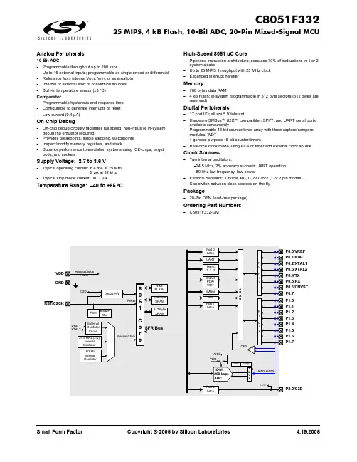
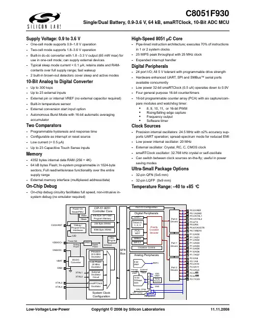
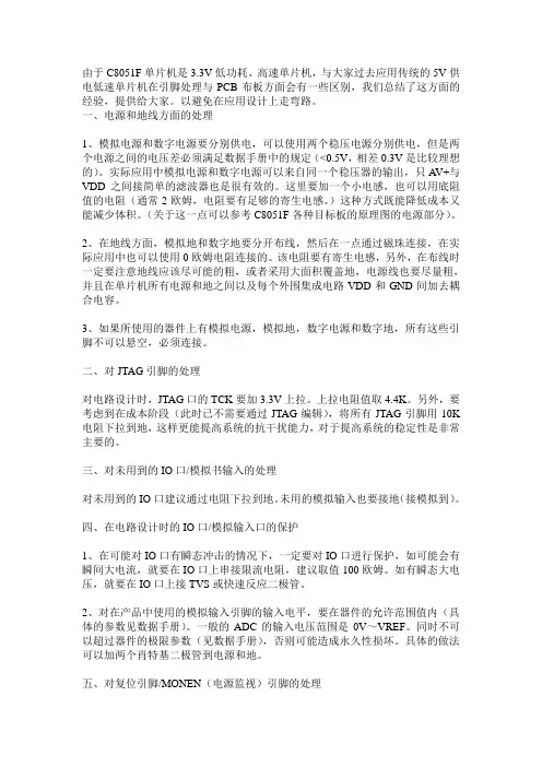
C8051F347_Short
- 格式:pdf
- 大小:403.92 KB
- 文档页数:2
11.97 11.82
47.88 5.91
12.0 12.0
48.0 6.0
12.03 12.18
48.12 6.09
MHz MHz
MHz MHz
Resolution Integral Nonlinearity Differential Nonlinearity Signal-to-Noise Plus Distortion Throughput Rate Input Voltage Range
are reserved)
Digital Peripherals
- 25 port I/O; all are 5 V tolerant - Hardware SMBus™ (I2C™ compatible), SPI™, and UART serial ports
available concurrently
Enable
C2D
Debug HW
RST/C2CK
XTAL1 XTAL2
POR
BrownOut
External Oscillator
Circuit
12 MHz Internal Oscillator
x4
÷2
8
0
5 1 Reset
32 kB FLASH
256 Byte SRAM
2 kB
C
XRAM
o r SFR Bus
Regulator Input Voltage (REGIN) VDD (VREG Output) VREG Bias Current
Supply Current with CPU and USB active
Supply Current (suspend mode, Oscillator off)
Two Comparators
Internal Voltage Reference: 2.4 V
POR/Brown-out Detector
USB Function Controller
- USB specification 2.0 compliant - Full-speed (12 Mbps) or low-speed (1.5 Mbps) operation - Integrated clock recovery; no external crystal required for either full-
pods, and sockets
Temperature Range: –40 to +85 °C
High-Speed 8051 µC Core
- Pipelined instruction architecture; executes 70% of instructions in 1 or 2
system clocks
Selected Electrical Specifications
(TA = 0 to +70 C°, VREG = 5.0 V unless otherwise specified)
Parameter Global Characteristics
Conditions
Min Typ Max Units
C8051F347
USB, 25 MIPS, 32 kB Flash, 10-Bit ADC, 32-Pin Mixed-Signal MCU
Analog Peripherals
10-Bit ADC
- ±1 LSB INL; no missing codes - Programmable throughput up to 200 ksps - Up to 17 external inputs; programmable as single-ended or differential - Built-in temperature sensor (±3 °C)
e System
Clock
D+ D-
VBUS
Clock Recovery
÷2 ÷ 1,2,3,4
USB Clock
USB Transceiver
USB Controller
1 kB USB SRAM
Port 0 Latch
Port 1 Latch
Port 2 Latch
UART0
Timer 0,1,2,3 /
P1.0 P1.1 P1.2 P1.3 P1.4 P1.5 P1.6 P1.7
P2.0 P2.1 P2.2 P2.3 P2.4 P2.5 P2.6 P2.7
P3.0/C2D
USB
Copyright © 2006 by Silicon Laboratories
1.4.2006
C8051F347
USB, 25 MIPS, 32 kB Flash, 10-Bit ADC, 32-Pin Mixed-Signal MCU
- 4 general-purpose 16-bit counter/timers - Programmable 16-bit counter array with 5 capture/compare modules
Clock Sources
- Internal oscillator: 0.25% accuracy with clock recovery enabled;
RTC
PCA/ WDT
SMBus
SPI
P 0
D r v
C
R
P
O
1
S
S
D
B
r
A
v
R
P 2
D r v
Port 3 Latch
VREF
VREF
VDD
10-bit 200 ksps ADC
P 3
D r v
CP0
+
-
CP1
+
-
Temp
A
AIN0-AIN16
M
U VDD
X VREF
P0.0 P0.1 P0.2/XTAL1 P0.3/XTAL2 P0.4 P0.5 P0.6/CNVSTR P0.7/VREF
Comparator
Response Time Mode0 Current Consumption Mode0 Response Time Mode1 Current Consumption Mode1 Response Time Mode2 Current Consumption Mode2 Response Time Mode3 Current Consumption Mode3
speed or low-speed operation
- Supports eight flexible endpoints - Dedicated 1 kB USB buffer memory - Integrated transceiver; no external resistors required
- Up to 25 MIPS throughput with 25 MHz Clock - Expanded interrupt handler
Memory
- 2304 bytes data RAM (256 + 2 kB) - 32 kB Flash; in-system programmable in 512-byte sectors (512 bytes
Operating Voltage: 2.7 to 5.25 V
Package
- 32-Pin LQFP (lead-free package)
Ordering Part Number
- C8051F347-GQ
REGIN
VDD GND
5.0V IN
Voltage
Regulator
OUT
Analog/Digital Power
On-Chip Debug
- On-chip debug circuitry facilitates full speed, non-intrusive in-system
debug (no emulator required)
- Provides breakpoints, single stepping - Inspect/modify memory, registers, and USB memory - Superior performance to emulation systems using ICE-chips, target
Guaranteed Monotonic
(CP+) – (CP-) = 100 mV (CP+) – (CP-) = 100 mV (CP+) – (CP-) = 100 mV (CP+) – (CP-) = 100 mV
10
bits
—
±1/2
±1
LSB
—
±1/2
±1
LSB
51
—
—
dB
—
—
200
ksps
0
—
VREF
V
—0.1— Nhomakorabeaµs
—
7.6
—
µA
—
0.18
—
µs
—
3.2
—
µA
—
0.32
—
µs
—
1.3
—
µA
—
1
—
µs
—
0.4
—
µA
Package Information
C8051F340DK Development Kit
D D1
32 PIN 1 IDENTIFIER 1