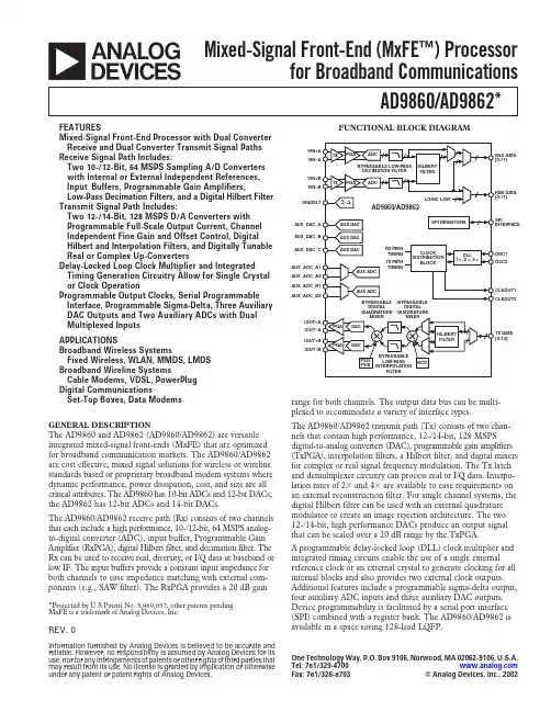
REV.0aInformation furnished by Analog Devices is believed to be accurate and reliable. However, no responsibility is assumed by Analog Devices for its use, nor for any infringements of patents or other rights of third parties that may result from its use. No license is granted by implication or otherwise under any patent or patent rights of Analog Devices.One Technology Way, P.O. Box 9106, Norwood, MA 02062-9106, U.S.A.Tel: 781/ Fax: 781/326-8703© Analog Devices, Inc., 2002AD9860/AD9862*Mixed-Signal Front-End (MxFE ™) Processorfor Broadband Communications*Protected by U.S.Patent No. 5,969,657; other patents pending.MxFE is a trademark of Analog Devices, Inc.GENERAL DESCRIPTIONThe AD9860 and AD9862 (AD9860/AD9862) are versatile integrated mixed-signal front-ends (MxFE) that are optimized for broadband communication markets. The AD9860/AD9862are cost effective, mixed signal solutions for wireless or wireline standards based or proprietary broadband modem systems where dynamic performance, power dissipation, cost, and size are all critical attributes. The AD9860 has 10-bit ADCs and 12-bit DACs;the AD9862 has 12-bit ADCs and 14-bit DACs.The AD9860/AD9862 receive path (Rx) consists of two channels that each include a high performance, 10-/12-bit, 64 MSPS analog-to-digital converter (ADC), input buffer, Programmable Gain Amplifier (RxPGA), digital Hilbert filter, and decimation filter. The Rx can be used to receive real, diversity, or I/Q data at baseband or low IF. The input buffers provide a constant input impedance for both channels to ease impedance matching with external com-ponents (e.g., SAW filter). The RxPGA provides a 20dB gainrange for both channels. The output data bus can be multi-plexed to accommodate a variety of interface types.The AD9860/AD9862 transmit path (Tx) consists of two chan-nels that contain high performance, 12-/14-bit, 128 MSPS digital-to-analog converters (DAC), programmable gain amplifiers (TxPGA), interpolation filters, a Hilbert filter, and digital mixers for complex or real signal frequency modulation. The Tx latch and demultiplexer circuitry can process real or I/Q data. Interpo-lation rates of 2ϫ and 4ϫ are available to ease requirements on an external reconstruction filter. For single channel systems, the digital Hilbert filter can be used with an external quadrature modulator to create an image rejection architecture. The two 12-/14-bit, high performance DACs produce an output signal that can be scaled over a 20 dB range by the TxPGA.A programmable delay-locked loop (DLL) clock multiplier and integrated timing circuits enable the use of a single external reference clock or an external crystal to generate clocking for all internal blocks and also provides two external clock outputs.Additional features include a programmable sigma-delta output,four auxiliary ADC inputs and three auxiliary DAC outputs.Device programmability is facilitated by a serial port interface (SPI) combined with a register bank. The AD9860/AD9862 is available in a space saving 128-lead LQFP.FUNCTIONAL BLOCK DIAGRAMTx DA T A [0:13]SIGDEL T A T A FEATURESMixed-Signal Front-End Processor with Dual Converter Receive and Dual Converter Transmit Signal Paths Receive Signal Path Includes:Two 10-/12-Bit, 64 MSPS Sampling A/D Converters with Internal or External Independent References,Input Buffers, Programmable Gain Amplifiers,Low-Pass Decimation Filters, and a Digital Hilbert Filter Transmit Signal Path Includes:Two 12-/14-Bit, 128 MSPS D/A Converters with Programmable Full-Scale Output Current, Channel Independent Fine Gain and Offset Control, Digital Hilbert and Interpolation Filters, and Digitally Tunable Real or Complex Up-ConvertersDelay-Locked Loop Clock Multiplier and Integrated Timing Generation Circuitry Allow for Single Crystal or Clock OperationProgrammable Output Clocks, Serial Programmable Interface, Programmable Sigma-Delta, Three Auxiliary DAC Outputs and Two Auxiliary ADCs with Dual Multiplexed InputsAPPLICATIONSBroadband Wireless SystemsFixed Wireless, WLAN, MMDS, LMDS Broadband Wireline SystemsCable Modems, VDSL, PowerPlug Digital CommunicationsSet-Top Boxes, Data ModemsAD9860/AD9862–SPECIFICATIONS(V A = 3.3 V ؎ 5%, V D = 3.3 V ؎ 10%, f DAC = 128 MHz, f ADC = 64 MHzNormal Timing Mode, 2؋ DLL Setting, R SET = 4 k⍀, 50 ⍀ DAC Load,–2–REV. 0AD9860/AD9862–3–Test AD9860/AD9862Rx PARAMETERS (continued)Temp Level Min Typ Max Unit DC ACCURACYDifferential Nonlinearity25ºC III±0.3/±0.4LSB Integral Nonlinearity25ºC III±1.2/±5LSB Offset Error25ºC III±0.1%FSR Gain Error25ºC III±0.2%FSR Aperture Delay25ºC III 2.0ns Aperture Uncertainty (Jitter)25ºC III 1.2ps rms Input Referred Noise25ºC III 250µV Reference Voltage ErrorREFT-REFB Error (1 V)25ºC I±1±4mV AD9860 DYNAMIC PERFORMANCE (A IN = –0.5 dBFS, f = 5 MHz)Signal-to-Noise Ratio25∞C I59.0 60.66dBc Signal-to-Noise and Distortion Ratio25∞C I56.0 58.0dBc Total Harmonic Distortion25∞C I–76.5–70.5dBc Spurious Free Dynamic Range25∞C I70.3 81.0dBc AD9862 DYNAMIC PERFORMANCE (A IN = –0.5 dBFS, f = 5 MHz)Signal-to-Noise Ratio25∞C I62.6 64.2dBc Signal-to-Noise and Distortion Ratio25∞C I62.5 64.14dBc Total Harmonic Distortion25∞C I–79.22–73.2dBc Spurious Free Dynamic Range25∞C I77.09 85.13dBc CHANNEL-TO-CHANNEL ISOLATIONTx-to-Rx (A OUT = 0 dBFS, f OUT = 7 MHz)25ºC III >90dB Rx Channel Crosstalk (f1 = 6 MHz, f2 = 9 MHz)25ºC III >80dB PARAMETERSCMOS LOGIC INPUTSLogic “1” Voltage, V IH25ºC II DRVDD – 0.7V Logic “0” Voltage, V IL25ºC II0.4V Logic “1” Current25ºC II12µA Logic “0” Current25ºC II12µA Input Capacitance25ºC III 3pF CMOS LOGIC OUTPUTS (1 mA Load)Logic “1” Voltage, V OH25ºC II DRVDD – 0.6V Logic “0” Voltage, V OL25ºC II0.4V POWER SUPPLYAnalog Supply CurrentsTx (Both Channels, 20 mA FS Output)25ºC I 7076mA Tx Powered Down25ºC I 2.5 5.0mA Rx (Both Channels, Input Buffer Enabled)25ºC I 275307mA Rx (Both Channels, Input Buffer Disabled)25ºC III 245mA Rx (32 MSPS, Low Power Mode, Buffer Disabled)25ºC III 155mA Rx (16 MSPS, Low Power Mode, Buffer Disabled)25ºC III 80mA Rx Path Powered Down25ºC I 5.0 6.0mA DLL25ºC III 12mA Digital Supply CurrentAD9860 Both Rx and Tx Path (All Channels Enabled)2ϫ Interpolation, f DAC = f ADC = 64 MSPS25ºC I 92112mA AD9862 Both Rx and Tx Path (All Channels Enabled)2ϫ Interpolation, f DAC = f ADC = 64 MSPS25ºC I 104124mA Tx Path (f DAC = 128 MSPS)Processing Blocks Disabled25ºC III 45mA 4ϫ Interpolation25ºC III 90mA 4ϫ Interpolation, Coarse Modulation25ºC III 110mA 4ϫ Interpolation, Fine Modulation25ºC III 110mA 4ϫ Interpolation, Coarse and Fine Modulation25ºC III 130mAREV. 0REV. 0–4–AD9860/AD9862Test AD9860/AD9862(20 pF Load)Temp Level Min Typ MaxUnit Minimum Reset Pulsewidth Low (t RL )NA NA 5Clock Cycles Digital Output Rise/Fall Time 25ºC III 2.84ns DLL Output Clock25ºC III 32128MHz DLL Output Duty Cycle25ºC III 50%Tx –/Rx –Interface (See Figures 11 and 12)TxSYNC/TxIQ Setup Time (t Tx1, t Tx3)25ºC III 3ns TxSYNC/TxIQ Hold Time (t Tx2, t Tx4)25ºC III 3ns RxSYNC/RxIQ/IF to Valid Time(t Rx1, t Rx3)25ºC III 5.2ns RxSYNC/RxIQ/IF Hold Time (t Rx2, t Rx4)25ºC III 0.2ns Serial Control Bus (See Figures 1 and 2)Maximum SCLK Frequency (f SCLK )Full III 16MHz Minimum Clock Pulsewidth High (t HI )Full III 30ns Minimum Clock Pulsewidth Low (t LOW )Full III 30ns Maximum Clock Rise/Fall TimeFull III 1ms Minimum Data/SEN Setup Time (t S )Full III 25ns Minimum SEN/Data Hold Time (t H )Full III 0ns Minimum Data/SCLK Setup Time (t DS )Full III 25ns Minimum Data Hold Time (t DH )Full III 0ns Output Data Valid/SCLK Time (t DV )Full III 30ns AUXILARY ADC Conversion Rate 25ºC III 1.25MHz Input Range 25ºC III 3V Resolution 25ºC III 10Bits AUXILARY DAC Settling Time 25ºC III 8m s Output Range 25ºC III 3V Resolution25ºC III 8Bits ADC TIMINGLatency (All Digital Processing Blocks Disabled)25ºC III 7Cycles DAC TimingLatency (All Digital Processing Blocks Disabled)25ºC III 3Cycles Latency (2ϫ Interpolation Enabled)25ºC III 30Cycles Latency (4ϫ Interpolation Enabled)25ºC III 72Cycles Additional Latency (Hilbert Filter Enabled)25ºC III 36Cycles Additional Latency (Coarse Modulation Enabled)25ºC III 5Cycles Additional Latency (Fine Modulation Enabled)25ºC III 8Cycles Output Settling Time (TST) (to 0.1%)25ºCIII35nsSpecifications subject to change without notice.TIMING CHARACTERISTICSTest AD9860/AD9862PARAMETERS (continued)TempLevelMinTyp MaxUnitPOWER SUPPLY (continued)Rx Path (f ADC = 64 MSPS)Processing Blocks Disabled 25ºCIII 9mA Decimation Filter Enabled 25ºC III 15mA Hilbert Filter Enabled25ºC III 16mA Hilbert and Decimation Filter Enabled25ºC III 18.5mANOTES 1% f DATA refers to the input data rate of the digital block.2Interpolation filter stop band is defined by image suppression of 50 dB or greater.Specifications subject to change without notice.REV. 0AD9860/AD9862–5–CAUTIONESD (electrostatic discharge) sensitive device. Electrostatic charges as high as 4000V readily accumulate on the human body and test equipment and can discharge without detection. Although the AD9860/AD9862 features proprietary ESD protection circuitry, permanent damage may occur on devices subjected to high energy electrostatic discharges. Therefore, proper ESD precautions arerecommended to avoid performance degradation or loss of functionality.ABSOLUTE MAXIMUM RATINGS 1Power Supply (V AS , V DS ) . . . . . . . . . . . . . . . . . . . . . . . . .3.9 V Digital Output Current . . . . . . . . . . . . . . . . . . . . . . . . . .5 mA Digital Inputs . . . . . . . . . . . . . . . .–0.3 V to DRVDD + 0.3 V Analog Inputs . . . . . . . . . . . . . .–0.3 V to AVDD (IQ) + 0.3 V Operating Temperature 2 . . . . . . . . . . . . . . . . .–40؇C to +70؇C Maximum Junction Temperature . . . . . . . . . . . . . . . . .150؇C Storage Temperature . . . . . . . . . . . . . . . . . . .–65؇C to +150؇C Lead Temperature (Soldering 10 sec) . . . . . . . . . . . . . .300؇CNOTES 1Absolute maximum ratings are limiting values, to be applied individually, and beyond which the serviceability of the circuit may be impaired. Functional operability under any of these conditions is not necessarily implied. Exposure to absolute maximum rating conditions for extended periods of time may affect device reliability.2The AD9860/AD9862 have been characterized to operate over the industrial temperature range (–40؇C to +85؇C) when operated in Half Duplex Mode.EXPLANATION OF TEST LEVELSI.Devices are 100% production tested at 25ºC and guaranteed by design and characterization testing for the extended industrial temperature range (–40ºC to +70ºC).II.Parameter is guaranteed by design and/or characterization testing.III.Parameter is a typical value only.NA.Test level definition is not applicable.THERMAL CHARACTERISTICS Thermal Resistance128-Lead LQFP JA = 29ºC/WORDERING GUIDEModel Temperature Range Package DescriptionPackage Option AD9860BST –40∞C to +70∞C *128-Lead Low Profile Plastic Quad Flatpack (LQFP) ST-128B AD9862BST –40∞C to +70∞C *128-Lead Low Profile Plastic Quad Flatpack (LQFP) ST-128BAD9860PCB Evaluation Board with AD9860AD9862PCBEvaluation Board with AD9862*The AD9860/AD9862 have been characterized to operate over the industrial temperature range (–40؇C to +85؇C) when operated in Half Duplex Mode.REV. 0–6–AD9860/AD9862PIN CONFIGURATIONAGND AVDD DVDD DGND DGND DVDD Tx11/13 (MSB)Tx10/12T x 9/1T x 8/1T x 7/T x 6/T x 5/T x 4/T x 3/T x 2/T x 1/T x 0/N C /T x N C /T x AUX_ADC_A1AGND AVDD AVDD SIGDEL T AUX_DAC_A AUX_DAC_B AUX_DAC_CAGNDDLL_Lock AGND NC AVDD OSC1OSC2AGND CLKSEL AVDD AGND AVDD REFIO FSADJ AVDD AGND IOUT–A IOUT+A AGND AGND IOUT+B IOUT–B T x S Y N D G N D V D S C L S D S D I S E D G N D V D D G N D V D M O D E /T x B L A N R E S E T C L K O U T A G N DA V D DA V D DA G N DV I N +BV I N –BA G N DA G N DV R E FA G N DA G N DV I N –AV I N +AA G N DA V D DA V D DA G N DR E F B _AR E F T _AA G N DA V D DA V D DA U X _A D C _B 2A U X _A D C _B 1A U X _A D C _R E FA U X _A D C _A 2NC = NO CONNECTAD9860/AD9862–7–Pin No.Mnemonic FunctionClock Pins10DLL_Lock DLL Lock Indicator Pin11, 16AGND DLL Analog Ground Pins12NC No Connect13AVDD DLL Analog Supply Pin14OSC1Single Ended Input Clock(or Crystal Oscillator Input)15OSC2Crystal Oscillator Input17CLKSEL Controls CLKOUT1 Rate64CLKOUT2Clock Output Generated from InputClock (DLL Multiplier Settingand CLKOUT2 Divide Factor)65CLKOUT1Clock Output Generated fromInput Clock (1ϫ if CLKSEL = 1or /2 if CLKSEL = 0)Various Pins1AUX_ADC_A1Auxiliary ADC A Input 13, 4, 13AVDD Analog Power Pins2, 9AGND Analog Ground Pins5SIGDELT Digital Output fromProgrammable Sigma-Delta6AUX_DAC_A Auxiliary DAC A Output7AUX_DAC_B Auxiliary DAC B Output8AUX_DAC_C Auxiliary DAC C Output33, 36, 53,DVDD Digital Power Supply Pin59, 61, 66,9334, 35, 52,DGND Digital Ground Pin58, 60, 67,9454SCLK Serial Bus Clock Input55SDO Serial Bus Data Bit56SDIO Serial Bus Data Bit57SEN Serial Bus Enable63RESETB Reset (SPI Registers and Logic) 95AUX_SPI_do Optional Auxiliary ADC Serial BusData Out Bit96AUX_SPI_clk Optional Auxiliary ADC Serial BusData Out Latch Clock97AUX_SPI_csb Optional Auxiliary ADC Serial BusChip Select Bit128AUX_ADC_A2Auxiliary ADC A Input 2126AUX_ADC_B1Auxiliary ADC B Input 1125AUX_ADC_B2Auxiliary ADC B Input 2127AUX_ADC_REF Auxiliary ADC ReferencePin No.Mnemonic FunctionReceive Pins68/70–79D0A to10-/12-Bit ADC Output ofD9A/D11A Receive Channel A80/82–91D0B to10-/12-Bit ADC Output ofD9B/D11B Receive Channel B92RxSYNC Synchronization Clock forChannel A and Channel B Rx Paths98, 99,AVDD Analog Supply Pins104, 105,117, 118,123, 124,100, 103,AGND Analog Ground Pins106, 109,110, 112,113, 116,119, 122,101REFT_B Top Reference Decoupling forChannel B ADC102REFB_B Bottom Reference Decouplingfor Channel B ADC107VIN+B Receive Channel B Differential (+) Input108VIN–B Receive Channel B Differential (؊) Input111VREF Internal ADC Voltage Reference114VIN–A Receive Channel A Differential (؊) Input115VIN+A Receive Channel A Differential (+) Input120REFB_A Bottom Reference Decoupling forChannel A ADC121REFT_A Top Reference Decoupling forChannel A ADCTransmit Pins18, 20AVDD Analog Supply Pins23, 3219, 24,AGND Analog Ground Pins27, 28, 3121REFIO Reference Output, 1.2 V Nominal22FSADJ Full-Scale Current Adjust25IOUT–A Transmit Channel A DACDifferential (؊) Output26IOUT+A Transmit Channel A DACDifferential (+) Output29IOUT+B Transmit Channel B DACDifferential (+) Output30IOUT–B Transmit Channel B DACDifferential (؊) Output37–48/50Tx11/Tx1312-/14-Bit Transmit DAC Datato Tx0(Interleaved Data when Required)51TxSYNC Synchronization Input for Transmitter62MODE/Configures Default Timing Mode,TxBLANK*Controls Tx Digital Power Down*The logic level of the Mode/TxBLANK pin at power up defines the default timingmode; a logic low configures Normal Operation, logic high configures AlternateOperation Mode.PIN FUNCTION DESCRIPTIONSREV. 0AD9860/AD9862DEFINITIONS OF SPECIFICATIONSDifferential Nonlinearity Error (DNL, No Missing Codes)An ideal converter exhibits code transitions that are exactly 1LSB apart. DNL is the deviation from this ideal value. Guaranteed no missing codes to 10-bit resolution indicate that all 1024 codes respectively, must be present over all operating ranges.Integral Nonlinearity Error (INL)Linearity error refers to the deviation of each individual code from a line drawn from “negative full scale” through “positive full scale.” The point used as “negative full scale” occurs 1/2LSB before the first code transition. “Positive full scale” is defined as a level 1 1/2 LSB beyond the last code transition. The deviation is measured from the middle of each particular code to the true straight line.Phase NoiseSingle-sideband phase noise power is specified relative to the carrier (dBc/Hz) at a given frequency offset (1 kHz) from the carrier. Phase noise can be measured directly in Single Tone Trans-mit Mode with a spectrum analyzer that supports noise marker measurements. It detects the relative power between the carrier and the offset (1 kHz) sideband noise and takes the resolution bandwidth (rbw) into account by subtracting 10 log(rbw). It also adds a correction factor that compensates for the implementation of the resolution bandwidth, log display, and detector characteristic. Output Compliance RangeThe range of allowable voltage at the output of a current-output DAC. Operation beyond the maximum compliance limits may cause either output stage saturation or breakdown, resulting in nonlinear performance.Spurious-Free Dynamic Range (SFDR)The difference, in dB, between the rms amplitude of the DAC’s output signal (or ADC’s input signal) and the peak spurious signal over the specified bandwidth (Nyquist bandwidth unless otherwise noted).Pipeline Delay (Latency)The number of clock cycles between conversion initiation and the associated output data being made available.Offset ErrorFirst transition should occur for an analog value 1/2 LSB above –full scale. Offset error is defined as the deviation of the actual transition from that point.Gain ErrorThe first code transition should occur at an analog value 1/2LSB above –full scale. The last transition should occur for an analog value 1 1/2 LSB below the nominal full scale. Gain error is the deviation of the actual difference between first and last code transitions and the ideal difference between first and last code transitions.Aperture DelayThe aperture delay is a measure of the Sample-and-Hold Ampli-fier (SHA) performance and specifies the time delay between the rising edge of the sampling clock input to when the input signal is held for conversion.Aperture Uncertainty (Jitter)Aperture jitter is the variation in aperture delay for successivesamples and is manifested as noise on the input to the ADC.Input Referred NoiseThe rms output noise is measured using histogram techniques.The ADC output code’s standard deviation is calculated in LSB and converted to an equivalent voltage. This results in a noisefigure that can be referred directly to the input of the AD9860/ AD9862.Signal-to-Noise and Distortion (S/N+D, SINAD) RatioS/N+D is the ratio of the rms value of the measured input signal to the rms sum of all other spectral components below the Nyquist frequency, including harmonics but excluding dc. The value for S/N+D is expressed in decibels.Effective Number of Bits (ENOB)For a sine wave, SINAD can be expressed in terms of the number of bits. Using the following formula:N=()SINAD dB–..176602it is possible to get a measure of performance expressed as N,the effective number of bits. Thus, effective number of bits fora device for sine wave inputs at a given input frequency can becalculated directly from its measured SINAD.Signal-to-Noise Ratio (SNR)SNR is the ratio of the rms value of the measured input signal to the rms sum of all other spectral components below the Nyquist frequency, excluding harmonics and dc. The value for SNR isexpressed in decibels.Total Harmonic Distortion (THD)THD is the ratio of the rms sum of the first six harmoniccomponents to the rms value of the measured input signal and is expressed as a percentage or in decibels.Power Supply RejectionPower supply rejection specifies the converter’s maximum full-scale change when the supplies are varied from nominal to minimum and maximum specified voltages.Channel-to-Channel Isolation (Crosstalk)In an ideal multichannel system, the signal in one channel will not influence the signal level of another channel. The channel-to-channel isolation specification is a measure of the change that occurs to a grounded channel as a full-scale signal is applied to another channel.REV. 0–8––9–FREQUENCY – MHzTPC 1.AD9862 Tx Output 6 MHzSingle Tone; CLKIN = 32 MHz;DLL 4ϫ SettingFREQUENCY – MHzMAGNITUDE–dBm–20–4020406080100110120–60–80140TPC 4.TxDAC Generating anOFDM Signal; CLKIN = 64 MHz,DLL 2ϫ Settingf OUT – MHz5203510152530THD–dBcTPC 7.TxDAC HarmonicDistortion vs. f OUTFREQUENCY – MHzTPC 2.AD9862 Tx Output 6 MHzSingle Tone; CLKIN = 64 MHz;DLL 2ϫ SettingFREQUENCY – MHzMAGNITUDE–dBm20406080100110120140TPC 5.TxDAC Generating anOFDM Signal; CLKIN = 64 MHz,DLL 2ϫ SettingFREQUENCY– MHzSNR–dB74737271706968TPC 8.Signal-to-Noise Ratio (SNR)vs. f OUTFREQUENCY – MHzTPC 3.AD9862 Tx Output 6 MHzSingle Tone; CLKIN = 128 MHz;DLL 1ϫ SettingFREQUENCY – MHzMAGNITUDE–dBm–20–40–60–80–100–120TPC 6.Zoomed in Plot of FourNotched Carriers of OFDM Signal;CLKIN = 64 MHz, DLL 2ϫ SettingCARRIER FREQUENCY – MHz5IMD–dBc20–60–65–70–75–80–85–9010152530–50–55–95TPC 9.Two Tone Intermodulationvs. f OUT1 (f OUT2 = f OUT1 + 1 MHz)REV. 0AD9860/AD9862FFT OUTPUT – MHz5FFTMAGNITUDE–dBFS20–20–40–60–8010152530–100–120TPC 10.ADC Dual Tone FFT withBuffer Tones at 4.5 MHz and 5.5 MHzf IN – MHz52TPC 13.AD9862 Rx SINADvs. fINat 64 MSPSf IN – MHzTPC 16.AD9860 Rx SINADvs. f IN at 64 MSPSFFT OUTPUT – MHz5FFTMAGNITUDE–dBFS20–20–40–60–8010152530–100–120TPC 11.ADC Dual Tone FFT withoutBuffer Tones at 4.5 MHz and 5.5 MHzf IN – MHzSINAD–dBcTPC 14.AD9862 Rx SINADvs. f IN at 32 MSPSf IN – MHzSINAD–dBc62TPC 17.AD9860 Rx SINADvs. f IN at 32 MSPSFFT OUTPUT – MHz5FFTMAGNITUDE–dBFS20–20–40–60–8010152530–100–120TPC 12.ADC Dual Tone FFT(undersampling) without BufferTones at 69.5 MHz and 70.5 MHzf IN – MHz020050SINAD–dBc150250100300TPC 15.AD9862 Rx SINADvs. f IN at 16 MSPSf IN – MHzSINAD–dBc62TPC 18.AD9860 Rx SINADvs. f IN at 16 MSPSREV. 0–10–AD9860/AD9862INPUT FREQUENCY – MHzT H D – d B c–60–65–70–75–80–85–90–50–55–95–100TPC 19.Rx THD vs. f IN ,F ADC = 64 MSPSINPUT FREQUENCY – MHzS F D R – d B c–60–65–70–75–80–85–90–50–55–95–100TPC 22.Rx SFDR @ 64 MSPSINPUT FREQUENCY – MHzR E L A T I V E A T T E N U A T I O N – d B10–1–2–3–4–5–6TPC 25.Rx Input Attenuationf IN – MHzT H D – d B c–75–80–85–90–70–65–60–55–50TPC 20.Rx THD vs. f IN ,F ADC = 32 MSPS f IN – MHzS F D R – d B c–75–80–85–90–70–65–60–55–50–95TPC 23.Rx SFDR @ 32 MSPS f IN – MHzI N P U T I M P E D A N C E – ⍀60250240230220210200190204080100270260180280TPC 26.Rx Input Buffer Impedance vs. f INf IN – MHzT H D – d B c–75–80–85–90–70–65–60–55–50TPC 21.Rx THD vs. f IN ,F ADC = 16 MSPSf IN – MHz020050S F D R – d B c–75–80–85–90–70150250100–65–60–55–50300–95TPC 24.Rx SFDR @ 16 MSPSf ADC – MSPS04010R x A N A L O G P O W E R – m W30020010004003050205006007008007060TPC 27.Rx Analog Power ConsumptionAD9860/AD9862REGISTER MAP (0x00–0x3F)1NOTES1When writing to a register with unassigned register bit(s), a logic low must be written to the unassigned bit(s). By default, after power up or RESET, all registers are set low, except for the bits in the shaded boxes, which are set high.2DecimalAD9860/AD9862REGISTER BIT DEFINITIONSREGISTER 0: GENERALBIT 7: SDIO BiDir (Bidirectional)Default setting is low, which indicates SPI serial port uses dedi-cated input and output lines (i.e., 4-wire interface), SDIO and SDO Pins, respectively. Setting this bit high configures the serial port to use the SDIO Pin as a bidirectional data pin.BIT 6: LSB FirstDefault setting is low, which indicates MSB first SPI Port Access Mode. Setting this bit high configures the SPI port access to LSB first mode.BIT 5: Soft ResetWriting a high to this register resets all the registers to their default values and forces the DLL to relock to the input clock. The Soft Reset Bit is a one shot register and is cleared immediately after the register write is completed.REGISTER 1: Rx PWRDWNBIT 7: V REF, diff (Power-Down)Setting this bit high will power down the ADC’s differential references (i.e., REFT and REFB).BIT 6: V REF (Power-Down)Setting this register bit high will power down the ADC reference circuit (i.e., V REF).BIT 5: Rx Digital (Power-Down)Setting this bit high will power down the digital section of the receive path of the chip. Typically, any unused digital blocks are automatically powered down.BIT 4/3: Rx Channel B/Rx Channel A (Power-Down)Either ADC or both ADCs can be powered down by setting the appropriate register bit high. The entire Rx channel is powered down, including the differential references, input buffer, and the internal digital block. The bandgap reference remains active for quick recovery.BIT 2/1: Buffer B/Buffer A (Power-Down)Setting either of these bits high will power down the input buffer circuits for the respective channel. The input buffer should be powered down when bypassed. By default, these bits are low and the input buffers are enabled.BIT 0: All Rx (Power-Down)Setting this bit high powers down all circuits related to the receive path.REGISTER 2/3: Rx A/Rx BBIT 7: Bypass Buffer A/Bypass Buffer BSetting either of these bits high will bypass the respective input buf-fer circuit. When the buffer is bypassed, the input signal is routed directly to the switched capacitor SHA input of the RxPGA. When operating with buffer bypassed, it should be powered down.BIT 0–4: RxPGA A/RxPGA BThese 5-bit straight binary registers (Bit 0 is the LSB, Bit 4 is the MSB) provide control for the programmable gain amplifiers in the dual receive paths. A 0 dB to 20 dB gain range is accom-plished through a switched capacitor network with fast settling of a few clock cycles. The step size is approximately 1 dB. The register default setting is minimum gain or hex00. The maximum setting for these registers is hex14.REGISTER 4: Rx MISCBIT 2: HS (High Speed) Duty CycleSetting this bit high optimizes duty cycle of the internal ADC sampling clock. It is recommended that this bit be set high in high speed applications when clock duty cycle affects noise and distortion performance the most. This bit should be set high in conjunction with Clk Dut Enable register bit.BIT 1: Shared RefSetting this bit high forces the dual receive ADCs into a mode to share their differential references to provide superior gain matching. When this option is enabled, the REFT of Channel A and Channel B should be connected together off-chip and the REFB of both channels should be connected.BIT 0: Clk DutySetting this bit high enables an on-chip duty cycle stabilizer (DCS) circuit to generate the internal clock for the Rx block. This option is useful for adjusting for high speed input clocks with skewed duty cycle. The DCS Mode can be used with ADC sampling frequencies over 40 MHz.REGISTER 5: Rx I/F (INTERFACE)BIT 4: Three-stateSetting this bit high will force both Rx data output buses, including the RxSYNC Pin, into a three-state mode.BIT 3: Rx RetimeThe Rx path can use either of the clock outputs, CLKOUT1 or CLKOUT2, to latch the Rx output data. Since CLKOUT1 and CLKOUT2 have slight phase offsets, this provides some timing flexibility with the interface. By default, this bit is low and the Rx output latches use CLKOUT1. Setting this bit will force the Rx output latches to use CLKOUT2.BIT 2: Twos ComplementDefault data format for the Rx data is straight binary. Setting this bit high will generate two’s complement data.BIT 1: Inv RxSyncWhen the receive data is multiplexed onto one data port (i.e., Mux Mode Enabled), the RxSYNC Pin can be used to decode which channel generated the current output data at the active port. Default condition is that RxSYNC is high when Channel A is at the output and is low when Channel B is at the output. Setting this bit high reverses this synchronization.BIT 0: Mux OutSetting this bit high enables the Rx Mux Mode. Default setting is low, which is Dual Port Mode, (i.e., non Rx Mux Mode). When in Rx Mux Mode, both Rx channels share the same output data bus, pins D0A to D9A (for AD9860) or D0A to D11A (for AD9862). The other Rx output bus (pins D0B to D9B or D0B to D11B) outputs a low logic.REGISTER 6: Rx DigitalBIT 3: 2 ChannelSetting this bit low disables the Rx B output data port (pins D0B to D9B or D11B), forcing the output pins to zero. By default, the bit is high and both data paths are active.BIT 2: Keep –veThis bit selects whether the receive Hilbert filter will filter positive or negative frequencies, assuming the filter is enabled. By default this bit is low, which passes positive frequencies. Setting this bit high will configure the filter to pass negative frequencies.BIT 1: HilbertThis bit enables or disables the Hilbert filter in the receive path. By default, this bit is low, which disables the receive Hilbert filter. Setting this bit high enables the receive Hilbert filter.BIT 0: DecimateThis register enables or disables the decimation filters. By default, the register setting is low and the decimation filter is disabled.。