MAX4622CSE中文资料
- 格式:pdf
- 大小:171.76 KB
- 文档页数:12
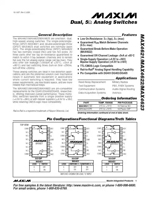
For free samples & the latest literature: , or phone 1-800-998-8800.For small orders, phone 1-800-835-8769.General DescriptionThe MAX4621/MAX4622/MAX4623 are precision, dual,high-speed analog switches. The single-pole/single-throw (SPST) MAX4621 and double-pole/single-throw (DPST) MAX4623 dual switches are normally open (NO). The single-pole/double-throw (SPDT) MAX4622has two normally closed (NC) and two NO poles. All three parts offer low 5Ωon-resistance guaranteed to match to within 0.5Ωbetween channels and to remain flat over the full analog signal range (∆0.5Ωmax).They also offer low leakage (<500pA at +25°C, <5nA at +85°C) and fast switching times (turn-on time <250ns,turn-off time <200ns).These analog switches are ideal in low-distortion appli-cations and are the preferred solution over mechanical relays in automatic test equipment or applications where current switching is required.They have low power requirements, use less board space, and are more reliable than mechanical relays.The MAX4621/MAX4622/MAX4623 are pin-compatible replacements for the DG401/DG403/DG405, respective-ly, offering improved overall performance. These mono-lithic switches operate from a single positive supply (+4.5V to +36V) or with bipolar supplies (±4.5V to ±18V)while retaining CMOS-logic input compatibility.Featureso Low On-Resistance: 3Ω(typ), 5Ω(max)o Guaranteed R ON Match Between Channels (0.5Ωmax)o Guaranteed Break-Before-Make Operation (MAX4622)o Guaranteed Off-Channel Leakage <5nA at +85°C o Single-Supply Operation (+4.5V to +36V)Bipolar-Supply Operation (±4.5V to ±18V)o TTL/CMOS-Logic Compatibleo Rail-to-Rail ®Analog Signal Handling Capability o Pin Compatible with DG401/DG403/DG405ApplicationsReed Relay Replacement Military Radios Test EquipmentPBX, PABX Systems Communication Systems Audio-Signal Routing Data-Acquisition SystemsAvionicsMAX4621/MAX4622/MAX4623Dual, 5ΩAnalog Switches________________________________________________________________Maxim Integrated Products119-1497; Rev 0; 8/99Ordering Information continued at end of data sheet.Pin Configurations/Functional Diagrams/Truth TablesOrdering InformationRail-to-Rail is a registered trademark of Nippon Motorola, Ltd.M A X 4621/M A X 4622/M A X 4623Dual, 5ΩAnalog Switches 2_______________________________________________________________________________________ABSOLUTE MAXIMUM RATINGSELECTRICAL CHARACTERISTICS—Dual Supplies(V+ = +15V, V- = -15V, V L = +5V, GND = 0, V INH = +2.4V, V INL = +0.8V, T A = T MIN to T MAX , unless otherwise noted. Typical values are at T A = +25°C.) (Note 2)Stresses beyond those listed under “Absolute Maximum Ratings” may cause permanent damage to the device. These are stress ratings only, and functional operation of the device at these or any other conditions beyond those indicated in the operational sections of the specifications is not implied. Exposure to absolute maximum rating conditions for extended periods may affect device reliability.(Voltages Referenced to GND)V+ to GND..............................................................-0.3V to +44V V- to GND...............................................................+0.3V to -44V V+ to V-...................................................................-0.3V to +44V V L to GND.....................................................-0.3V to (V+ + 0.3V)All Other Pins to GND (Note 1) ...........(V- - 0.3V) to (V+ + 0.3V)Continuous Current (COM_, NO_, NC_) ........................±100mA Peak Current (COM_, NO_, NC_)(pulsed at 1ms, 10% duty cycle) ...............................±300mAContinuous Power Dissipation (T A = +70°C)Narrow SO (derate 8.70mW/°C above +70°C).............696mW Narrow DIP (derate 10.53mW/°C above +70°C)..........842mW Operating Temperature RangesMAX462_C_ _......................................................0°C to +70°C MAX462_E_ _....................................................-40°C to +85°C Storage Temperature Range.............................-65°C to +150°C Lead Temperature (soldering, 10sec).............................+300°CNote 1:Signals on NO_, NC_, or COM_ exceeding V+ or V- are clamped by internal diodes. Limit forward-diode current to maxi-mum current rating.ELECTRICAL CHARACTERISTICS—Dual Supplies (continued)MAX4621/MAX4622/MAX4623Dual, 5ΩAnalog Switches (V+ = +15V, V- = -15V, V L= +5V, GND = 0, V INH= +2.4V, V INL= +0.8V, T A= T MIN to T MAX, unless otherwise noted. Typical valuesare at T A= +25°C.) (Note 2)M A X 4621/M A X 4622/M A X 4623Dual, 5ΩAnalog Switches 4_______________________________________________________________________________________ELECTRICAL CHARACTERISTICS—Single Supply(V+ = +12V, V- = 0, V L = +5V, GND = 0, V INH = +2.4V, V INL = +0.8V, T A = T MIN to T MAX , unless otherwise noted. Typical values are T A = +25°C.) (Note 2)MAX4621/MAX4622/MAX4623Dual, 5ΩAnalog Switches_______________________________________________________________________________________5Note 2:The algebraic convention, where the most negative value is a minimum and the most positive value is a maximum, is usedin this data sheet.Note 3:Guaranteed by design.Note 4:∆R ON = R ON_MAX - R ON_MIN .Note 5:Flatness is defined as the difference between the maximum and minimum values of on-resistance as measured over thespecified analog signal range.Note 6:Leakage currents are 100% tested at the maximum-rated hot temperature and guaranteed by correlation at +25°C.Note 7:Off-isolation = 20log 10[V COM_ / (V NC_or V NO_)]. V COM_= output, V NC_or V NO_= input to off switch.Note 8:Between any two switches.Note 9:Leakage testing for single-supply operation is guaranteed by testing with dual supplies.ELECTRICAL CHARACTERISTICS—Single Supply (continued)(V+ = +12V, V- = 0, V L = +5V, GND = 0, V INH = +2.4V, V INL = +0.8V, T A = T MIN to T MAX , unless otherwise noted. Typical values are T A = +25°C.) (Note 2)M A X 4621/M A X 4622/M A X 4623Dual, 5ΩAnalog Switches 6_______________________________________________________________________________________Typical Operating Characteristics(T A = +25°C, unless otherwise noted.)2.03.02.54.03.55.04.55.56.56.07.0-20-10-5-1505101520ON-RESISTANCEV COM (V)R O N (Ω)1.52.52.03.53.04.54.05.0-15-50-1051015ON-RESISTANCE vs. V COMAND TEMPERATURE (DUAL SUPPLIES)V COM (V)R O N (Ω)264108121416186931215182124ON-RESISTANCEvs. V COM (SINGLE SUPPLY)V COM (V)R O N (Ω)3.04.54.03.55.05.56.06.57.07.58.0042681012ON-RESISTANCE vs. V COMAND TEMPERATURE (SINGLE SUPPLY)V COM (V)R O N (Ω)0.010.110k 1011001k 0.001-40-10520-253550958065SUPPLY CURRENT vs. TEMPERATURETEMPERATURE (°C)I +, I - (n A )1010.11001k 10k -40-10520-253550958065ON/OFF-LEAKAGE CURRENTvs. TEMPERATURETEMPERATURE (°C)L E A K A G E (p A )0.010-100100-200300200500400600700-15-5-10051015CHARGE INJECTION vs. V COMV COM (V)Q (p C )-10-1000.1100101FREQUENCY RESPONSE-70-90-30-500-60-80-20-40FREQUENCY (MHz)L O S S (d B )90180-720-450-630-90-270-360-5400-180P H A S E (D E G R E E S )Pin Description Applications InformationMAX4621/MAX4622/MAX4623Dual, 5ΩAnalog SwitchesOperation with Supply Voltages Array Other than ±15VThe MAX4621/MAX4622/MAX4623 switches operate with±4.5V to ±18V bipolar supplies and a +4.5V to +36V sin-gle supply. In either case, analog signals ranging fromV+ to V- can be switched. The Typical OperatingCharacteristics graphs show the typical on-resistancevariation with analog signal and supply voltage.Overvoltage ProtectionProper power-supply sequencing is recommended for allCMOS devices. It is important not to exceed the absolutemaximum ratings because stresses beyond the listed rat-ings may cause permanent damage to the devices.Always sequence V+ on first, followed by V L, V-, andlogic inputs. If power-supply sequencing is not possible,add two small signal diodes in series with the supply pinsand a Schottky diode between V+ and V L(Figure 1).Adding diodes reduces the analog signal range to 1Vbelow V+ and 1V above V-, but low switch resistance andlow leakage characteristics are unaffected. The differ-ence between V+ and V- should not exceed +44V.Figure 1. Overvoltage Protection Using Blocking Diodes_______________________________________________________________________________________7M A X 4621/M A X 4622/M A X 4623Dual, 5ΩAnalog Switches 8_______________________________________________________________________________________Figure 2. Switching-Time Test CircuitFigure 3. MAX4622 Break-Before-Make Test CircuitFigure 4. Charge-Injection Test CircuitMAX4621/MAX4622/MAX4623Dual, 5ΩAnalog Switches_______________________________________________________________________________________9Figure 5. Off-IsolationFigure 6. Crosstalk Test CircuitFigure 8. Channel-Off CapacitanceFigure 7. Channel-On CapacitanceM A X 4621/M A X 4622/M A X 4623Dual, 5ΩAnalog Switches 10______________________________________________________________________________________Ordering Information (continued)Chip InformationPackage InformationTRANSISTOR COUNT: 82Package Information (continued)MAX4621/MAX4622/MAX4623Dual, 5ΩAnalog Switches Array______________________________________________________________________________________11M A X 4621/M A X 4622/M A X 4623Dual, 5ΩAnalog Switchesimplied. Maxim reserves the right to change the circuitry and specifications without notice at any time.Maxim cannot assume responsibility for use of any circuitry other than circuitry entirely embodied in a Maxim product. No circuit patent licenses are 12____________________Maxim Integrated Products, 120 San Gabriel Drive, Sunnyvale, CA 94086 408-737-7600©1999 Maxim Integrated Products Printed USA is a registered trademark of Maxim Integrated Products.NOTES。