FW Module Test Introduction(LCD&Touch)
- 格式:ppt
- 大小:928.00 KB
- 文档页数:16


实验十三字符LCD 显示实验一、实验目的1、了解字符LCD 模块的使用方法2、掌握8051 单片机控制字符LCD 模块显示程序的设计方法。
二、实验原理字符LCD 模块是一种专用显示字符、数字或符号的液晶显示模块。
这种模块每一个符号由5×7、5×8 或5×11 的点阵像素排列组成的,字符间隔为一个点距,行间隔为一个行距,模块本身附有显示驱动控制电路,可以与单片机的I/O 口线直接连接,使用方便。
目前广泛使用的字符LCD 模块其显示驱动控制电路多是HD44780 或兼容品,其接口信号、操作指令相同。
本实验选用的字符LCD 模块是香港精电公司生产的规格为16×1 的字符LCD 模块,可以在一行上显示16 个字符。
该模块与8051 单片机I/O 口线直接连接的电路如下图所示。
1、字符LCD 模块的接口信号① GND、VCC:电源,VCC=+5V。
② Vee:液晶显示对比度调节电压输入。
可以通过调节LCD 左上角的多圈电位器RW2 来调节。
③ DB7~ DB0:数据总线,三态。
用于与模块之间传送信息。
这里连接P1.0~P1.7。
以下3 个信号为控制信号:④ RS:寄存器选择信号,输入。
这里连接P3.3(INT1)。
模块中有两类寄存器,一类是指令寄存器,用于写入指令;另一类是数据寄存器,用于写入的数据。
RS=0,选择指令寄存器。
RS=1,选择数据寄存器。
⑤ R/W :读/写信号,输入。
这里连接P3.4(T0)。
R/W =1,读操作;R/W =0,写操作。
⑥ E:使能信号,输入。
模块的读/写控制信号。
这里连接P3.5(T1)。
读操作时,E 为高电平时,模块的数据或状态输出至DB7~DB0 上,供单片机读取;写操作时,E 信号的下降沿将单片机送至数据总线上的数据或指令写入模块中。
这里3 个控制信号,均通过单片机的I/O 口线产生。
字符LCD 模块的写时序与读时序如下。
2、字符LCD 模块的编程字符LCD 模块的编程主要有两方面的内容:①向模块写入有关指令,设定其初始状态、工作方式、显示格式、数据长度、内部RAM 地址等。

VM800B DatasheetVersion DraftDocument Reference No.: FT_000881 Clearance No.: FTDI# XXXFTDI ChipVM800B Datasheet Embedded Video EngineBasic moduleGeneral Purpose Multi Media Controller1IntroductionThe VM800B is a development module forFTDI’s FT800, which is used to develop and demonstrate the functionality of the FT800 Embedded Video Engine, EVE.This module behaves as an SPI slave, and requires a SPI Master for proper micro-controller interfacing and system integration.VM800B modules support 3 different LCD panel size options and are designed forindustrial or commercial environments with precision fitted bezels in either black (-BK) or pearl (-PL).∙ VM800B35A-xx is the 3.5” LCD ∙ VM800B43A-xx is the 4.3” LCD ∙ VM800B50A-xx is the 5.0” LCD1.1 FeaturesThe VM800B utilises the FTDI FT800Embedded Video Engine, EVE. Graphic, audio and touch features of the FT800 chip can be accessed with the VM800B. For a full list of the FT800’s features please see the FT800 datasheet. The VM800B has the following features: ∙ Ready to use LCD module.∙Integrated with resistive touch screen LCD panel∙ On board LCD backlight LED Driver ∙On board audio power amplifier and micro speaker∙Flexible power supply. Powering theVM800B using either a 2.1mm power jack , SPI master connector or via USB Micro-B port∙5 V tolerant buffers when used with a 5V SPI Master.∙Precision fitted bezel in black(-BK) or pearl (-PL)2Ordering InformationNote that the kits below require a 5V/1A power supply. It is NOT provided in the development kit, but is offered as an optional accessory with the following part types:Table of Contents1Introduction (1)1.1Features (1)2Ordering Information (2)3Hardware Description (4)3.1VM800B module (4)3.2Physical Descriptions (5)3.2.1PCB layout (5)3.2.2VM800B Connectors (6)4Board Schematics (9)5Hardware Setup Guide (13)5.1Power Configuration (13)5.2MPSSE Setup (13)5.3Arduino® Setup (15)6Assembling the Bezel and Panel Mounting (16)6.1 3.5” Dimensions (17)6.2 4.3” Dimensions (18)6.3 5.0” Dimensions (19)7Specifications (20)7.1Optical Specification (20)8Contact Information (22)Appendix A - References (20)Appendix B - List of Figures and Tables (21)Appendix C – Revision History (22)3Hardware DescriptionPlease refer to section 3.2.2 for connector settings. Some VM800B jumpers must be set to work properly with your system).3.1VM800B moduleFigure 3-1 – VM800B module profile 3.5” display versionFigure 3-3 - VM800B module profile 5” display versionNOTE: Also available in pearl.Figure 3-2 - VM800B module profile 4.3” display versionThe VM800B module is intended for direct use into existing applications that require a display. This module is suitable for interfacing with an external microcontroller that has a SPI Master channel.The VM800B module is available in multiple options: 3.5, 4.3 or 5.0 inch display options.The main functions of the VM800B are as follows:∙Micro USB, SPI connector∙2-pin connector for power supply∙ 3.3V regulator: Takes 5V input and outputs 3.3V for on-board circuits∙LCD touch screen panel∙5V tolerant buffers between the SPI master interface and the Slave interface of the FT800 o SPI timing requirements can be found in the FT800 datasheet. The on board level converter buffers introduce additional delay. The actual maximum SPI clock frequencydepends on the host system timing and connection cable length to the VM800B PCB.∙ 3 stage audio filter and power amplifier∙8Ω speaker∙Audio line out option∙Precision fitted bezel3.2Physical Descriptions3.2.1PCB layoutThe VM800B module PCB layouts are illustrated in Figure 3-4 and Figure 3-5. Boards are four-layer, approximately 1.6 mm thickness.Figure 3-4 - VM800B module PCB view, 3.5 inch display versionFigure 3-5 - VM800B module PCB view, 4.3 and 5 inch display version ∙∙∙J2 - Selection between Lineout or loop back into the power amplifier.Selection between audio Lineout or loop back into the power amplifier. (Footprint only, JP2 next to J2 is connected by default for on board amplifier and on board mini speaker). If J2 is soldered and used for audio output selection, JP2 needs to be removed.∙∙∙∙*This needs to be configured before audio can be heard∙JP2 – On board amplifier enableSolder connection fitted by default.∙JP3 - On board amplifier muteSolder connection not fitted by default. ∙SW1 – Power source select4Board Schematics5Hardware Setup Guide5.1Power ConfigurationThere are 5 methods of powering the VM800B board.1)USB Power(5V) - Connect USB power through micro-USB cable to CN2/Support/Documents/DataSheets/Cables/DS_C232HM_MPSSE_CABLE.pdf.In this section it is assumed the VA800A-SPI is used. VA800A-SPI supplies 5 V for VM800B modules. If the VM800B is connected to an SPI interface with a 3.3 V power supply, refer to table 5-1 for the board power configuration. Note, improper power supply and/or IO voltage connection may damage theVM800B module.Figure 5-1 – VM800B connects to PC through VA800A-SPI accessory.Connect the VA800A-SPI to the VM800B module in the correct orientation.Connect a USB cable (suggest FTDI accessory VA-FC-1M-BKWVA800A-SPI to the PC USB host port.The VA800A-SPI will supply power to the VM800B after the MPSSE driver is properly loaded and the USB host completes USB device configuration.Software Setup∙The following software setup steps apply to both the VA800A-SPI or MPSSE cable assembly.∙Download the MPSSE software. MPSSE cable and driver information can be found at /Products/Cables/USBMPSSE.htm.∙Launch the demo application based on MPSSE from the PCThe demo application notes can be found at following link:AN_245_VM800CB_SampleAPP_PC_Introduction5.3Arduino® SetupSample code and demo applications are provided to users who want to connect the VM800B to a MCU. FTDI provides sample source code, sample application notes and a ready to run demo based on the Arduino® platform. Detailed information can be found at:http://testwebsite/Products/modules/VM800B.html6Assembling the Bezel and Panel MountingFigure 6-1 - VM800B Panel Mount (Front view)Figure 6-2 - VM800B Panel Mount (Rear view)6.13.5” DimensionsFigure 6-3 - VM800B 3.5” panel mount dimensions6.24.3” DimensionsFigure 6-4 - VM800B 4.3” panel mount dimensions6.35.0” DimensionsFigure 6-5 - VM800B 5.0” panel mount dimensions7Specifications7.1Optical Specification Table 7-1 - 3.5” TFT Optical specificationTable 7-2 - 4.3” TFT Optiocal Specification Table 7-3 - 5” TFT Optiocal Specification8Contact InformationHead Office – Glasgow, UKUnit 1, 2 Seaward Place, Centurion Business Park Glasgow G41 1HH United KingdomTel: +44 (0) 141 429 2777Branch Office – Tigard, Oregon, USA7130 SW Fir Loop Tigard, OR 97223 USATel: +1 (503) 547 0988 (FTDI) devices incorporated in their systems, meet all applicable safety, regulatory and system-level performance requirements. All application-related information in this document (including application descriptions, suggested FTDI devices and other materials) is provided for reference only. While FTDI has taken care to assure it is accurate, this information is subject to customer confirmation, and FTDI disclaims all liability for system designs and for any applications assistance provided by FTDI. Use of FTDI d evices in life support and/or safety applications is entirely at the user’s risk, and the user agrees to defend, indemnify and hold harmless FTDI from any and all damages, claims, suits or expense resulting from such use. This document is subject to change without notice. No freedom to use patents or other intellectual property rights is implied by the publication of this document. Neither the whole nor any part of the information contained in, or the product described in this document, may be adapted or reproduced in any material or electronic form without the prior written consent of the copyright holder. Future Technology Devices International Ltd, Unit 1, 2 Seaward Place, Centurion Business Park, Glasgow G41 1HH, United Kingdom. Scotland Registered Company Number: SC136640Appendix A - ReferencesFor module documentations, please refer to URL below:http://testwebsite/Products/modules/VM800B.htmlFT800 datasheet: DS_FT800_Embedded_Video_EngineFT800 software programming guide: FT800_Programmer_GuideFT800 sample application notes:AN_245_VM800CB_SampleAPP_PC_IntroductionAN_246_VM800CB_SampleAPP_Arduino_IntroductionC232HM-DDHSL-0 datasheet:/Support/Documents/DataSheets/Cables/DS_C232HM_MPSSE_CABLE.pdfD2xx Programmers Guide:/Support/Documents/ProgramGuides/D2XX_Programmer's_Guide(FT_000071).p dfAN_108: Command Processor for MPSSE and MCU Host Bus Emulation Modes/Support/Documents/AppNotes/AN_108_Command_Processor_for_MPSSE_and_ MCU_Host_Bus_Emulation_Modes.pdfAppendix B - List of Figures and TablesList of FiguresFigure 3-1 –VM800B module profile 3.5” display version (4)Figure 3-2 - VM800B module profile 4.3” display version (4)Figure 3-2 - VM800B module profile 5” display version (4)Figure 3-3 - VM800B module PCB view, 3.5 inch display version (5)Figure 3-4 - VM800B module PCB view, 4.3 and 5 inch display version (6)Figure 4-1 - VM800B35 ( 3.5” Version) (9)Figure 4-2 - VM800B43/VM800B50 (4.3”/5.0” Version) (10)Figure 4-3 – VM800B SPI Interface and IO (11)Figure 4-4 – VM800B Audio (12)Figure 5-1 – VM800B connects to PC through VA800A-SPI accessory. (14)Figure 6-1 - VM800B Panel Mount (Front view) (16)Figure 6-2 - VM800B Panel Mount (Rear view) (16)Figure 6-3 - VM800B 3.5” panel mount dimensions (17)Figure 6-4 - VM800B 4.3” panel mount dimensions (18)Figure 6-5 - VM800B 5.0” panel mount dimensions (19)List of TablesTable 2-1 – Ordering information (2)Table 3-1 – CN1 Pinout (6)Table 3-2 – CN2 Pinout (6)Table 3-4 – J2 Pin Options (7)Table 3-5 – J5 Pinout (7)Table 3-6 – JP1 Pin options (7)Table 3-7 – JP1 Pin options (8)Table 5-1 Board power configuration (13)Table 5-2 – MPSSE cable (C232HM-EDHSL-0) connection (15)Table 7-1 - 3.5” TFT Optical specification (20)Table 7-2 - 4.3” TFT Optiocal Specification (21)Table 6-3 - 5” TFT Optiocal Specification (21)Appendix C – Revision HistoryDocument Title: DS_VM800BDocument Reference No.: FT_000881Clearance No.: FTDI# XXXProduct Page: /eve.htmDocument Feedback: Send FeedbackVersion 1.0 Initial Datasheet relased TBD。

LCD 模块使用手册1.使用范围----------------------------------------------------22.质量保证----------------------------------------------------23.性能特点----------------------------------------------------24.外形图-------------------------------------------------------55.I/O接口特性-----------------------------------------------76.质量等级---------------------------------------------------107.可靠性---------------------------------------------------128.生产注意事项---------------------------------------------139.使用注意事项---------------------------------------------141.使用范围该检验标准适用于大连佳显电子有限公司设计提供的标准液晶显示模块。
如果在使用中出现了异常问题或没有列明的项目,建议同最近的供应商或本公司联系。
2.质量保证如在此手册列明的正常条件下使用、储存该产品,公司将提供12个月的质量保证。
3.性能特点3-1.性能:显示方式 : 半透、正显灰白色TN LCD显示颜色 : 显示点: 黑色背景: 灰白色显示形式: 3×6位笔段式显示(带小数点)输入数据 : 来自MPU的1位串行数据接口驱动方式 : 静态视角: 6 点背光 : LED3-2.机械性能:项目规格单位外形尺寸 170.0(W)×178.8(H) ×15.0 Max.(T) mm显示位数3×6位(带小数点) —视域3×130.6(W)×31.5(H) mm显示图形域3×127.6(W)×25.4(H) mm字符间距 22.0 mm 字符尺寸 12.7(W)×25.4(H) mm 重量 Approx.380 g3-3.极限参数:项 目 符 号 最小值最大值 单位 注 释逻辑 Vdd 0 6.0 V电源电压LCD 驱动 V LCD0 6.0 V 输入电压 Vi 0 Vdd V 操作温度 Top -30 70 ℃ 储存温度 Tstg -40 80 ℃ 湿度 — — 90 %RH3-4. 电气特性: 3-4-1. 电气参数项 目 符 号 条 件 最小值典型值 最大值 单 位逻辑 Vdd 4. 5 5.0 5. 5电源电压LCD 驱动 V LCD4. 5 —5. 5 高电平 Vih Vdd=5V ±10% 0.8Vdd — Vdd输入电压 低电平 Vil 0 — 0.2 Vdd 高电平 V oh Vdd=5V ±10% Vdd-0.3— —输出电压低电平 V ol — — 0.3V频 率 Fflm Vdd=5V 31 33 35 Hz 逻辑 Idd— 0.5 1.0功 耗LCD 驱动 I LCDVdd=5V Fflm=33Hz — 0.22 0.25 mATa= -30℃ φ=0°,θ=0° — 5.5 5.8 Ta= 25℃ φ=0°,θ=0° — 5.0 — LCD 驱动电压(推荐电压)V LCDTa= 70℃ φ=0°,θ=0°4.2 4.5 —V3-4-2. LED 背光规格 标 准 值项目单位最小值典型值 最大值条 件电源电压 V 10.5 11 12 If=40mA 亮 度 cd/m 2 — 17 — If=40mA(单片玻璃) 电 流 mA — — 380 单片玻璃 寿 命 Hrs 5000 — 发光颜色 — 黄绿色 — 操作温度 ℃ -30 ~ 70 — 储存温度 ℃ -40 ~ 80 —3-5. 电光特性项 目 符号温度 条件 最小值典型值最大值 单位 注释 -30℃ — 5.5 5.825℃ — 5.0 —LCD 驱动电压(推荐电压)V op 70℃ φ=0°,θ=0° 4.2 4.5 — V 1,2,5 0℃ — 1500 2000 上升时间 tr 25℃ — 150 2000℃ — 3000 3500响应 时间 衰退时间 td 25℃ φ=0°,θ=0°— 200 250mS 1,3,5垂直 -35 — 35视 角 Δφ 25℃ 水平 -30 — 30deg. 1,4,5对比度 K 25℃ φ=0°,θ=0° 2.0 5.0 — — 1,5,6注意:<1> φ和θ的定义<2> 在此电压范围内能获得对比度大于2(k ≥2)注意:<3> 响应时间波形定义(ΔΦ) ΔΦ=|Φ1-Φ2|非选择点的亮度(B2)4.外形图(见下页)PIN# 1 2 3 4 5 6 7 SYM LED -LED +Vss Vdd CLK DIN CL15.I/O接口特性5-1. I/O 接口表:管脚号符号功能- 背光电源(地)1 LED2 LED+ 背光电源(+12V)3 Vss 电源(地)4 Vdd 电源 (+5V)5 CLK 时钟信号输入6 DIN 串行数据输入7 CL1 串行数据锁存信号5-2. 时序及时序图:项目 符号 条件最小值最大值 单位 时钟频率 Fcl — 400 kHz 时钟上升/下降时间 Tct— 200 高电平 Tcwh800—时钟宽度低电平 Tcwl 800 — 数据建立时间 Tsu 300 —数据保持时间 TdhVdd=5V ±10%Ta=25℃ 300 —ns时序图5-3. 显示数据格式及顺序:左Æ右 位1 位2位3位4位5 位6行 1 18 17 16 15 14 13 行 2 12 11 10 9 8 7 行 3 6 5 4 3 2 1注释:每次刷新屏幕需重新送入18个数。
LCM基础知识版本:A版生效日期:2004.7.12编制:叶建人一.LCD模块概述早期液晶显示器只生产LCD屏,驱动部分由客户自己设计制作。
目前LCD生产厂家把LCD屏连接到COB板(带IC的PCB板)上,就做成了LCD模块,简称LCM(LCD Module)。
LCD模块分字符型模块和图像型模块。
字符模块有1~4行,划分8~40个字块,分别组成081,161,162…404等字符型模块。
每个字块由5x7点阵组成。
每个字块单独驱动。
图像型模块由多行多列的点阵像素组成,每个像素单独驱动,可显示文本、图像或同时显示文本和图像。
图像型模块需要IC来控制,这种控制IC有些也装在LCD模块上。
字符型模块可使用TN-LCD或者STN-LCD,但图像型模块都是采用STN-LCD。
大多数模块的背光源可用EL或者LED。
也有使用CCFL(冷阴极荧光管)的。
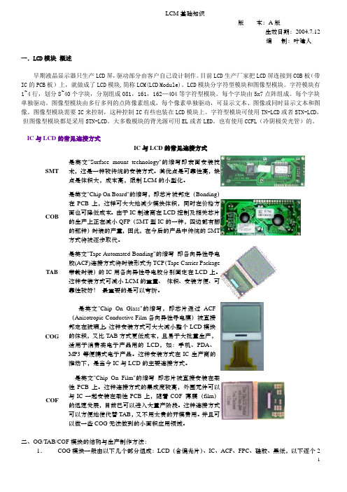
IC与LCD的常见连接方式IC与LCD的常见连接方式SMT 是英文"Surface mount technology"的缩写即表面安装技术,这是一种较传统的安装方式。
其优点是可靠性高,缺点是体积大,成本高,限制LCM的小型化。
COB 是英文"Chip On Board"的缩写,即芯片被邦定(Bonding)在PCB上,这样可大大地减少模块体积,同时在价格方面也可降低成本。
由于IC制造商在LCD控制及相关芯片的生产上正在减小QFP(SMT型IC的一种,四边都有脚的那种)封装的产量,因此,在今后的产品中传统的SMT 方式将被逐步取代。
TAB 是英文"Tape Automated Bonding"的缩写即各向异性导电胶(ACF)连接方式将封装形式为TCP(Tape Carrier Package 带载封装)的IC用各向异性导电胶分别固定在LCD上。
这种安装方式可减小LCM的重量、体积、安装方便、可靠性较好!最重要的是可以弯折。

60 GHz radar form factor module based on Infineon reference designUser manual and integration instructions for host product manufacturersAbout this documentScope and purposeThis document is the user manual with integration instructions for the radar embedded form factor (FF) module with presence detection software.Intended audienceManufacturers who intend to integrate the Infineon 60 GHz radar (BGT60TR13C) embedded form factor solution into their host product.Table of contentsAbout this document (1)Table of contents (2)1Introduction (4)1.1General features (4)1.2Presence detection features (4)2Hardware information (5)2.1Block diagram (5)2.2Module pin definitions (6)2.3Recommended operating conditions (7)2.4Module RF parameters (8)3UART interface connection (9)3.1Example command (9)4Radar radiation pattern (10)4.1Test setup (10)4.2Radiation pattern (10)5FCC considerations (12)5.1List of applicable FCC rules (12)5.2Specific operational use conditions (12)5.3Limited module procedures (12)5.4Trace antenna design (13)5.5RF exposure considerations (13)5.6Antennas (13)5.7Label and compliance information (13)5.8Information on test modes and additional testing requirements (13)5.9Test mode command (13)5.10Important notes (14)6Reference design (15)6.1Design recommendation (15)6.2Integration of module without RF shield into host product (15)7Module information (17)7.1Module dimensions (17)7.2Recommended land pattern (18)8SMT/baking information (19)8.1Baking recommendations (19)8.2SMT recommendations (19)9Revision history (21)Glossary Table 1Abbreviations1IntroductionMotion sensing is a standard feature present in many devices. Today’s devices become smarter by knowing if the user is around or not. Traditionally, motion sensors have been designed using passive infrared sensing (PIR). As simple as PIR is, there are performance limitations. For example, PIR sensors cannot detect micro motions. In addition, they require a lens, whereas radar sensors can be covered and disguised behind plastic enclosures. Infineon’s presence detection sensor module integrates 60 GHz mmWave technology. The module simplifies the implementation of mmWave sensors in the band of 61.0 to 61.5 GHz, and it includes the ARM® Cortex®-M4F based processor system, 1TX 3RX antennas and onboard regulator. This presence detection sensor module targets low-power and high-resolution presence detection in smart home, office, and diverse other use cases.1.1General features∙ARM® Cortex®-M4F 150 MHz, 1024 kB Flash, 288 kB RAM∙Built-in antennas (1TX 3RX)∙Built-in regulator∙UART interface and GPIOs∙ 3.6~5 V power input∙26-pin pitch 1.27 mm castellated holes∙Dimensions: 20 x 15 x 2.3 mmFigure 160 GHz radar form factor module1.2Presence detection features∙Low power and high resolution∙Presence sensing for home, office and commercial buildings∙Adjustable detection range∙Field of view of radar: azimuth: ±45 degrees/elevation: ±40 degrees∙Immune to environmental factors such as temperature, wind, sunlight and dust/debris∙Detection range:o Detection up to 10 m for macro motion (1)o Detection up to 5 m for micro motion (2)(1) Macro motion: Human movements.(2) Micro motion: Stationary human (normally breathing and blinking eyes) in sitting or standing position with no active movements for at least 30 s.2Hardware information2.1Block diagramFigure 2Module block diagramThe main components of the module are the 60 GHz radar chip, the ARM® based MCU and the 80 MHz oscillator. The module has its own power supply regulation. UART is the communication interface to the host device.2.2Module pin definitions Figure 3Components on the moduleTable 3P2 Pin definitions2.3Recommended operating conditions(1)Based on firmware 237a4fe version.(2)Means ambient temperature when working.2.4Module RF parameters1Fixed by firmware to comply with granted FCC certification. Figure 4Module – E- and H-planeUART interface connection3UART interface connectionA UART interface is used to communicate with the radar module through binary commands. The UART TX and RX pins operate at TTL 3.3 V level. A detailed configuration of the UART interface is shown in the table below.3.1Example commandExample command to get firmware version:Command send to UART_RXD9 00 00 00 B4 DFReply command receive at UART_TXD9 00 1E 00 50 72 65 73 65 6E 63 65 44 65 74 65 63 74 5F 31 2E 33 2E 30 20 28 31 35 36 61 34 62 63 29 52 EFThe binary command is in the format of header + length + payload + checksum. For detailed information please refer to the “Infineon BGT60TR13C embed MCU4 binary command protocol manual”.Radar radiation pattern4Radar radiation pattern 4.1Test setupE-planeFigure 54.2Radiation patternFigure 6Radiation pattern of the E-planeRadar radiation patternFigure 7Radiation pattern of the H-plane5FCC considerationsThe reference module has been certified at FCC according to the rules as stated in chapter 5.1.Host product manufacturers must immediately file a 2.933 Change-in-ID application to obtain their own FCC ID for the module, and then a C2P application to authorize the module in their specific host device(s).Host product manufacturers are advised to carefully read the whole of chapter 5 and follow the guidelines according to KDB 996369 D04, or the latest updates of it.5.1List of applicable FCC rulesThe modular transmitter was tested according to the following rules:∙FCC Rules and Regulations Part 15, Subpart A – General (September 2019)∙Part 15, Subpart A, Section 15.31 Measurement standards∙FCC Rules and Regulations Part 15, Subpart C – Intentional Radiators (September 2019)∙Part 15, Subpart C, Section 15.203 Antenna requirements∙Part 15, Subpart C, Section 15.204 External radio frequency power amplifiers and antenna modifications∙Part 15, Subpart C, Section 15.205 Restricted bands of operation∙Part 15, Subpart C, Section 15.207 Conducted limits∙Part 15, Subpart C, Section 15.209 Radiated emission limits, general requirements∙Part 15, Subpart C, Section 15.255 Operation within the band 57 to 71 GHz.The modular transmitter is only FCC authorized for the specific rule parts listed on the grant. The host product manufacturer is responsible for compliance with any other FCC rules that apply to the host not covered by the modular transmitter grant of certification.5.2Specific operational use conditions∙The module is classified for use in fixed equipment, refer to chapter 5.5.∙The module is FCC- certified for the operating frequency range 61 to 61.5 GHz.∙The application software (SW) has the firmware (FW) ID 1.0.0.5.3Limited module proceduresThe modular transmitter is approved by FCC as a “limited module” due to the following limitations: ∙The module does not have its own RF shielding.∙The module does not have an FCC ID label attached to it. FCC ID: 2AYSQ-6011Notes:∙See also chapter 5.5 for human exposure considerations.∙The module has not been tested for simultaneous transmission operations.∙Refer to chapter 6.2 for integration methods that address the limitation due to RF shielding.5.4Trace antenna designNot applicable.5.5RF exposure considerations∙The performed human exposure evaluation is described in the “Human exposure RF test report” No. : T46134-04-00HS∙The module is classified for use in fixed equipment.o The host product operating conditions must be such that there is a minimum separation distance of 20 cm (or possibly greater than 20 cm) between the module and nearby persons.o The host product manufacturer is required to provide the following text in its end user manual: “In order to comply with FCC RF Exposure requirements this device must be operated with aminimum separation distance of 20 cm between the equipment and a person’s body.”5.6AntennasThe antenna is integrated into the radar chip (on-chip antenna).Type: Linear polarized strip patch array antenna; gain 5 dBi.5.7Label and compliance informationThe module does not have a FCC label attached to it. The host product manufacturer is advised to provide a physical or e-label stating “Contains FCC ID: ….” with the finished product. The manufacturer is advised to read “Guidelines for Labeling and User Information for RF Devices – KDB Publication 784748.”5.8Information on test modes and additional testing requirementsInfineon provides software that enables the host module manufacturer to operate the module in certain test modes, including the modes that have been used for FCC certification of the module:∙CW low frequency: Operates the module in CW at 61.019 GHz.∙CW mid frequency: Operates the module in CW at 61.249 GHz.∙CW high frequency: Operates the module in CW at 61.479 GHz.∙FMCW: Chirp mode V 1.0.0 (presence detection SW) according to FW version 1.0.0.The SW also provides additional options that might be useful in testing the host system – e.g. a mode that puts the module into sleep mode. See the next chapter for information on initializing and using the SW.5.9Test mode commandThe UART interface can be used to set up the module in test mode. The following table show the commands for entering different test modes. After power-up or reset, the module will be in presence detection mode, which is sending FMCW chirps. An acknowledge command will be sent from the module after a valid command is received.To enable RFCW mode, please follow the below command sequence:Disable presence detection →Enable RFCW output (low/mid/high)To resume chirp mode from RFCW mode, please follow the below command sequence:Disable RFCW output →Enable presence detection5.10Important notesThe host product manufacturer must provide the below text to the end-user:a) Changes or modifications not expressly approved by the party responsible for compliance could void the user’s authority to operate the equipment.b) This device complies with Part 15 of the FCC rules. Operation is subject to the following conditions:∙This device may not cause interference.∙This device must accept any interference, including interference that may cause undesired operation of the device.6Reference design6.1Design recommendation∙Please reserve the test points of the UART for FW upgrade in the future.∙Please keep the module solder layer free of ground plane/trace rout in the “keep-out area” (shown in Figure 12).∙The power trace for DC_IN must be at least 20 mm wide.Figure 8Recommended layout of radar module6.2Integration of radar module into host productConsiderations when integrating are to ensure that the emissions from the host electronics are not advertently impacting the module and preventing proper operation. Conversely, the module emissions shall not prevent the rest of the host from operating properly. The complete host must still comply with applicable FCC regulations.Therefore, a verification of the final product must be done, by at least spot-checking emissions from the device while operating the host as a complete system. This testing should be performed with the host product configured in typical operational modes to check the fundamental frequency and spurious emissions for compliance with all applicable rules.To reduce the impact of the module on emissions, the host product manufacturer is advised to follow these guidelines:∙Ensure that the maximum amount of the radar signal is indeed leaving the host device by ensuring that the signal is not unnecessarily reflected inside the host. See the Infineon “60 GHz radar radome design guide” for proper distances to housing surfaces and recommended housing materials.∙Place the radar module inside the host as far away as technically feasible from other electronics that have been identified as susceptible to RF emissions, or identified to be a potential source of suchemissions. Such potential sources include other intentional transmitters or digital electronics operating at MHz clock rates.Put the PCB with the radar module soldered onto it within a separate section of the host, where it can be shielded from other host electronics. The shielding should be made of sheet metal, metal mesh or a metallic ink-coated material expressly designed as an effective shield. Any holes in the shield must be significantly smaller than the wavelength of the radiation that is being blocked. For 60 GHz radar that would mean maximum 0.5 mm.Whereas the first item should always be followed by the host manufacturer, the manufacturer can evaluate whether items two or three are suitable for the product and take measures to keep overall emissions below regulatory limits.7Module information7.1Module dimensionsTop view Side viewBottom viewFigure 9Module dimensions7.2Recommended land pattern Figure 10Recommended land pattern dimensions8SMT/baking information8.1Baking recommendationsBaking conditions:∙Follow MSL Level 4 to carry out the baking process.∙After the bag is opened, devices that will be subjected to reflow solder or other high-temperature processes must be:o mounted within 72 hours of factory conditions at less than 30°C/60 percent RHo stored at less than 10 percent RH.∙Devices require baking before mounting if the humidity indicator card reads more than 10 percent.∙If baking is required, devices may be baked for 8 hours at 125°C.8.2SMT recommendationsRecommended reflow profile:Figure 11Reflow profile of moduleNote: Add nitrogen during the reflow process to improve SMT solderability.∙Stencil thickness: 0.1~0.13 mm (recommended)∙Soldering paste (without Pb): SENJU N705-GRN3360-K2-V for best soldering effects.60 GHz Radar FF Module for Presence Detection based on InfineonReference DesignTable of contents9Revision history21Trademarks All referenced product or service names and trademarks are the property of their respective owners.Edition June 2021AppNote NumberPublished by Infineon Technologies AG 81726 Munich, Germany© 2021 Infineon Technologies AG. All Rights Reserved. Do you have a question about this document? Email: ******************** Document reference IMPORTANT NOTICE The information contained in this application note is given as a hint for the implementation of the product only and shall in no event be regarded as a description or warranty of a certain functionality, condition or quality of the product. Before implementation of the product, the recipient of this application note must verify any function and other technical information given herein in the real application. Infineon Technologies hereby disclaims any and all warranties and liabilities of any kind (including without limitation warranties of non-infringement of intellectual property rights of any third party) with respect to any and all information given in this application note. The data contained in this document is exclusively intended for technically trained staff. It is the responsibility of customer’s technical departments to evaluate the suitability of the product for the intended application and the completeness of the product information given in this document with respect to such application. For further information on the product, technology, delivery terms and conditions and prices please contact your nearest Infineon Technologies office ( ). WARNINGS Due to technical requirements products may contain dangerous substances. For information on the types in question please contact your nearest Infineon Technologies office. Except as otherwise explicitly approved by Infineon Technologies in a written document signed by authorized representatives of Infineon Technologies, Infineon Technologies’ products may not be used in any applications where a failure of the product or any consequences of the use thereof can reasonably be expected to result in personal injury.。
LCD 检验标准版本V1.5页码第2页共9页1.目的本标准为统一公司与客户LCD 成品验收、出货时的品质标准,保证产品质量满足客户要求.2.范围2.1适用于本公司提供的LCD 成品或散件中含LCD 成品的场合。
3.检验使用设备电测架、游标卡尺、显微镜、目视放大镜、防静电腕、指套、标签、高低温实验箱、冰箱、稳压电源(DC),台灯等。
4.抽样计划和引用标准4.1.1根据GB/T 2828.1---2003/ISO2859-1:1999,正常检查一次抽样方案,一般检验水平II。
4.1.2GB/T 2828.1---2003/ISO2859-1:1999逐批检查计数抽样程序及抽样表。
4.1.3GB/T 1619.96扭曲向列型液晶显示器件测试方法。
4.1.4GB/T 12848.91超曲向列型液晶显示器件总规范。
4.1.5GB2421-89电工电子产品基本环境实验规程。
5.检验条件和检验依据5.1外观:通常在25±5℃,45±20%RH 的环境,有足够的光线下(200~300cd/cm2),检验员的眼睛与LCD 之间的距离为30cm-40cm,正常应以反光方式进行检查,同时检查负图及全透/半透产品时LCD 下面需有背光源或灯箱进行透光检查。
5.2外观检验方法:正视角90°、上下左右30°±5°每个视角方向3-5秒、检验距离30-40cm。
检验项目抽检数AQL 判定LCD LCM 外观II 一次抽样MA=0.65MI=1.0MA=0.4MI=1.5尺寸N=3C=0C=0功能II 一次抽样MA=0.65MI=1.0MA=0.4MI=1.5LCD 检验标准版本V1.5页码第3页共9页5.2视区定义(具体见图纸)VA 区:有效可视范围非VA 区:非有效可视范围5.3采用裸眼检查(利用放大镜辅助进行缺陷大小测量除外)。
5.3.1如外观缺陷位于显示区外而又不影响装配及功能,则可作接受。
ITEMCONTENTSUNITLCD Type TFT/Transmissive/Normally white / Size7.0Inch Viewing Direction12:00 (without image inversion) O’ Clock Gray Scale Inversion Direction 6:00O’ Clock Number of Dots 800 x (RGB) × 480 / Driver ICBT81x / Interface TypeSPI/QSPI/ Module Memory Size 1 MB (BT81x) + 64 Mb (external flash) / Color Depth16.7M/ Pixel Arrangement RGB Vertical Stripe/ Surface Treatment Anti-glare / Clear (for CTP) / Input Voltage3.3V7” EVE3 SERIES LCD TFTRiTFT-70 seriesRev.1.0 2018-10-22L C D T F T M o d u l e S p e c i f i c a t i o nNote 1: RoHS, REACH SVHC compliant Note 2: LCM weight tolerance: ± 5%.CONTENTS (2)1 MODULE CLASSIFICATION INFORMATION (3)2 ASSEMBLY GUIDE - INTEGRATION (4)2.1 UxTouch assembly (5)2.2 Mounting frame (6)3 MODULE DRAWING (4)4 ABSOLUTE MAXIMUM RATINGS (5)5 ELECTRICAL CHARACTERISTICS (5)6 BACKLIGHT CHARACTERISTICS (5)7 ELECTRO-OPTICAL CHARACTERISTICS (5)8 INTERFACE DESCRIPTION (7)9 BT8x CONTROLLER SPECIFICATIONS (8)9.1 Serial host interface (8)9.2 Block Diagram (8)9.3 Host interface SPI mode 0 (9)9.4 Backlight driver block diagram (9)10 LCD TIMING CHARACTERISTICS (9)10.1 Clock and data input time diagram (9)10.2 Parallel RGB timing table (10)11 TOUCH SCREEN PANEL SPECIFICATIONS (10)11.1 Electrical characteristics (10)11.1.1 For capacitive touch panel (10)11.1.2 For resistive touch panel (11)11.2 Mechanical characteristics (11)11.2.1 For capacitive touch panel (11)11.2.2 For resistive touch panel (12)12 INSPECTION (12)12.1 Inspection condition (12)12.2 Inspection standard (13)13 RELIABILITY TEST (16)14 LEGAL INFORMATION (17)C – Capacitive Touch Panel10. VERSION 00(00-99)2ASSEMBLY GUIDE - INTEGRATIONThree options of rear side adhesive tape are available: double side adhesive tape 0.2 mm with 3M 467MP glue, foam double side adhesive tape 0.5 mm with DST 3M 9495LE glue or without any tape. There are also two versions of glass color: black and white.Rear side adhesive tape options:Double side adhesive tape with DST 3M 9495LE glue(total thickness 0.2mm)Foam double side adhesive tapewith 3M 9495LE glue (totalthickness 0.5mm)Without tapeCover glass color options:BLACK WHITEProduct options:NAME OF THEPRODUCTPART NUMBER DESCRIPTIONRiTFT-70 RVT70AQBNWN00 BT816, no touch panelRiTFT-70-RES RVT70AQBNWR00 BT816, resistive touch panelRiTFT-70-CAP RVT70AQBNWC00 BT815, capacitive touch panelRiTFT-70-FR RVT70AQBFWN00 BT816, no touch panel, mounting frame RiTFT-70-RES-FR RVT70AQBFWR00 BT816, resistive touch panel, mounting frame RiTFT-70-CAP-FR RVT70AQBFWC00 BT815, capacitive touch panel, mounting frameRiTFT-70-CAP-UX RVT70UQBNWC00 BT815, uxTouch, black cover glass, 0.2mm DST RVT70UQBNWC01 BT815, uxTouch, black cover glass, 0.5 mm DST RVT70UQBNWC02 BT815, uxTouch, black cover glass, no DST RVT70UQBNWC03 BT815, uxTouch, white cover glass, 0.2mm DST RVT70UQBNWC04 BT815, uxTouch, white cover glass, 0.5 mm DST RVT70UQBNWC05 BT815, uxTouch, white cover glass, no DST2.1UxTouch assemblyUxTouch are LCD TFT displays with specially designed projected capacitive touch panels. UxTouch display can be mounted without any holed in the housing. Our standard UxTouch displays include double-sided adhesive tape (DST) to stick TFT easily to the housing. Basic series include 4.3”, 5.0” and 7.0” display sizes.UxTouch models with double-side adhesive tape (PN with endings 00, 01, 03, 04) can be mounted by connecting the glass to the housing. Riverdi recommends to use support brackets assembled to display’s back. An additional support will stiffen the whole structure and minimize the influence of external factors such as vibration. Figure 1 and Figure 2 below show examples of using support elements.Figure 1. Example of using support bracketsFigure 2. Example of using fixing sleeves2.2Mounting frameFor dimension s 3.5”, 4.3”, 5.0” and 7.0” the product with mounting frame version is available. Thanks to the four catches attached to the side, frame provides strong assembly to the surface by mounting element (like the screw, see Figure 3). The frames are specially designed to fit Riverdi products perfectly. The diameter of the mounting hole is 3.5mm.Figure 3. Mounting frameRiTFT-703MODULE DRAWING© 2014 Riverdi Page 4 of 26 RiTFT-70-FR© 2018 Riverdi Page 5 of 26 RiTFT-70-CAP© 2018 Riverdi Page 6 of 26 RiTFT-70-CAP-FR© 2018 Riverdi Page 7 of 26 RiTFT-70-RESRiTFT-70-RES-FRRiTFT-70-UX4ABSOLUTE MAXIMUM RATINGSPARAMETER SYMBOL MIN MAX UNITSupply Voltage for Logic VDD 0 4.0 V Supply Voltage for LED inverter BLVDD 0 7.0 VInput Voltage for Logic VIN 0 4.0 VLED forward current (each LED) IF - 25 mA Operating Temperature T OP-20 70 °C PARAMETER SYMBOL MIN TYP MAX UNIT NOTES Supply Voltage For Module VDD 3.0 3.3 3.6 VInput Voltage for LED Inverter BLVDD 2.8 5.0 5.5 VLED Backlight Current IDD backlight- 290 363 mA BLVDD=3.3V LED Backlight Current IDD backlight- 180 225 mA BLVDD=5V Input Voltage ' H ' level V IH0.8VDD - VDD VInput Voltage ' L ' level V IL0 - 0.2VDD VInput Current I In TBD mAInput Current for module with CTP I InC TBD mAITEM SYMBOL MIN TYP MAX UNIT Voltage for LED backlight V l9.0 9.6 10.2 V Current for LED backlight I l170 180 200 mA LED Life Time - 30000 50000 - HrsLNote 1. Contrast Ratio(CR) is defined mathematically as below, for more information see Figure .Contrast Ratio =Average Surface Luminance with all white pixels (P1,P2,P3,P4,P5) Average Surface Luminance with all black pixels (P1,P2,P3,P4,P5)Note 2. Surface luminance is the LCD surface from the surface with all pixels displaying white. For more information, see Figure .Lv = Average Surface Luminance with all white pixels (P1, P2, P3, P4, P5)Note 3.The uniformity in surface luminance δ WHITE is determined by measuring luminance at each test position 1 through 5, and then dividing the maximum luminance of 5 points luminance by minimum luminance of 5 points luminance. For more information, see Figure .δ WHITE =Minimum Surface Luminance with all white pixels (P1,P2,P3,P4,P5) Maximum Surface Luminance with all white pixels (P1,P2,P3,P4,P5)Note 4. Response time is the time required for the display to transition from white to black (Rise Time, Tr) and from black to white (Decay Time, Tf). For additional information see FIG 1. The test equipment is Autronic-Melchers’s ConoScope series.Note 5.CIE (x, y) chromaticity, the x, y value is determined by measuring luminance at each test position 1 through 5, and then make average value.Note 6. Viewing angle is the angle at which the contrast ratio is greater than 2. For TFT module the contrast ratio is greater than 10. The angles are determined for the horizontal or x axis and the vertical or y axis with respect to the z axis which is normal to the LCD surface. For more information see Figure .Note 7. For viewing angle and response time testing, the testing data is based on Autronic-Melchers’s ConoScope series. Instruments for Contrast Ratio, Surface Luminance, Luminance Uniformity, CIE the test data is based on TOPCON’s BM-5 photo detector.Note 8. For TFT module, Gray scale reverse occurs in the direction of panel viewing angle.Figure 4. The definition of response timeFigure 5. Measuring method for Contrast ratio, surface luminance, Luminance uniformity, CIE (x, y) chromaticityFigure 6.The definition of viewing angle8INTERFACE DESCRIPTION9BT8x CONTROLLER SPECIFICATIONSBT8x or EVE3 (Embedded Video Engine 3) simplifies the system architecture for advanced human machine interfaces (HMIs) by providing functionality for display, audio, and touch as well as an object oriented architecture approach that extends from display creation to the rendering of the graphics.9.1Serial host interfaceFigure 7.SPI interface connection Figure 8. QSPI interface connectionSPI Interface– the SPI slave interface operates up to 30MHz.Only SPI mode 0 is supported. The SPI interface is selected by default (MODE pin is internally pulled low by 47k resistor).QSPI Interface–the QSPI slave interface operates up to 30MHz. Only SPI mode 0 is supported. The QSPI can be configured as a SPI slave in SINGLE, DUAL or QUAD data bus modes.By default the SPI slave operates in the SINGLE channel mode with MOSI as input from the master and MISO as output to the master. DUAL and QUAD channel modes can be configured through the SPI slave itself. To change the channel modes, write to register REG_SPI_WIDTH.9.2Block DiagramFigure 9. BT8x Block diagram9.3Host interface SPI mode 0Figure 10. SPI timing diagramFor more information about BT8x controller please go to official BT8x website.https:///Products/ICs/BT81X.html9.4Backlight driver block diagramBacklight enable signal is internally connected to BT8x Backlight control pin. This pin is controlled by two BT8x’s registers. One of them specifies the PWM output frequency, second one specifies the duty cycle. Refer to BT8x datasheet for more information.Figure 11. Backlight driver block diagram10LCD TIMING CHARACTERISTICS10.1Clock and data input time diagramFigure 12. Horizontal input timing diagramBT8xFigure 13. Vertical input timing diagram10.2Parallel RGB timing tablePARAMETER SYMBOL MIN TYP MAX UNIT Horizontal Display Area Thd - 800 - DCLK DCLK Frequency Fclk - 30 50 MHzOne Horizontal Line Th 889 928 1143 DCLK HS pulse width Thpw 1 48 255 DCLK HS Blanking Thb - 88 - DCLK HS Front Porch Thfp 1 40 255 DCLK Vertical Display Area Tvd - 480 - THVS period time Tv 513 525 767 THVS pulse width Tvpw 3 3 255 THVS Blanking Tvb - 32 - THVS Front Porch Tvfp 1 13 255 TH11TOUCH SCREEN PANEL SPECIFICATIONS11.1Electrical characteristicsNote: Avoid operating with hard or sharp material such as a ball point pen or a mechanical pencil except a polyacetal pen (tip R0.8mm or less) or a finger11.1.2For resistive touch panelITEMVALUEUNIT REMARK Min. Typ. Max.Linearity -3.0 - 3.0 % Analog X and Ydirections11.2Mechanical characteristicsNote 1: Force test condition, Input DC 5V on X direction, Drop off Polyacetal Stylus (R0.8), until output voltage stabilize, then get the R8.0mm Silicon rubber and do finger Activation force test. Next step, 9 points.Note 2: Measurement surface area conditions, Scratch 100,000 times straight line on the film with a stylus change every 20,000 times with Force: 250gf, Speed: 60mm/sec by R0.8 polaceteal stylus. Note 3: Pitting test, Pit 1, 000, 000 times on the film with R0.8 silicon rubber with Force: 250gf and Speed: 2 times/sec.11.2.2For resistive touch panelNote 1: Force test condition, Input DC 5V on X direction, drop off Polyacetal Stylus (R0.8), until output voltage stabilize, then get the R8.0mm Silicon rubber and do finger Activation force test. Next step, 9 points.ITEMVALUEUNIT REMARK Min. Typ. Max.12INSPECTIONStandard acceptance/rejection criteria for TFT module.12.1Inspection conditionAmbient conditions:•Temperature: 25±°C•Humidity: (60±10) %RH•Illumination: Single fluorescent lamp non-directive (300 to 700 lux) Viewing distance:35±5cm between inspector bare eye and LC D.Viewing Angle:U/D: 45°/45°, L/R 45°/45°12.2Inspection standard Item Criterion Black spots, whitespots, light leakage,Foreign Particle(round Type)D=(x+y)2*Spots density: 10 mmSize < 5”Average Diameter Qualified QtyD < 0.2 mm Ignored0.2 mm < D < 0.3 mm 30.3 mm < D < 0.5 mm 20.5 mm < D 0Size >= 5”Average Diameter Qualified Qty D<0.2 mm Ignored0.2 mm < D < 0.3 mm 40.3 mm < D < 0.5 mm 20.5 mm < D 0Clear spotsSize >= 5”Average Diameter Qualified Qty D<0.2 mmIgnored 0.2 mm < D < 0.3 mm 4 0.3 mm < D < 0.5 mm 2 0.5 mm < D*Spots density: 10 mm Size < 5”Average Diameter Qualified Qty D < 0.2 mmIgnored 0.2 mm < D < 0.3 mm 3 0.3 mm < D < 0.5 mm 2 0.5 mm < D 0Polarizer bubblesSize < 5”Average Diameter Qualified Qty D < 0.2 mmIgnored 0.2 mm < D < 0.5 mm 3 0.5 mm < D < 1 mm 2 1 mm < D 0 Total Q’ty 3Size >= 5”Average Diameter Qualified Qty D<0.25 mmIgnored 0.25 mm < D < 0.5 mm 3 0.5 mm < D 0Electrical Dot DefectSize < 5”itemQualified Qty Black do defect 4 Bright dot defect 2 Total Dot 5Size >= 5”itemQualified Qty Black do defect 5 Bright dot defect 2 Total Dot 5Touch panel spotSize < 5”Average Diameter Qualified QtyD < 0.2 mm Ignored0.2 mm < D < 0.4 mm 50.4 mm < D < 0.5 mm 213RELIABILITY TESTNO. TEST ITEM TEST CONDITION REMARKS1 High Temperature Storage 80±2°C/240hours Note 22 Low Temperature Storage -30±2°C/240hours Note 1,2Note 1: Without water condensation.Note 2:The function test shall be conducted after 2 hours storage at the room temperature and humidity after removed from the test chamber.14LEGAL INFORMATIONRiverdi makes no warranty, either expressed or implied with respect to any product, and specifically disclaims all other warranties, including, without limitation, warranties for merchantability, non-infringement and fitness for any particular purpose. Information about device are the property of Riverdi and may be the subject of patents pending or granted. It is not allowed to copy or disclosed this document without prior written permission.Riverdi endeavors to ensure that the all contained information in this document are correct but does not accept liability for any error or omission. Riverdi products are in developing process and published information may be not up to date. Riverdi reserves the right to update and makes changes to Specifications or written material without prior notice at any time. It is important to check the current position with Riverdi.Images and graphics used in this document are only for illustrative the purpose. All images and graphics are possible to be displayed on the range products of Riverdi, however the quality may vary. Riverdi is no liable to the buyer or to any third part for any indirect, incidental, special, consequential, punitive or exemplary damages (including without limitation lost profits, lost savings, or loss of business opportunity) relating to any product, service provided or to be provided by Riverdi, or the use or inability to use the same, even if Riverdi has been advised of the possibility of such damages.Riverdi products are not fault tolerant nor designed, manufactured or intended for use or resale as on line control equipment in hazardous environments requiring fail – safe performance, such as in the operation of nuclear facilities, aircraft navigation or communication systems, air traffic control, direct life support machines or weapons systems in which the failure of the product could lead directly to death, personal injury or severe physical or environmental damage (‘High Risk Activities’). Riverdi and its suppliers specifically disclaim any expressed or implied warranty of fitness for High Risk Activities. Using Riverdi products and devices in 'High Risk Activities' and in any other application is entirely at the buyer’s risk, and the buyer agrees to defend, indemnify and hold harmless Riverdi from any and all damages, claims or expenses resulting from such use. No licenses are conveyed, implicitly or otherwise, under any Riverdi intellectual property rights.。
LCM16032B使用说明书目 录序号 内 容 标 题 页码1 概述 22 字符型模块的特点 23 外形及接口引脚功能 2~34 基本原理 45 技术参数 46 时序特性 5~67 指令功能及硬件接口 6~101.概述方便、带中文字库、显示清晰,广泛应用于各种人机交流面板。
LCM16032B 液晶显示模块是160×32 点阵的汉字图形型液晶显示模块,可显示汉字及 图形,内置8192 个中文汉字(16X16 点阵)、128 个字符(8X16 点阵)及 64X256点阵显示RAM (GDRAM )。
可与CPU 直接接口,提供两种界面来连接 微处理机:8-位并行及串行两种连接方式。
具有多种功能:光标显示、画 面移位、睡眠模式等。
1.1结构牢:带PCB、背光、铁框1.2 IC 采用矽创公司ST7920,功能强大,稳定性好1.3功耗低:10 - 100mW(不带背光10mW,带背光不大于100mW); 1.4显示内容:●160*32点阵单色图片;●内置8192 个中文汉字(16X16 点阵)、128 个字符(8X16 点阵)及64X256点阵显示RAM (GDRAM ).1.5指令功能强:可组合成各种输入、显示、移位方式以满足不同的要求;1.6接口简单方便:采用3线SPI 串行接口,可只需3位MPU 的端口。
也可选用8位并行接口。
1.7工作温度宽:-20℃ - 70℃;1.8可靠性高:寿命为50,000小时(25℃)。
3.外形尺寸及接口引脚功能图1.外形尺寸我司专注于液晶屏及液晶模块的研发、制造。
所生产LCM16032B型液晶模块由于使用2.LC M 16032B图像型点阵液晶模块的特性模块的接口引脚功能引脚 符 号 名 称 功 能1 VSS接地 0V2 VDD 电路电源 5V,或3.3V 可选3 V0 LCD V0电压输入 可以通过此脚对LCD 驱动电压进行调整4RS(CS*)寄存器选择信号(串行时为片选:CS)1. 并行接口时:1:数据寄存器 0:指令寄存器2. 串行接口时:片选信号,低电平有效5 R/W(SID*) 读写选择(串行时为串行数据:SID) 1.并行接口时:0: 写 1:读2.串行时为串行数据输入:SID 6E(SCLK*)读写使能信号(串行时为串行时钟:SCLK) 1. 并行接口时:读写使能信号 2. 串行时为串行时钟:SCLK 7~14 D0~D7数据DB0~DB7并行接口时:数据总线DB0~DB7 串行接口时:无效,空脚4位并行接口时,DB4~DB7作为数据总线,DB0~DB3不起作用15 PSB 并行/串行选择 1:选择并行,0:选择串行,也可在PCB 上与VDD(1)或VSS(0)连接达到选择并/串接口。
1.8inch LCD ModuleUSER MANUALOVERVIEWThis product is 1.8inch resistive screen module with resolution 128x160. It has internal controller and uses SPI interface for communication. It has already basic functions: setting the point size, the line thickness, drawing circle, rectangle, and displaying English characters.We provide Raspberry Pi, STM32 and Arduino routines for this product.FEATURESDisplay type: TFTInterface: SPIDriver: ST7735SColors: 256KResolution: 128 x 160 (Pixel)Product size: 56.5 x 34(mm)Display size: 35.4(W) x 28.03(H)(mm)Pixel size: 0.219(W) x 0.219(H)(MM)Operating temperature: -30°C ~ 85°CINTERFACE DESCRIPTIONMarking Description3V3 3.3V powerGND groundDIN SPI data inputCLK SPI clockCS chip selectDC data/commandRST resetBL back lightPROGRAM ANALYSIS1.Working principles:ST7735S is 132 x 162 pixels LCD panel, but the product is 128 x 160 pixels LCD display.In the display there are two processes: the horizontal direction scanning – from the 2nd pixel, the vertical direction scanning – from the 1st pixel. So, you can see that positions of pixels in RAM correspond to their actual positions while displaying.The LCD supports 12-bit, 16-bit and 18-bit per pixel input formats. They correspond to RGB444, RGB565 and RGB666 color formats. This routine uses the RGB565 color format, which is commonly used.LCD uses 4-wired SPI communication interface, which can save a lot of GPIO ports and provides fast data transfer to LCD as well.munication protocolNote: there is a difference from traditional SPI. Here we only need display, so sine wires come from slave to host are hidden. The detailed information please refer to datasheet at page 58RESX: Reset. Pull-down while powering on the module. Generally set as 1IM2: data communication mode pin, which define usage of SPICSX: chip selection control pin. If CS=0 – the chip is selectedD/CX: data/command control pin, if DC=0 – command is written, otherwise – data are writtenSDA: transmitted RGB dataSCL: SPI clockThe SPI communication protocol of the data transmission uses control bits: clock phase (CPHA) and clock polarity (CPOL):The value of CPOL determines the level when the serial synchronous clock is in idle state. CPOL=0, that its idle level is 0.The value of CPHA determines the timing of the data bits relative to the clock pulses. CPHA=0, data is sampled at the first clock pulse edge.The combination of these two parameters provides 4 modes of SPI data transmission. The commonly used is SPI0 mode, it is that GPOL=0 and CPHA=0.From the figure above, SCLK begins to transfer data at the first falling edge. 8 bits data are transferred at one clock period. Use SPI0 mode, High bits transfer first, and LOW bits following. DEMO CODERaspberry Pi, STM32 and Arduino programs are provided, wherein Raspberry Pi provides BCM2835, WiringPi and python programs. It implements common graphical functions as drawing dot, line, rectangle, circle, setting their sizes and line with; filling arias, and displaying English characters of 5 common fonts and other display’s functions.Following instructions are offered for you convenienceRASPBERRY1.Enable SPI function of the Raspberry Pisudo raspi-configSelect: Advanced Options -> SPI -> yesActivate SPI hardware driver.2.Installation of librariesFore detailed information about libraries installation, please refer to this page:https:///wiki/Libraries_Installation_for_RPiIt is description of WiringPi, bcm2835 and python libraries installation.ageBCM2835 and WiringPi program should be only copied into directory of Raspberry Pi ()by samba or directly copy to the SD card). The following code are compied directly to the user directory of Pi.3.1Usage of BCM2835Run ls command as you can see below:bin: contains “.o” files.We don’t need to change it generallyFonts: contains 5 commonly used fontsPic: contains pictures used for displaying. The resolution of pictures must be 128x128,otherwise they cannot be displayed properly. And the format of pictures must be BMP.Obj: contains object files, like main.c, LCD_Driver.c, DEV_Config.c, LCD_GUI.c and theirheader files.main.c: The mian function. What need to note is that even though there are LCD_ScanDir used to control the direction of scanning, you need not to change it. Because this module is designed for Raspberry Pi, and for compatibility, we don’t recommend you to change it.DEV_Config.c:Definations of Raspberry Pi’s pins and the communication mode.LCD_Driver.c: Drive code of LCD. Need not change generally.LCD_BMP.c: Reading and analyzing BMP files and display themMakefile: This file contains compilation rules. If there are some changes in code, please run make clean to clean all the dependency file and executable files. Then execute make to compile the whole project and generate new executable files.tftlcd_1in8: executable file, generated by command makeTo run the program, you just need to run this command on terminal: sudo ./tftlcd_1in83.2WiringPiInput ls command, now you can see following:T he folders is similar to BCM2835’s. The only differences are that:1.WiringPi oprates by read/write the device files of Linux OS. and the bcm2835 is libraryfunction of Raspberry Pi’s CPU, it operates registers directl y. Thus, if you have usedbcm2835 libraries firstly, the usage of WiringPi code will be failed. In this case, you just need to reboot the system and try again.2.Due to the first difference, they underlying configuration are different. In DEV_Config.c,use wiringpiPi and the corresponding wiringPiSPI to provide underlay interfaces.The program executed by command sudo ./tftlcd_1in8 as well3.3PythonInput ls command, you can see that:LCD_1in8.py: Driver code of LCDLCD_Config.py: configuration of hardware underlaying interface.Executing program: sudo python LCD_1in8.pyNote: Some of the OS don’t have image libraries. In this case, you can run: sudo apt-get install python-imaging to install the image library.Image is an image processing library of python, represents any image by an image object.Thus, we can create a blank image by new, its size must be same as the display size of LCD.Then draw picture by Draw library, finally, transfer the image to the LCD. Here usingImage.load() too read RGB888 data of pixel, and convert to RGB565. Scanning every pixel then we could get the whole image for displaying. Its most important code is as below:4.Auto-runInitialize autorun in Raspberry Pi by configuring code of /etc/rc.local file:sudo vim /etc/rc.localBefore exit0 add:sudo python /home/pi/python/demo.py &Important: to place the program /home/pi/python/demo.py at the same director, you can input command pwd to get the path. And & character is necessary at the end of command line, otherwise probable need to reinstall the system (impossible terminate the process by pressing ctrl+c, impossible to login with pi user permission).STM32This demo uses XNUCLEO-F103RB developing board and is based on HAT library.1.Hardware connection1.8inch LCD XNUCLEO-F103RBVCC 3V3GND GNDDIN PA7CLK PA5CS PB6DC PA8RST PA9BL PC72.Expected resultProgram the demo into the development Board. Firstly the screen is refreshed completely, then a solid line, dashed line, open circle, solid circle, rectangle, solid torque are drawn and English characters are shown.ARDUINOUNO PLUS Arduino development board is used here.1.Hardware connection1.8inch LCD Arduino3.3V 3V3GND GNDDIN D11CLK D13CS D10DC D7RST D8BL D92.Due to small global memory 2Kb of UNO PLUS, the display can’t work in graphical mode,but the calling method is the same. Just because there is no enough memory, this demo is not provided.COMPATIBLE CODE PORTINGOffered demo is the commonly used programs, which are able to be ported. They can be used with two screens and the difference is only in initialization of them and their sizes.The usage method is defined by macros. In LCD_Driver.h or in LCD.h:#define LCD_1IN44#define LCD_1in8.As the name of the macros, they are used for 1.44inch and 1.8inch LCD separately. To use for one LCD, just need to comment other one.For example://#define LCD_1IN44#define LCD_1IN8Here we use it for 1.8inch LCD, so we comment the 1.44 macro. After saving, Run make clean to remove dependency files, and then run make to generate new executable files.。