1N5221B_07中文资料
- 格式:pdf
- 大小:139.31 KB
- 文档页数:7
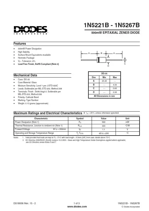
1N5221B to 1N5267BDocument Number 85588Rev. 1.7, 23-Mar-07Vishay Semiconductors194 9367Small Signal Zener DiodesFeatures•Silicon Planar Power Zener Diodes•Standard Zener voltage tolerance is ± 5 %•These diodes are also available in Mini-MELF case with the type designationTZM5221 ... TZM5267, SOT23 case with the type designations MMBZ5225 ... MMBZ5267 and SOD123 case with the types designations MMSZ5225 ... MMSZ5267 •Lead (Pb)-free component•Component in accordance to RoHS 2002/95/EC and WEEE 2002/96/ECApplications•Voltage stabilizationMechanical DataCase: DO35 Glass case Weight: approx. 125 mg Cathode Band Color: black Packaging codes/options:TAP/10 k per Ammopack (52 mm tape), 30 k/box TR/10 k per 13" reel, 30 k/boxAbsolute Maximum RatingsT amb = 25°C, unless otherwise specifiedThermal CharacteristicsT amb = 25°C, unless otherwise specifiedElectrical CharacteristicsT amb = 25°C, unless otherwise specifiedParameterTest conditionSymbol Value Unit Power dissipation T L ≤ 25°CP tot 500mW Z-currentI ZP tot /V ZmAParameterTest conditionSymbol Value Unit Thermal resistance junction to ambient air l = 4 mm, T L = constantR thJA 300K/W Junction temperature T j 175°C Storage temperature rangeT stg- 65 to + 175°CParameterT est conditionSymbol MinT yp.Max Unit Forward voltageI F = 200 mAV F1.1V 2Document Number 85588Rev. 1.7, 23-Mar-071N5221B to 1N5267B Vishay SemiconductorsElectrical Characteristics1N5221B...1N5267BPartnumber Nominal ZenerVoltage1)T est Current MaximumDynamicImpedance1)MaximumDynamicImpedanceTypicalTemperature ofCoeffizientMaximum Reverse LeakageCurrentat I ZT, V Z I ZT Z ZT at I ZT Z ZK at I ZK =0.25 mAat I ZT I R V R V mAΩΩα (%/K)µA V 1N5221B 2.420301200- 0.0851001 1N5222B 2.520301250- 0.0851001 1N5223B 2.720301300- 0.080751 1N5224B 2.820301400- 0.080751 1N5225B320291600- 0.075501 1N5226B 3.320281600- 0.070251 1N5227B 3.620241700- 0.065151 1N5228B 3.920231900- 0.060101 1N5229B 4.320222000+ 0.05551 1N5230B 4.720191900+ 0.03052 1N5231B 5.120171600+ 0.03052 1N5232B 5.620111600+ 0.03853 1N5233B62071600+ 0.0385 3.5 1N5234B 6.22071000+ 0.04554 1N5235B 6.8205750+ 0.05035 1N5236B7.5206500+ 0.05836 1N5237B8.2208500+ 0.0623 6.5 1N5238B8.7208600+ 0.0653 6.5 1N5239B9.12010600+ 0.06837 1N5240B102017600+ 0.07538 1N5241B112022600+ 0.07628.4 1N5242B122030600+ 0.07719.1 1N5243B139.513600+ 0.0790.59.9 1N5244B14915600+ 0.0820.110 1N5245B158.516600+ 0.0820.111 1N5246B167.817600+ 0.0830.112 1N5247B177.419600+ 0.0840.113 1N5248B18721600+ 0.0850.114 1N5249B19 6.623600+ 0.0860.114 1N5250B20 6.225600+ 0.0860.115 1N5251B22 5.629600+ 0.0870.117 1N5252B24 5.233600+ 0.0880.118 1N5253B25535600+ 0.0890.119 1N5254B27 4.641600+ 0.0900.121 1N5255B28 4.544600+ 0.0910.121 1N5256B30 4.249600+ 0.0910.123 1N5257B33 3.858700+ 0.0920.125 1N5258B36 3.470700+ 0.0930.127 1N5259B39 3.280800+ 0.0940.130 1N5260B43393900+ 0.0950.133 1N5261B47 2.71051000+ 0.0950.136 1N5262B51 2.51251100+ 0.0960.139 1N5263B56 2.21501300+ 0.0960.143 1N5264B60 2.11701400+ 0.0970.1461N5221B to 1N5267BDocument Number 85588Rev. 1.7, 23-Mar-07Vishay Semiconductors31)Based on dc-measurement at thermal equilibrium; lead length = 9.5 (3/8 "); thermal resistance of heat sink = 30 K/WTypical CharacteristicsT amb = 25°C, unless otherwise specified1N5265B 6221851400+ 0.0970.1471N5266B 68 1.82301600+ 0.0970.1521N5267B751.72701700+ 0.0980.156PartnumberNominal Zener Voltage1)Test CurrentMaximum Dynamic Impedance 1)Maximum DynamicImpedance T ypical T emperature of CoeffizientMaximum Reverse LeakageCurrentat I ZT , V ZI ZT Z ZT at I ZTZ ZK at I ZK = 0.25 mAat I ZT I R V R VmA ΩΩα (%/K)µA V Figure 1. Thermal Resistance vs. Lead LengthFigure 2. Typical Change of Working Voltage under OperatingConditions at T amb = 25 °C95 9611510150100200300400500R t h J A - T h e r m . R e s i s t . J u n c t i o n A m b i e n t (K /W )I - Lead Length (mm)1015201101001000V Z - V o l t a g e C h a n g e (m V )V Z - Z-V oltage (V )95 959805Figure 3. Typical Change of Working Voltage vs.Junction TemperatureFigure 4. Total Power Dissipation vs. Ambient Temperature0.V Z t n - R e l a t i v e V o l t a g e C h a n g eT j - J u nction Temperat u re (°C)95 95991201600100300400500600P t o t - T o t a l P o w e r D i s s i p a t i o n (m W )T am b - Am b ient Temperat u re (°C)20095 96022008040 4Document Number 85588Rev. 1.7, 23-Mar-071N5221B to 1N5267BVishay SemiconductorsFigure 5. Temperature Coefficient of Vz vs. Z-Voltage Figure 6. Diode Capacitance vs. Z-Voltage Figure 7. Forward Current vs. Forward Voltage 30- 551015V Z - Z-V oltage (V )5095 96004010200T K V Z - T e m p e r a t u r e C o e f f i c i e n t o f V Z (10-4/K )1015C D - D i o d e C a p a c i t a n c e (p F )V Z - Z-V oltage (V )95 96012050.010.11010095 9605I F - F o r w a r d C u r r e n t (m A )VF - For w ard V oltage (V )Figure 8. Z-Current vs. Z-VoltageFigure 9. Z-Current vs. Z-VoltageFigure 10. Differential Z-Resistance vs. Z-Voltage895 960420406080I Z - Z -C u r r e n t (m A )46V Z - Z-V oltage (V )152025300I Z -Z -C u r r e n t (m A )V Z - Z-V oltage (V )95 96071101001000(Ω)95 9606V Z - Z-V oltage (V )r Z - D i f f e r e n t i a l Z -R e s i s t a n c e1N5221B to 1N5267BDocument Number 85588Rev. 1.7, 23-Mar-07Vishay Semiconductors5Package Dimensions in millimeters (inches): DO35Figure 11. Thermal ResponseZ t h p - T h e r m a l R e s i s t a n c e f o r P u l s e C o n d . (K W )t P - P u lse Length (ms)95 960310-1100101102 6Document Number 85588Rev. 1.7, 23-Mar-071N5221B to 1N5267BVishay SemiconductorsOzone Depleting Substances Policy StatementIt is the policy of Vishay Semiconductor GmbH to1.Meet all present and future national and international statutory requirements.2.Regularly and continuously improve the performance of our products, processes, distribution and operatingsystems with respect to their impact on the health and safety of our employees and the public, as well as their impact on the environment.It is particular concern to control or eliminate releases of those substances into the atmosphere which are known as ozone depleting substances (ODSs).The Montreal Protocol (1987) and its London Amendments (1990) intend to severely restrict the use of ODSs and forbid their use within the next ten years. Various national and international initiatives are pressing for an earlier ban on these substances.Vishay Semiconductor GmbH has been able to use its policy of continuous improvements to eliminate the use of ODSs listed in the following documents.1.Annex A, B and list of transitional substances of the Montreal Protocol and the London Amendmentsrespectively2.Class I and II ozone depleting substances in the Clean Air Act Amendments of 1990 by the EnvironmentalProtection Agency (EPA) in the USA3.Council Decision 88/540/EEC and 91/690/EEC Annex A, B and C (transitional substances) respectively. Vishay Semiconductor GmbH can certify that our semiconductors are not manufactured with ozone depleting substances and do not contain such substances.We reserve the right to make changes to improve technical designand may do so without further notice.Parameters can vary in different applications. All operating parameters must be validated for each customer application by the customer. Should the buyer use Vishay Semiconductors products for any unintended or unauthorized application, the buyer shall indemnify Vishay Semiconductors against all claims, costs, damages, and expenses, arising out of, directly or indirectly, any claim of personal damage, injury or death associatedwith such unintended or unauthorized use.Vishay Semiconductor GmbH, P.O.B. 3535, D-74025 Heilbronn, GermanyDocument Number: 91000Revision: 18-Jul-081DisclaimerLegal Disclaimer NoticeVishayAll product specifications and data are subject to change without notice.Vishay Intertechnology, Inc., its affiliates, agents, and employees, and all persons acting on its or their behalf (collectively, “Vishay”), disclaim any and all liability for any errors, inaccuracies or incompleteness contained herein or in any other disclosure relating to any product.Vishay disclaims any and all liability arising out of the use or application of any product described herein or of any information provided herein to the maximum extent permitted by law. The product specifications do not expand or otherwise modify Vishay’s terms and conditions of purchase, including but not limited to the warranty expressed therein, which apply to these products.No license, express or implied, by estoppel or otherwise, to any intellectual property rights is granted by this document or by any conduct of Vishay.The products shown herein are not designed for use in medical, life-saving, or life-sustaining applications unless otherwise expressly indicated. Customers using or selling Vishay products not expressly indicated for use in such applications do so entirely at their own risk and agree to fully indemnify Vishay for any damages arising or resulting from such use or sale. Please contact authorized Vishay personnel to obtain written terms and conditions regarding products designed for such applications.Product names and markings noted herein may be trademarks of their respective owners.元器件交易网。