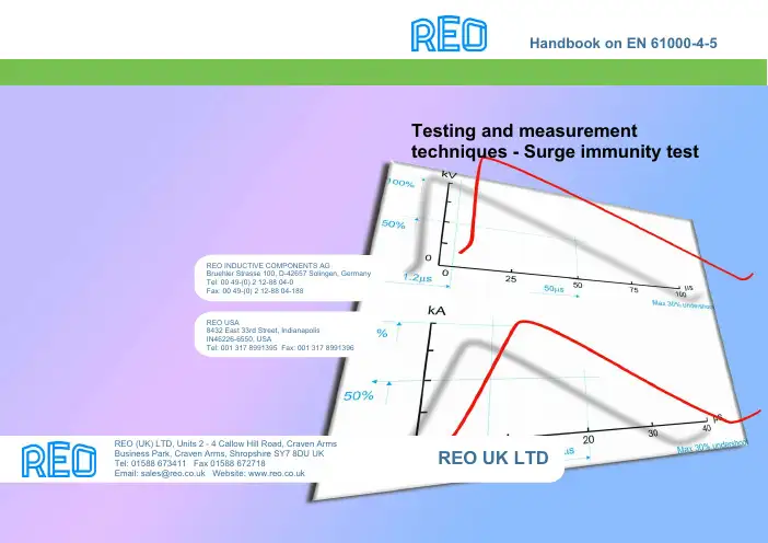
Eaton 197509Eaton Moeller® series EASY easyE4 control relay, basic unit (expandable, Ethernet), 100–240 VAC, 100–240 VDC (cULus: 100–110 VDC), digital inputs: 8, digital outputs: 4 relay, push-inSpécifications généralesEaton Moeller® series EASY Control relay197509401508194087558 mm 90 mm 72 mm 0.25 kg IEC/EN 61000-4-2 IEC 60068-2-27 IEC/EN 61000-4 EN 55011 EN 55022 IEC 60068-2-6 UL ListedUL Category Control No.: NRAQ, NRAQ7 IEC/EN 61131-2 IEC 60068-2-30 EN 61010 IEC/EN 61000-6-3 IEC/EN 61000-6-2 EN 50178UL File No.: E205091 DNV GL CEAccuracy of the real-time clock depending on ambient air temperature - fluctuations of up to ± 5 s/day (± 0.5 h ⁄year) are possibleEASY-E4-AC-12RCX1P Product NameCatalog Number EANProduct Length/Depth Product Height Product Width Product Weight Certifications Catalog NotesModel CodeExpandable Networkable (Ethernet)Relay outputTimerReal time clock IP2050/60 Hz (Digital inputs, at 115/230 V AC)50/60 Hz (Digital inputs, at 24 V DC)According to EN 50178, EN 61010-2-201, UL61010-2-201, CSA-C22.2 NO. 61010-2-20125,000 Operations (Fluorescent lamp load 1 x 58 W at 230/240 V AC, conventional, compensated)25,000 Operations (Fluorescent lamp load 10 x 58 W at 230/240 V AC, with upstream electrical device)25,000 Operations (Fluorescent lamp load 10 x 58 W at 230/240 V AC, uncompensated)25,000 Operations (Filament bulb load at 500 W, 115/120 V AC) 25,000 Operations (Filament bulb load at 1000 W, 230/240 V AC)1,000,000 OperationsTop-hat rail fixing (according to IEC/EN 60715, 35 mm)Screw fixing using fixing brackets ZB4-101-GF1 (accessories) Front build in possibleRail mounting possibleIII2Control relays easyE4MODBUSTCP/IP6 kV (contact-coil)5 % (transistor outputs)≤ 5 %Features Fitted with:Degree of protectionInput frequencyInsulation resistanceLifespan, electricalLifespan, mechanicalMounting methodOvervoltage categoryPollution degreeProduct categoryProtocolRated impulse withstand voltage (Uimp) Residual rippleEASYSOFT-SWLIC/easySoft70.5 Hz, Inductive load, Relay outputs 10 Hz, Relay outputs2 Hz, Resistive load/lamp load, Relay outputs easyE4 base device easyE4B 300 Light Pilot Duty, UL/CSA Control Circuit Rating Codes AC R 300 Light Pilot Duty, UL/CSA Control Circuit Rating Codes DC AC50 mm Drop height, Drop to IEC/EN 60068-2-310.3 mHorizontal Vertical15 g, Mechanical, according to IEC/EN 60068-2-27, Half-sinusoidal shock 11 ms, 18 Impacts According to IEC/EN 60068-2-6 10 - 57 Hz, 0.15 mm constant amplitude 57 - 150 Hz, 2 g constant acceleration795 - 1080 hPa (operation)-25 °C55 °C-40 °C70 °CClearance in air and creepage distances according to EN 50178, EN 61010-2-201, UL61010-2-201, CSA-C22.2 NO. 61010-2-201 Condensation: prevent with appropriate measures 5 - 95 % (IEC 60068-2-30, IEC 60068-2-78)ResolutionSoftwareSwitching frequencyTypeUsed with Utilization categoryVoltage type Drop and toppleHeight of fall (IEC/EN 60068-2-32) - max Mounting position Shock resistanceVibration resistanceAir pressureAmbient operating temperature - min Ambient operating temperature - max Ambient storage temperature - min Ambient storage temperature - max Environmental conditionsRelative humidityAir dischargeTerminal capacity1 min (Range H:M)1 s (Range M:S)5 ms (Range S)8 kV2 kV, Signal cable2 kV, Supply cableAccording to IEC/EN 61000-4-46 kV1 V/m at2 - 2.7 GHz (according to IEC EN 61000-4-3)10 V/m at 0.08 - 1.0 GHz (according to IEC EN 61000-4-3)3 V/m at 1.4 - 2 GHz (according to IEC EN 61000-4-3)10 V (according to IEC/EN 61000-4-6)Class B (EN 61000-6-3)1 kV, Supply cables, symmetrical, power pulses (Surge), EMC2 kV, Supply cables, asymmetrical, power pulses (Surge), EMC According to IEC/EN 61000-4-5 Level 410 ms 0.2 - 2.5 mm² (22 - 12 AWG), flexible with ferrule0.2 - 4 mm² (AWG 22 - 12), solid8 A4 W10 W200000 Operations at DC-13, 24 V DC, 1 A (500 Ops./h) 300000 Operations at AC-15, 250 V AC, 3 A (600 Ops./h)240 VMax. 300 V ACMax. 300 V DC85 - 264 V AC100/110/115/120/230/240 AC (-15 %/+10 %)50/60 Hz (± 5%)85 VAC264 VAC85 VDC264 VDC1 A DC, at R 300 (UL/CSA)10 A AC, at 240 V AC (UL/CSA)8 A DC, at 24 V DC (UL/CSA)5 A AC, max. thermal continuous current cos ϕ = 1 at B 300 (UL/CSA)Burst impulseContact dischargeElectromagnetic fieldsImmunity to line-conducted interference Radio interference classSurge ratingVoltage dips Conventional thermal current ith of auxiliary contacts (1-pole, open)Power consumptionPower lossRated breaking capacityRated insulation voltage (Ui)Rated operational voltageSupply frequencySupply voltage at AC, 50 Hz - minSupply voltage at AC, 50 Hz - maxSupply voltage at DC - minSupply voltage at DC - maxUninterrupted current≥ 1A (T), Fuse, Power supply Ethernet: RJ45 plug, 8-polePush in terminals10/100 MBit/sStatus indication of Power/RUNStatus indication of Ethernet: LED100 m (max. permissible per input I7 to I8), Digital inputs115/230 V AC40 m (max. permissible per input I1 to I6), Digital inputs 115/230 V ACCAT5± 2 s/day, Real-time clock to inputs (± 0.2 h⁄Year)± 1 %, Repetition accuracy of timing relays (of values)21 ms typ., Digital Inputs 100 - 240 V AC 60 Hz (I1 - I8), Delay time from 0 to 1, Debounce OFF21 ms typ., Digital Inputs 100 - 240 V AC 60 Hz (I1 - I8), Delay time from 1 to 0, Debounce OFF16⅔ ms, Digital inputs 115/230 V AC 60 Hz (I7, I8), Delay time from 1 to 0, Debounce OFF0.03 ms typ., Digital Inputs 100 - 240 V DC (I1 - I8), Delay time from 0 to 1, Debounce OFF0.03 ms typ., Digital Inputs 100 - 240 V DC (I1 - I8), Delay time from 1 to 0, Debounce OFF20 ms typ., Digital Inputs 100 - 240 V DC (I1 - I8), Delay time from 0 to 1, Debounce ON20 ms, Digital inputs 115/230 V AC 50 Hz (I7, I8), Delay time from 1 to 0, Debounce OFF20 ms typ., Digital Inputs 100 - 240 V DC (I1 - I8), Delay time from 1 to 0, Debounce ON2 x 6 mA (I7 - I8, at 230 V AC, 50 Hz, at signal 1)2 x 4 mA (I7 - I8, at 115 V AC, 60 Hz, at signal 1)6 x 0.25 mA (I1 - I8, at 115 V AC, 60 Hz, at signal 1)Condition 1: 79 - 264 V AC, Digital inputs, 115/230 V AC) Condition 0: 0 - 40 V AC, Digital inputs, 115/230 V AC)28/28 VA (DC, at R 300)3600/360 VA (AC, at B 300)Short-circuit protection Connection typeData transfer rateLED indicatorCable length Cable type AccuracyDelay timeInput currentInput voltageMaking/breaking capacity84VoltageRelay outputs in groups of 1> 500 mA (Relay outputs, Recommended for load: 12 V AC/DC) Current4 Relay OutputsNot permitted NoneBasic isolation: 600 V AC (Relay outputs)Between Analog inputs and Digital inputs: noBetween Relay outputs: yesBetween Digital inputs 115/230 V AC and Interface: yes Between Digital inputs 115/230 V AC and Memory card: noYesNone300 V AC, Between coil and contact, According to EN 50178 300 V AC, Between two contacts, According to EN 501784 W0 W0 W4 WMeets the product standard's requirements. Meets the product standard's requirements. Meets the product standard's requirements. Meets the product standard's requirements. Meets the product standard's requirements.eaton-electrical-timers-easy-control-relays-characteristic-curve-002.epsDA-DC-00004703.pdfDA-DC-00004708.pdfDA-CE-ETN.EASY-E4-AC-12RCX1PDA-MN-h1430deMN050009_FRMZ049014ENmz049001en.pdfVideo easy E4 control relayIL050020ZUDA-CD-uc_12rcx1DA-CS-uc_12rcx1Number of inputs (analog)Number of inputs (digital) Number of outputs (analog) Number of outputs (digital) OutputParallel switching Explosion safety category for gas Potential isolationProtection against polarity reversal Explosion safety category for dust Safe isolationEquipment heat dissipation, current-dependent PvidHeat dissipation capacity PdissHeat dissipation per pole, current-dependent PvidStatic heat dissipation, non-current-dependent Pvs10.2.2 Corrosion resistance10.2.3.1 Verification of thermal stability of enclosures10.2.3.2 Verification of resistance of insulating materials to normal heat10.2.3.3 Resist. of insul. mat. to abnormal heat/fire by internal elect. effects10.2.4 Resistance to ultra-violet (UV) radiation Characteristic curve Declarations of conformity eCAD modelGuide utilisateurInstallation videos Instructions d'installation mCAD modelDoes not apply, since the entire switchgear needs to be evaluated.Does not apply, since the entire switchgear needs to be evaluated.Meets the product standard's requirements.Meets the product standard's requirements.Meets the product standard's requirements.Does not apply, since the entire switchgear needs to be evaluated.Does not apply, since the entire switchgear needs to be evaluated.Is the panel builder's responsibility.Is the panel builder's responsibility.Is the panel builder's responsibility.Is the panel builder's responsibility.Is the panel builder's responsibility.The panel builder is responsible for the temperature rise calculation. Eaton will provide heat dissipation data for the devices.Is the panel builder's responsibility.Is the panel builder's responsibility.The device meets the requirements, provided the information in the instruction leaflet (IL) is observed.eaton-logic-relays-easy-control-relays-dimensions.eps 2723DIM-100eaton-modular-plc-easy-control-relays-3d-drawing-002.eps10.2.5 Lifting10.2.6 Mechanical impact10.2.7 Inscriptions10.3 Degree of protection of assemblies10.4 Clearances and creepage distances10.5 Protection against electric shock10.6 Incorporation of switching devices and components10.7 Internal electrical circuits and connections10.8 Connections for external conductors10.9.2 Power-frequency electric strength10.9.3 Impulse withstand voltage10.9.4 Testing of enclosures made of insulating material10.10 Temperature rise10.11 Short-circuit rating10.12 Electromagnetic compatibility10.13 Mechanical functionSchémasEaton Corporation plc Eaton House30 Pembroke Road Dublin 4, Ireland © 2023 Eaton. Tous droits réservés. Eaton is a registered trademark.All other trademarks areproperty of their respectiveowners./socialmedia。