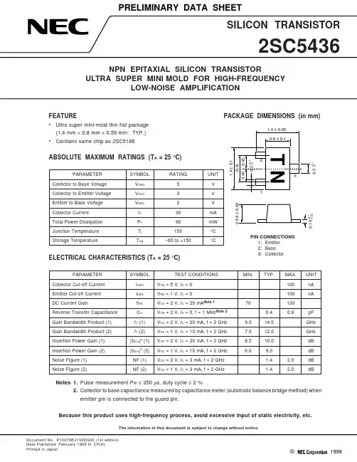
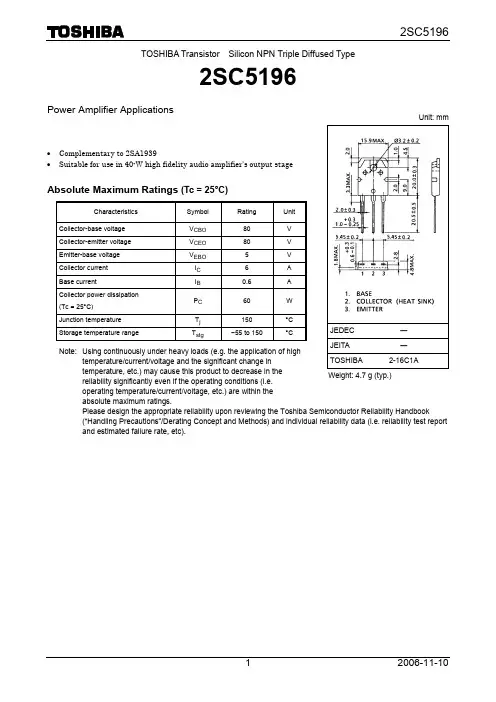
2SC5469资料
- 格式:pdf
- 大小:43.87 KB
- 文档页数:6
2SC5469
Silicon NPN Triple DiffusedCharacter Display Horizontal Deflection Output
ADE-208-631 (Z)1st. EditionOct. 1, 1998
Features
• High breakdown voltage
VCBO = 1500 V
• High speed switching
tf = 0.15 µsec(typ.) at fH=64kHz
Outline
TO–3PL
1. Base2. Collector3. Emitter123元器件交易网www.cecb2b.comDatasheet Title2Absolute Maximum Ratings (Ta = 25°C)
ItemSymbolRatingsUnit
Collector to base voltageVCBO1500V
Collector to emitter voltageVCEO700V
Emitter to base voltageVEBO6V
Collector currentIC15A
Collector peak currentic(peak)30A
Collector power dissipationPCNote1125W
Junction temperatureTj150°C
Storage temperatureTstg–55 to +150°C
Note:1.Value at Tc = 25°C
Electrical Characteristics (Ta = 25°C)
ItemSymbolMinTypMaxUnitTest Conditions
Collector to emitter breakdownvoltageV(BR)CEO700——VIC = 10mA, RBE = •
Emitter to base breakdownvoltageV(BR)EBO6——VIE = 10mA, IC = 0
Collector cutoff currentICES——500µAVCE = 1500V, RBE = 0
DC current transfer ratiohFE110—40VCE = 5 V, IC = 1A
DC current transfer ratiohFE23.5—6.5VCE = 5 V, IC = 8A
Collector to emitter saturationvoltageVCE(sat)——5VIC = 10A, IB = 3A
Base to emitter saturationvoltageVBE(sat)——1.5VIC = 10A, IB = 3A
Fall timetf—0.20.4µsICP = 7A, IB1= 2.8AfH
= 31.5kHz
Fall timetf—0.15—µsICP = 7A, IB1= 1.8AfH = 64kHz元器件交易网www.cecb2b.comDatasheet Title3 Main Characteristics
0.8 A200
150
100
50
050100150200100
10
05100.10.20.51252015
2102050100Collector Power Dissipation Pc (W)
Case Temperature Tc (°C)Collector Power Dissipationvs. Temperature
Collector to Emitter Voltage V (V)CECollector Current I (A)
CTypical Output Characteristics
DC Current Transfer Ratio hFE
Collector Current I (A)CDC Current Transfer Ratio vs.Collector CurrentCollector Current I (A)
Collector to Emitter Voltage V (V)CECArea of Safe Operaion
5
BI = 0Tc = 25 °C15
2102050
0.10.5
0.2
1010005000L = 180 µHI = –1 Aduty < 1 %Tc = 25°CB2
2.0 A1.8 A1.6 A1.4 A1.2 A1.0 A
0.6 A
0.4 A
0.2 A
10Tc = –25 °C25 °C75 °C
V = 5 VCE元器件交易网www.cecb2b.comDatasheet Title4
0.0510
25
1
0.10.20.5
0.10.5
0.212510
0.10.20.51251010
5
00.8
0.6
0.4
0.2
00.40.81.21.62.0Collector to Emitter Saturation Voltage
CE(sat)
V (V)
Collector Current I (A)CCollector to Emitter Saturation Voltagevs. Collector Current
Collector Current I (A)CBase to Emitter Saturation Voltage
V (V)
BE(sat)Base to Emitter Saturation Voltagevs. Collector Current
Base Current I (A)BCollector to Emitter Saturation Voltage
V (V)
CE(sat)Collector to Emitter Saturation Voltagevs. Base Current
Fall Time t (µs)
f
Base Current I (A)B1Fall Time vs. Base Current
Tc = 25°C7 A9 AI = 5 AC
2.40.20.512520100.10.20.51252010I / I = 3CB
Tc = –25 °C25 °C75 °CI / I = 3CB
Tc = –25°C
25 °C75 °C
2.8I = 7 Af = 64 kHzTc = 25°CCPH0.1元器件交易网www.cecb2b.comDatasheet Title5Package Dimensions (Unit: mm)
1.6+0.25–0.1
0.6+0.25–0.16.0 ± 0.2
20.0 ± 0.3
5.45 ± 0.55.45 ± 0.5123
1.0
3.87.43.02.21.41.60.5
20.0 ± 0.6
2.5 ± 0.326.0 ± 0.35.0 ± 0.2
2.8 ± 0.23.3 ± 0.2
Hitachi CodeEIAJJEDECTO–3PL——元器件交易网www.cecb2b.comDatasheet Title6Cautions1.Hitachi neither warrants nor grants licenses of any rights of Hitachi’s or any third party’s patent,
copyright, trademark, or other intellectual property rights for information contained in this document.
Hitachi bears no responsibility for problems that may arise with third party’s rights, includingintellectual property rights, in connection with use of the information contained in this document.
2.Products and product specifications may be subject to change without notice. Confirm that you have
received the latest product standards or specifications before final design, purchase or use.
3.Hitachi makes every attempt to ensure that its products are of high quality and reliability. However,
contact Hitachi’s sales office before using the product in an application that demands especially high
quality and reliability or where its failure or malfunction may directly threaten human life or cause risk
of bodily injury, such as aerospace, aeronautics, nuclear power, combustion control, transportation,
traffic, safety equipment or medical equipment for life support.
4.Design your application so that the product is used within the ranges guaranteed by Hitachi particularly
for maximum rating, operating supply voltage range, heat radiation characteristics, installation
conditions and other characteristics. Hitachi bears no responsibility for failure or damage when used
beyond the guaranteed ranges. Even within the guaranteed ranges, consider normally foreseeable
failure rates or failure modes in semiconductor devices and employ systemic measures such as fail-
safes, so that the equipment incorporating Hitachi product does not cause bodily injury, fire or other
consequential damage due to operation of the Hitachi product.