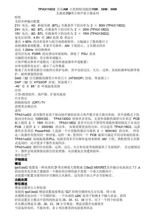
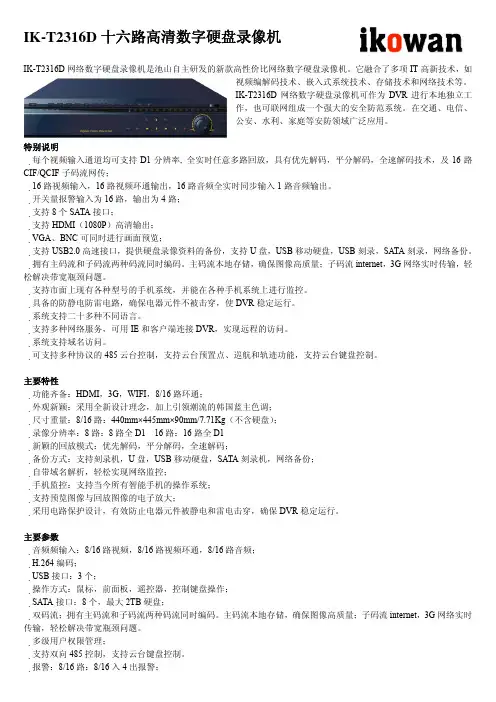
AS2316D资料
- 格式:pdf
- 大小:66.08 KB
- 文档页数:10
© ASTEC Semiconductor
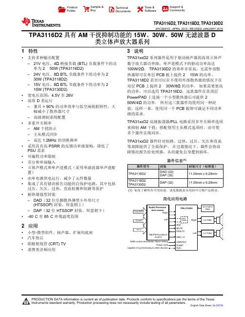
Description
The AS23xx is a housekeeping circuit for monitoring the outputs of powersupplies. It directly senses all the output rails without the need for external dividersand detects undervoltage and overvoltage. It also provides an additionalundervoltage comparator which may be configured with any arbitrary hysteresisto sense a divided down representation of the AC bulk voltage. The housekeepingsection provides all the features necessary to allow external caps to set thecommon timing features of PC type power supplies. In addition, negative rails maybe sensed without the necessity of a VEE connection, and negative sensing maybe disabled without affecting operation of the positive sense section. The 2.5 Vseries reference is available and can source up to 5 mA. This IC is available in16 lead packages. Outputs include a POK (Power OK) and a fault signal.
The AS2333 includes sensing for ±12 V, 5 V, and 3.3V. The AS2350 exchangesa -5 V sense capability for the 3.3 V input. The AS2316 monitors all supplyvoltages, but lacks CBD (Crow-Bar Driver). AS23xx
Secondary Side Housekeeping Circuit
Pin Configuration — Top viewFeatures
•Standard PC Power Good:UV Detection on 4 railsUV Detection of AC/Bulk supplyOV Detection on 4 railsOpen collector PG out
•Pogrammable Fault output:OVOV plus UVOV plus UV after startup delay
•OV Crow Bar Driver
•Digital ON/OFF input
•2.5V Voltage Reference
•Operates from 5V or 12V rail
Ordering Information
Package Temperature Range Order Code
16-Pin Plastic SOIC 0 to 105° C AS2316D
16-Pin Plastic SOIC 0 to 105° C AS2333D
16-Pin Plastic SOIC 0 to 105° C AS2350D
16-Pin Plastic DIP 0 to 105° C AS2316N
16-Pin Plastic DIP 0 to 105° C AS2333N
16-Pin Plastic DIP 0 to 105° C AS2350N
91AS2316 SOIC141VCCFAULT
132+12VVREF
123+5VUVB
114+3.3VDELAY
105-5VPOK
96-12VPGCAP
87GNDAC1615
HYSTOFF141VCCCBD
132+12VFAULT
123+5VVREF
114+3.3VUVB
105-12VDELAY
96GNDPOK
87HYSTPGCAP1615
OFFAC141VCCCBD
132+12VFAULT
123+5VVREF
114-5VUVB
105-12VDELAY
96GNDPOK
87HYSTPGCAP1615
OFFAC
141VCCFAULT
132+12VVREF
123+5VUVB
114+3.3VDELAY
105-5VPOK
96-12VPGCAP
87GNDAC1615
HYSTOFF141VCCCBD
132+12VFAULT
123+5VVREF
114+3.3VUVB
105-12VDELAY
96GNDPOK
87HYSTPGCAP1615
OFFAC141VCCCBD
132+12VFAULT
123+5VVREF
114-5VUVB
105-12VDELAY
96GNDPOK
87HYSTPGCAP1615
OFFACAS2316 PDIPAS2333 SOIC
AS2333 PDIPAS2350 SOIC
AS2350 PDIP元器件交易网www.cecb2b.comAS23xxSecondary Side Housekeeping Circuit
ASTEC Semiconductor92Functional Block Diagram
500UV
OV
UV
OV
UV
OV
UV1µAOVS
RQLatchSR
QLatcht20 µs delaySR
QLatch
nUVLatch
nUVLatchnUV
nUV
nUVnRESET
nRESETnOV
nOVnOVLatch
Disable
UV
Disable
1µA1µA
OV
chip bias2.5Vt20 µs delay
nAC WARNING
nOFF WARNINGnPOKnRESETnFAULT
nFAULTnOVHYST+12V
+5V
+3.3V
- 5V
- 12V
AC
HYST
OFFVREF
VCCVREFVREFVREF
VCCVCCGND
VREFVCCVREFVREFVCCVCCVCCVREFVCCVCCVCCFAULT
CBD Latch powers upin RESET state.
CBD
UVB
PGCAP
POK
DELAY
VREF元器件交易网www.cecb2b.comSecondary Side Housekeeping CircuitAS23xx
93ASTEC SemiconductorPin Function Description (For AS2333 / AS2350)
Pin NumberFunctionDescription
1VCCPower input to the chip.
2+12 VInput for overvoltage and undervoltage for the +12 V rail.
3+5 VInput for overvoltage and undervoltage for the +5 V rail.
4+3.3/–5 VInput for overvoltage and undervoltage for the +3.3V rail or –5 V rail, depending onproduct option.
5–12 VInput for overvoltage and undervoltage for the –12 V rail. This function maydisabled by tying this pin to a positive voltage above 2.4 V.
6GNDSignal ground and silicon substrate.
7HYSTOpen collector output of the AC undervoltage comparator. A resistor between this pinand AC will provide hysteresis to the AC undervoltage sensing.
8OFFPulling this pin low will reset the FAULT latch and discharge the start-up timingcapacitors, UVB and PG CAP, allowing normal start-up for the system. Pulling this pinhigh will send the FAULT signal high, prompting a system shutdown.
9ACNon-inverting input to the AC undervoltage sensing comparator. If the AC pin isless than 2.5 V, POK goes low and UVB cap discharges.
10PG CAPA cap to ground provides a delay between undervoltage sensing becoming goodand the POK output going high. Cap discharges whenever an output or ACundervoltage is detected.
11POKOpen collector output of the undervoltage sensing comparators. This pin goes lowupon an undervoltage condition. Except for the delay set by the PG CAP, this pinalways reflects the actual state of the undervoltage sensing.
12DELAYA cap to ground will delay the FAULT signal when the OFF pin is used to shut downthe system. The POK will signal a power fail warning immediately, but the FAULTshutdown of the power supply will be delayed.
13UVBA cap to ground provides start-up blanking of the undervoltage sensing portion of theFAULT signal. This pin may also be grounded to prevent undervoltage conditions fromtriggering the FAULT signal. This pin discharges the cap whenever AC goes low orFAULT pin goes high.