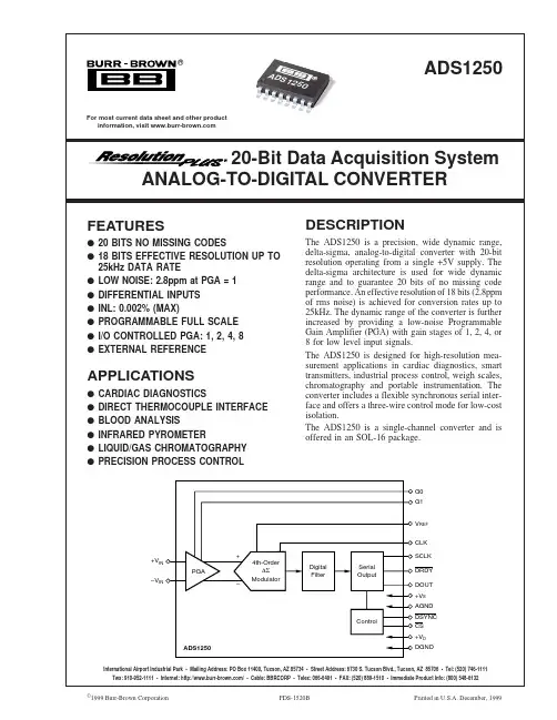
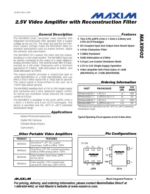
ADS-950MC中文资料
- 格式:pdf
- 大小:185.38 KB
- 文档页数:6
PRELIMINARY PRODUCT DATA18-Bit, 500kHz, Low-PowerSampling A/D ConvertersDATEL, Inc., Mansfield, MA 02048 (USA) · T el: (508) 339-3000, (800) 233-2765 Fax: (508) 339-6356 · Email: sales@ · Internet: ADS-9502+25°C 0 to +70°C–55 to +125°C ANALOG INPUT MIN.TYP .MAX. MIN.TYP.MAX. MIN.TYP .MAX.UNITS Input Voltage Range ➁—±5——±5——±5—Volts Input Resistance —500——500——500—W Input Capacitance —715—715—715pFDIGITAL INPUTLogic Levels Logic "1"+2.0——+2.0——+2.0——Volts Logic "0"——+0.8——+0.8——+0.8Volts Logic Loading "1"——+20——+20——+20µA Logic Loading "0"——–20——–20——–20µA Start Convert Positive Pulse Width ➂20500—20500—20500—nsSTATIC PERFORMANCE Resolution—18——18——18—Bits Integral Nonlinearity (f in = 10kHz)—±0.75——±1.5——±2—LSB Differential Nonlinearity (f in = 10kHz)–0.95±0.5+1–0.95±0.5+1–0.95±0.50+1.25LSB Full Scale Absolute Accuracy —±0.1±0.25—±0.25±0.4—±0.4±0.8%FSR Bipolar Zero Error (Tech Note 2)—±0.1±0.15—±0.15±0.25—±0.25±0.5%FSR Bipolar Offset Error (Tech Note 2)—±0.1±0.2—±0.2±0.3—±0.3±0.6%FSR Gain Error (Tech Note 2)—±0.1±0.25—±0.25±0.4—±0.4±0.9%No Missing Codes (f in = 10kHz)18——18——18——BitsDYNAMIC PERFORMANCE Peak Harmonics (–0.5dB)dc to 100kHz—–90——–90——–86—dB Total Harmonics Distortion (–0.5dB)dc to 100kHz—–89——–89——–85—dB Signal-to-Noise Ratio (w/o distortion, –0.5dB)dc to 100kHz9294—9294——92—dB Signal-to-Noise Ratio ➃(& distortion, –0.5dB)dc to 100kHz —86——86——82—dB Noise—3848—3848—38—µVrms Two-Tone Intermodulation Distortion (f in = 100kHz,240kHz, f s = 1MHz, –0.5dB)—–85——–85——–85—dB Input Bandwidth (–3dB)Small Signal (–20dB input)—TBD ——TBD ——TBD —MHz Large Signal (–0.5dB input)—TBD ——TBD ——TBD —MHz Feedthrough Rejection (f in = 500kHz)—84——84——84—dB Slew Rate—TBD ——TBD ——TBD —V/µs Aperture Delay Time —+20——+20——+20—ns Aperture Uncertainty —5——5——5—ps rms S/H Acquisition Time( to ±0.003%FSR, 10V step)—260——260——260—ns Overvoltage Recovery Time ➄—1——1——1—µs A/D Conversion Rate500——500——500——kHzPARAMETERSLIMITS UNITS +15V Supply (Pin 9)0 to +16Volts –15V Supply (Pin 8)0 to –16Volts +5V Supply (Pins 10, 14)0 to +6Volts –5V Supply (Pin 11)0 to –6Volts Digital Input (Pin 16)–0.3 to +V DD +0.3Volts Analog Input (Pin 4)±15Volts Lead Temperature (10 seconds)+300°CPARAMETERSMIN. TYP . MAX.UNITS Operating Temp. Range, Case ADS-951MC 0—+70°C ADS-951MM –55—+125°CThermal Impedance q jc —5—°C/Watt q ca—22—°C/Watt Storage Temperature Range –65—+150°C Package Type 32-pin,side-brazed, metal-sealed, ceramic TDIPWeight0.46 ounces (13 grams)ABSOLUTE MAXIMUM RATINGSPHYSICAL/ENVIRONMENTALFUNCTIONAL SPECIFICATIONS(T A = +25°C, ±V CC = ±15V, ±V DD = ±5V, 500kHz sampling rate, and a minimum 1 minute warmup ➀ unless otherwise specified.)3+25°C0 to +70°C –55 to +125°CANALOG OUTPUT MIN. TYP . MAX. MIN. TYP . MAX. MIN. TYP . MAX.UNITS Internal Reference Voltage +4.95+5.0+5.05+4.95+5.0+5.05+4.95+5.0+5.05Volts Drift—±30——±30——±30—ppm/°C External Current —1——1——1—mADIGITAL OUTPUTS Logic Levels Logic "1"+2.4——+2.4——+2.4——Volts Logic "0"——+0.4——+0.4——+0.4Volts Logic Loading "1"——–4——–4——–4mA Logic Loading "0"——+4——+4——+4mAOutput CodingComplementary Offset BinaryPOWER REQUIREMENTS Power Supply Ranges +15V Supply +14.5+15.0+15.5+14.5+15.0+15.5+14.5+15.0+15.5Volts –15V Supply –14.5–15.0–15.5–14.5–15.0–15.5–14.5–15.0–15.5Volts +5V Supply +4.75+5.0+5.25+4.75+5.0+5.25+4.75+5.0+5.25Volts –5V Supply–4.75–5.0–5.25–4.75–5.0–5.25–4.75–5.0–5.25Volts Power Supply Currents +15V Supply —+29——+29——+29—mA –15V Supply —–15——–15——–15—mA +5V Supply —+104——+104——+104—mA –5V Supply —–54——–54——–54—mA Power Dissipation— 1.45 1.65— 1.45 1.65— 1.45 1.65Watts Power Supply Rejection——±0.05——±0.05——±0.05%FSR/%VTHERMAL REQUIREMENTSAll DATEL sampling A/D converters are fully characterized and specified over operating temperature (case) ranges of 0 to +70°C and –55 to +125°C. All room-temperature (T A = +25°C)production testing is performed without the use of heat sinks or forced-air cooling. Thermal impedance figures for each device are listed in their respective specification tables.These devices do not normally require heat sinks, however,standard precautionary design and layout procedures should be used to ensure devices do not overheat. The ground and power planes beneath the package, as well as all pcb signal runs to and from the device, should be as heavy as possible to help conduct heat away from the package. Electrically-insulating,thermally-conductive "pads" may be installed underneath the package. Devices should be soldered to boards rather than "socketed", and of course, minimal air flow over the surface can greatly help reduce the package temperature.TECHNICAL NOTES1.Obtaining fully specified performance from the ADS-950requires careful attention to pc-card layout and powersupply decoupling. The device's analog and digital ground systems are not connected to each other internally. For optimal performance, tie all ground pins (3, 12 and 13)directly to a large analog ground plane beneath the package.Bypass all power supplies and the +5V REFERENCEOUTPUT (pin 5) to ground with 10µF tantalum capacitors in parallel with 0.1µF ceramic capacitors. Locate the bypass capacitors as close to the unit as possible. Tie a 47µF capacitor between COMPENSATION (pin 7) and ground.2.The ADS-950 achieves its specified accuracies without the need for external calibration. If required, the device's small initial errors can be reduced to zero using the adjustment circuitry shown in Figure 2. When using this circuitry, or any similar offset and gain calibration hardware, make adjust-ments following warmup. To avoid interaction, always adjust offset before gain. Float pin 6 if not using gain adjust circuits.Footnotes:➄This is the time required before the A/D output data is valid once the analog input is back within the specified range.6.02(SNR + Distortion) – 1.76 + 20 logFull Scale Amplitude Actual Input Amplitude➀All power supplies must be on before applying a start convert pulse. All supplies and the clock (START CONVERT) must be present during warmup periods. The device must be continuously converting during this time.➁Contact DATEL for other input voltage ranges.➂A 500kHz clock with a 1µsec positive pulse width (50% duty cycle) is used for all production testing. Any duty cycle may be used as long as a minimum positive pulse width of 20nsec is maintained. For applications requiring lower sampling rates, clock frequencies lower than 1MHz may be used.➃Effective bits is equal to:3.Applying a start convert pulse while a conversion is in progress (EOC = logic "1") will initiate a new and probably inaccurate conversion cycle. Data for the interrupted and subsequent conversions will be invalid.ADS-9504Zero/Offset Adjust Procedure1.Apply a train of pulses to the START CONVERT input(pin 16) so that the converter is continuously converting.2.For bipolar zero/offset adjust, apply –19µV to the ANALOGINPUT (pin 4).3.Adjust the offset potentiometer until the output code flickersequally between 01 1111 1111 1111 1111 and 10 00000000 0000 0000.Gain Adjust Procedure1.Apply –4.999943V to the ANALOG INPUT (pin 4).2.Adjust the gain potentiometer until all output bits are 1'sand the LSB flickers between 1 and 0.3.To confirm proper operation of the device, vary the appliedinput voltage to obtain the output coding listed in Table 2.BIPLOAR INPUT VOLTAGESCALE±5V MSB LSB+FS –1 LSB+4.999962000000 0000 0000 0000+3/4 FS+3.750000000111 1111 1111 1111+1/2 FS+2.500000001111 1111 1111 11110+0.000000011111 1111 1111 1111–1/2 FS–2.500000101111 1111 1111 1111–3/4 FS–3.750000110111 1111 1111 1111–FS +1 LSB–4.999962111111 1111 1111 1110–FS–5.000000111111 1111 1111 1111OUTPUT CODINGCOMPLEMENTARYOFFSET BINARYTable 2. Output CodingCALIBRATION PROCEDUREConnect the converter per Table 1 for the appropriate inputvoltage range. Any offset/gain calibration procedures shouldnot be implemented until the device is fully warmed up. Toavoid interaction, adjust offset before gain. The ranges ofadjustment for the circuits in Figure 2 are guaranteed tocompensate for the ADS-950's initial accuracy errors and maynot be able to compensate for additional system errors.A/D converters are calibrated by positioning their digital outputsexactly on the transition point between two adjacent digitaloutput codes. This is accomplished by connecting LED's to thedigital outputs and performing adjustments until certain LED's"flicker" equally between on and off. Other approaches employdigital comparators or microcontrollers to detect when theoutputs change from one code to the next.For the ADS-950, offset adjusting is normally accomplishedwhen the analog input is 0 minus ½LSB (–19µV). See Table 2for the proper bipolar output coding.Gain adjusting is accomplished when the analog input is atnominal full scale minus 1½LSB's (–4.999943V).INPUT VOLTAGE ZERO ADJUST GAIN ADJUSTRANGE(–½ LSB)(–FS +1½ LSB)±5V–19µV–4.999943Table 1. Input Connections5ADS-950DATEL makes no representation that the use of its products in the circuits described herein, or the use of other technical information contained herein, will not infringe upon existing or future patent rights. The descriptions contained herein do not imply the granting of licenses to make, use, or sell equipment constructed in accordance therewith. Specifications are subject to change without notice. The DATEL logo is a registered DATEL, Inc. trademark.DS-0????07/2000MECHANICAL DIMENSIONS INCHES (mm)ORDERING INFORMATIONOPERATING32-PIN MODEL NUMBER TEMP . RANGE PACKAGE ADS-950MC 0 to +70°C TDIP ADS-950MM–55 to +125°CTDIPACCESSORIES ADS-B950Evaluation Board (without ADS-950)Receptacles for PC board mounting can be ordered through AMP , Inc., Part # 3-331272-8(Component Lead Socket), 32 required. For availability of MIL-STD-883 product, contact DATEL.ISO 9001R E G I S T E R E DDATEL, Inc. 11 Cabot Boulevard, Mansfield, MA 02048-1151Tel: (508) 339-3000 (800) 233-2765 Fax: (508) 339-6356Email: sales@ Internet: DATEL (UK) LTD. Tadley, England Tel: (01256)-880444DATEL S.A.R.L. Montigny Le Bretonneux, France Tel: 01-34-60-01-01DATEL GmbH München, Germany Tel: 89-544334-0DATEL KK Tokyo, Japan Tel: 3-3779-1031, Osaka Tel: 6-6354-2025。