cd4081资料
- 格式:pdf
- 大小:98.72 KB
- 文档页数:7
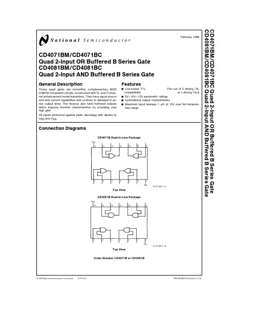
October 1987Revised January 1999CD4071BC • CD4081BC Quad 2-Input OR Buffered B Series Gate • Quad 2-Input AND Buffered B Series Gate © 1999 Fairchild Semiconductor Corporation DS005977.prf CD4071BC • CD4081BCQuad 2-Input OR Buffered B Series Gate •Quad 2-Input AND Buffered B Series GateGeneral DescriptionThe CD4071BC and CD4081BC quad gates are monolithiccomplementary MOS (CMOS) integrated circuits con-structed with N- and P-channel enhancement mode tran-sistors. They have equal source and sink currentcapabilities and conform to standard B series output drive.The devices also have buffered outputs which improvetransfer characteristics by providing very high gain.All inputs protected against static discharge with diodes toV DD and V SS.Featuress Low power TTL compatibility:Fan out of 2 driving 74L or 1 driving 74LSs5V–10V–15V parametric ratingss Symmetrical output characteristicss Maximum input leakage 1 µA at 15V over fulltemperature rangeOrdering Code:Devices are also available in Tape and Reel. Specify by appending the suffix letter “X” to the ordering code.Connection DiagramsPin Assignments for DIP and SOICCD4071BTop ViewCD4081BTop ViewOrder Number Package Number Package DescriptionCD4071BCM M14A14-Lead Small Outline Integrated Circuit (SOIC), JEDEC MS-120, 0.150” NarrowCD4071BCN N14A14-Lead Plastic Dual-In-Line Package (PDIP), JEDEC MS-001, 0.300” WideCD4081BCM M14A14-Lead Small Outline Integrated Circuit (SOIC), JEDEC MS-120, 0.150” NarrowCD4081BCN N14A14-Lead Plastic Dual-In-Line Package (PDIP), JEDEC MS-001, 0.300” Wide 2C D 4071B C • C D 4081B CSchematic DiagramsCD4071B1/4 of device shownJ = A + BLogical “1” = HIGH Logical “0” = LOW*All inputs protected by standard CMOS protection circuit.CD4081B1/4 of device shownJ = A • BLogical “1” = HIGH Logical “0” = LOWAll inputs protected by standard CMOS protection circuit.CD4071BC • CD4081BCAbsolute Maximum Ratings (Note 1)(Note 2)Recommended Operating ConditionsNote 1: “Absolute Maximum Ratings” are those values beyond which the safety of the device cannot be guaranteed. Except for “Operating Tempera-ture Range” they are not meant to imply that the devices should be oper-ated at these limits. The table of “Electrical Characteristics” provides conditions for actual device operation.Note 2: All voltages measured with respect to V SS unless otherwise speci-fied.DC Electrical Characteristics (Note 2)CD4071BC/CD4081BC Note 3: I OH and I OL are tested one output at a time.AC Electrical Characteristics (Note 4)CD4071BC T A = 25°C, Input t r ; t f = 20 ns, C L = 50 pF , R L = 200 k Ω, Typical temperature coefficient is 0.3%/°CNote 4: AC Parameters are guaranteed by DC correlated testing.Voltage at Any Pin −0.5V to V DD +0.5VPower Dissipation (P D )Dual-In-Line 700 mW Small Outline 500 mWV DD Range−0.5 V DC to +18 V DCStorage Temperature (T S )−65°C to +150°C Lead Temperature (T L )(Soldering, 10 seconds)260°C Operating Range (V DD )3 V DC to 15 V DC Operating T emperature Range (T A )CD4071BC, CD4081BC−40°C to +85°CSymbol ParameterConditions−40°C +25°C +85°C Units MinMax MinTyp Max MinMax I DDQuiescent Device V DD = 5V 10.00417.5µA CurrentV DD = 10V 20.005215µA V DD = 15V 40.006430µA V OLLOW Level V DD = 5V 0.0500.050.05V Output VoltageV DD = 10V |I O | < 1 µA0.0500.050.05V V DD = 15V 0.050.050.05V V OHHIGH Level V DD = 5V 4.954.955 4.95V Output VoltageV DD = 10V |I O | < 1 µA9.959.95109.95V V DD = 15V14.9514.951514.95V V ILLOW Level V DD = 5V , V O = 0.5V 1.52 1.5 1.5V Input VoltageV DD = 10V, V O = 1.0V 3.04 3.0 3.0V V DD = 15V, V O = 1.5V 4.064.0 4.0V V IHHIGH Level V DD = 5V , V O = 4.5V 3.5 3.53 3.5V Input VoltageV DD = 10V, V O = 9.0V 7.07.067.0V V DD = 15V, V O = 13.5V 11.011.0911.0V I OLLOW Level Output V DD = 5V , V O = 0.4V 0.520.440.880.36mA Current V DD = 10V, V O = 0.5V 1.3 1.1 2.250.9mA (Note 3)V DD = 15V, V O = 1.5V 3.6 3.08.8 2.4mA I OHHIGH Level Output V DD = 5V , V O = 4.6V −0.52−0.44−0.88−0.36mA Current V DD = 10V, V O = 9.5V −1.3−1.1−2.25−0.9mA (Note 3)V DD = 15V, V O = 13.5V −3.6−3.0−8.8−2.4mA I INInput CurrentV DD = 15V, V IN = 0V −0.30−10−5−0.30−1.0µA V DD = 15V, V IN = 15V0.3010−50.30 1.0µASymbol Parameter Conditions Typ Max Units t PHLPropagation Delay Time,V DD = 5V 100250ns HIGH-to-LOW LevelV DD = 10V40100ns V DD = 15V3070ns t PLHPropagation Delay Time,V DD = 5V 90250ns LOW-to-HIGH LevelV DD = 10V40100ns V DD = 15V3070ns t THL , t TLHTransition TimeV DD = 5V 90200ns V DD = 10V50100ns V DD = 15V4080ns C IN Average Input Capacitance Any Input 57.5pF C PDPower Dissipation CapacityAny Gate18pF 4C D 4071B C • C D 4081B CAC Electrical Characteristics(Note 5)CD4081BC T A = 25°C, Input t r ; t f = 20 ns, C L = 50 pF , R L = 200 k Ω, Typical temperature coefficient is 0.3%/°CNote 5: AC Parameters are guaranteed by DC correlated testing.Typical Performance CharacteristicsTypical Transfer CharacteristicsTypical Transfer Characteristics Typical Transfer CharacteristicsTypical Transfer CharacteristicsSymbol ParameterConditionsTyp Max Units t PHLPropagation Delay Time,V DD = 5V 100250ns HIGH-to-LOW LevelV DD = 10V 40100ns V DD = 15V 3070ns t PLHPropagation Delay Time,V DD = 5V 120250ns LOW-to-HIGH LevelV DD = 10V 50100ns V DD = 15V 3570ns t THL , t TLHTransition TimeV DD = 5V 90200ns V DD = 10V 50100ns V DD = 15V4080ns C IN Average Input Capacitance Any Input 57.5pF C PDPower Dissipation CapacityAny Gate18pF CD4071BC • CD4081BCTypical Performance Characteristics(Continued) 6C D 4071B C • C D 4081B CPhysical Dimensionsinches (millimeters) unless otherwise noted14-Lead Small Outline Integrated Circuit (SOIC), JEDEC MS-120, 0.150” NarrowPackage Number M14AF a irch ild d o e s n o t a ssu m e a n y re sp o n sib ility fo r u se o f a n y circu itry d e scrib e d, no circu it p a te n t licen se s a re im p lie d an d F a irch ild re se rv e s th e rig h t a t an y tim e w itho u t n o tice to ch a n g e sa id circu itry a n d sp e cificatio n s.CD4071BC • CD4081BC Quad 2-Input OR Buffered B Series Gate • Quad 2-Input AND Buffered B Series GateLIFE SUPPORT POLICYFAIRCHILD’S PRODUCTS ARE NOT AUTHORIZED FOR USE AS CRITICAL COMPONENTS IN LIFE SUPPORT DEVICES OR SYSTEMS WITHOUT THE EXPRESS WRITTEN APPROVAL OF THE PRESIDENT OF FAIRCHILD SEMICONDUCTOR CORPORATION. As used herein:1.Life support devices or systems are devices or systemswhich, (a) are intended for surgical implant into thebody, or (b) support or sustain life, and (c) whose failureto perform when properly used in accordance withinstructions for use provided in the labeling, can be rea-sonably expected to result in a significant injury to the user.2. A critical component in any component of a life support device or system whose failure to perform can be rea-sonably expected to cause the failure of the life support device or system, or to affect its safety or Physical Dimensions inches (millimeters) unless otherwise noted (Continued)14-Lead Plastic Dual-In-Line Package (PDIP), JEDEC MS-001, 0.300” WidePackage Number N14A。