Vishay新款3A同步降压稳压器简化设计并节省空间
- 格式:doc
- 大小:1.41 KB
- 文档页数:1
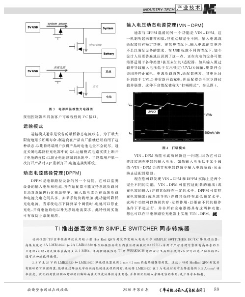
敬请登录网站在线投稿2018年第8期89图3电源路径线性充电器图按钮控制器和具备客户可编程性的I2C接口㊂运输模式运输模式通常是设备的最低静态电流状态㊂为了最大限度地延长贮藏寿命,制造商在产品出厂前就已经启用了这种状态,以期待终端用户获得产品时电池电量不会耗尽㊂通过关闭电源路径充电器中的Q2,运输模式电路实质上断开了电池的连接,以防止电池泄漏到系统中㊂当终端用户第一次打开产品时,Q2重新打开,电池连接到系统㊂动态电源路径管理(D P P M)D P P M是电源路径设备的另一个功能㊂它可以监测设备的输入电压和电流,并在适配器不能支持系统负载时自动对系统进行优先级排序㊂输入源电流会在系统负载和电池充电之间共享㊂如果系统负载增加,此功能可降低充电电流㊂当系统电压下降到某个阈值时,电池可以停止充电,并将电池放电以补充系统电流要求㊂此特性的实施可有效防止系统崩溃㊂输入电压动态电源管理(V I N D P M)通常与D P P M混淆的另一个功能是V I N D P M㊂这一机制听起来非常相似,但重点却完全不同㊂输入电源或适配器具有额定功率㊂在某些情况下,输入电源的功率并不足以满足设备的需求㊂在U S B标准不同的情况下,如今设计人员更普遍地认识到了这一点㊂正在充电的设备可能需要适用于各种类型(甚至未知的)适配器㊂如果输入源过载并导致输入电压低于欠压锁定(U V L O)阈值,则器件会关闭并停止充电㊂电源负载消失,适配器恢复㊂其电压回升到高于U V L O并重新开始充电,但适配器会再次立即过载并崩溃㊂这种不良情况被称为 打嗝模式 ㊂参见图4㊂图4打嗝模式V I N D P M功能可成功解决这一问题,因为它可以连续监测充电器的输入电压㊂如果输入电压低于某个阈值,V I N D P M会调节充电器以减少输入电流负载,从而防止适配器崩溃㊂现在您可以发现V I N D P M和D P P M实际上是两个完全不同的功能㊂V I N D P M可监控适配器的输出(或充电器的输入)并将其保持在一定的水平㊂D P P M可监控充电器输出(或系统导轨)并将其保持在最低预定水平㊂这两个功能可以协调共存,发挥作用,以便在不同的操作条件下平稳运行㊂并非所有充电器都具有这两种功能㊂您也可以在非电源路径充电器上实施V I N D P M㊂T I推出最高效率的S I M P L E S W I T C H E R同步转换器德州仪器(T I)宣布推出两款采用超小型H o t R o d Q F N封装的宽输入电压同步S I M P L E S W I T C H E R D C/D C降压稳压器㊂高集成度的3A L M R33630和2A L M R33620降压转换器具有业内最佳的满载效率(92%),专用于严苛并对可靠性有高要求的工业电源;同时,开关频率最高可至2.1MH z㊂这两款转换器与T I的W E B E N C H电源设计工具配合使用,不仅可以简化功率转化,还可以加速设计进程㊂3.8V至36V的L M R33630和L M R33620降压稳压器采用3m mˑ2m m的散热增强型封装㊂这款小巧的H o t R o d Q F N封装具有独特的可润湿侧翼,能够通过焊后光学检测简化制造流程的同时,还使得L M R33630在3A电流时具有业界最高的0.5A/m m2功率密度㊂优化的封装结构和对称的引脚布局最大限度地降低寄生电感,并帮助优化输入旁路电容的布局,减少传导和辐射㊂。

1Rev. 0DESCRIPTIONLT8618CHigh Efficiency 65V, 100mA Synchronous Buck RegulatorDemonstration circuit 3214A features the LT ®8618C , a high efficiency 65V, 100mA synchronous step-down reg-ulator in 12-Lead 2mm × 2mm LQFN package. The demo board is designed for 100mA at 5V output from a 5.9V to 65V input, with the switching frequency programmed at 2MHz.The LT8618C is a compact high efficiency, and high fre-quency synchronous monolithic step-down switching regulator , with internal soft-start capacitor , compensation network, BST and INTV CC capacitors.The operation mode can be configured via the SYNC/MODE pin for forced continuous mode, Burst Mode ® operation, or spread spectrum mode. The low quiescent current and high efficiency in Burst Mode make it an ideal solution for applications requiring highest efficiency atAll registered trademarks and trademarks are the property of their respective owners.PERFORMANCE SUMMARYlight load conditions, such as automotive housekeep-ing supplies, industrial sensors, flow meters, Internet of Things, and battery powered portable instruments.The demo board DC3214A has an EMI filter installed. The EMI performance of the board running in spread spec-trum mode is shown in Figure 2, where the red lines are CISPR25 Class 5 average limits. The circuit passes the average limit with a wide margin.The LT8618/LT8618C data sheet gives a complete description of the part, operation, and application infor-mation. The data sheet must be read in conjunction with this demo manual. Contact ADI applications engineer for technical support.Design files for this circuit board are available .Specifications are at T A = 25°CSYMBOL PARAMETER CONDITIONSMIN TYP MAX UNITSV IN Input Supply Range 5.965V V OUT Output Voltage4.8555.15V I OUT Maximum Output Current 100mA f SW Switching Frequency, FCM V IN = 12V , I OUT = 100mA 1.852 2.15MHz EFFEfficiency, FCMV IN = 12V , I OUT = 100mA89%2Rev. 0QUICK START PROCEDUREDC3214A is easy to set up to evaluate the performance of the LT8618C. Refer to Figure 1 for proper measurement equipment setup and follow the procedure below:1. With power off, connect the DC power supply to VEMI or VIN and GND, and load from VOUT to GND.2. By default, JP1 is connected to VOUT, and JP2 to FCM.3. Turn on the power at the input. Check for the proper output voltage (5V).4. Once the proper output voltage is established, adjust the line/load within the operating ranges and observe the output voltage regulation, ripple voltage, load transient, efficiency, and other parameters.Figure 1. Proper Measurement Equipment Setup3Rev. 0QUICK START PROCEDUREFigure 2. Conducted and Radiated EMI performance of the DC3214A. V IN = 14V, I OUT = 100mA, Spread Spectrum ModeCISPR25 Radiated EMI PerformanceCISPR25 Conducted Emission PerformanceVoltage MethodPARTS LISTITEM QTY REFERENCE PART DESCRIPTION MANUFACTURER/PART NUMBERRequired Circuit Components11C1CAP., 22µF, ALUM. ELECT., 63V, 20%, 6.3x7.7mm, CE-BS SUN ELECTRONIC INDUSTRIES CORP, 63CE22BS 23C2, C3, C10CAP., 1µF, X7S, 100V, 20%, 0805MURATA, GRJ21BC72A105ME11L31C8CAP., 0.01µF, X7R, 16V, 10%, 0603AVX, 0603YC103KAT2A41C9CAP., 4.7µF, X5R, 6.3V, 10%, 0603KEMET, C0603C475K9PACTU51C12CAP., 0.1µF, X7R, 100V, 10%, 0603AVX, 06031C104KAT2A61C15CAP., 22µF, X5R, 16V, 10%, 1206AVX, 1206YD226KAT2A71FB1IND., 300Ω, FERRITE BEAD, 25%, 250mA, 0402, AEC-Q200MMZ1005Y301CTD2581L1IND., 47µH, PWR, SHIELDED, 30%, 0.39A, 940mΩ, 3816WURTH ELEKTRONIK, 74403147092R1, R4RES., 1M, 1%, 1/10W, 0603, AEC-Q200VISHAY, CRCW06031M00FKEA101R2RES., 18.2k, 1%, 1/10W, 0603, AEC-Q200PANASONIC, ERJ3EKF1822111R3RES., 49.9k, 1%, 1/10W, 0603NIC, NRC06F4992TRF121R5RES., 187k, 1%, 1/10W, 0603, AEC-Q200PANASONIC, ERJ3EKF1873V131U1HIGH EFFICIENCY 60V/100mA, LQFN-12ANALOG DEVICES, LT8618CAV#TRMPBF Additional Demo Board Circuit Components10C5, C14CAP., 10pF, C0G, 16V, 5%, 0603, OPT20C6CAP., 10µF, X5R, 6.3V, 20%, 0603, OPT50R6, R7RES., OPTION, 0603Hardware: For Demo Board Only112E1-E12TEST POINT, TURRET, 0.094" MTG. HOLE, PCB 0.062" THK MILL-MAX, 2501-2-00-80-00-00-07-0 21JP1CONN., HDR, MALE, 1x3, 2mm, VERT, ST, THT, NO SUBS.WURTH ELEKTRONIK, 62000311121ALLOWED31JP2CONN., HDR, MALE, 2x4, 2mm, VERT, ST, THT WURTH ELEKTRONIK, 6200082112141XJP1, XJP2CONN., SHUNT, FEMALE, 2 POS, 2mm WURTH ELEKTRONIK, 6080021342154MP1-MP4STANDOFF, NYLON, SNAP-ON, 0.50"WURTH ELEKTRONIK, 7029350004Rev. 05Rev. 0Information furnished by Analog Devices is believed to be accurate and reliable. However , no responsibility is assumed by Analog Devices for its use, nor for any infringements of patents or other rights of third parties that may result from its use. Specifications subject to change without notice. No license is granted by implication or otherwise under any patent or patent rights of Analog Devices.SCHEMATIC DIAGRAMA N A L O G D E V I C E S H A S M A D E AB E S T E F F O R T T O D E S I G N AC I R C U I T T H A T M E E T S C U S T O M E R -S U P P L I ED S PE C IF I C A T I O N S ;H O W E V E R , I T R E M A I N S T H E C U S T O M E R 'S R E S P O N S I B I L I T Y T O6Rev. 0ANALOG DEVICES, INC. 202111/21ESD CautionESD (electrostatic discharge) sensitive device. Charged devices and circuit boards can discharge without detection. Although this product features patented or proprietary protection circuitry, damage may occur on devices subjected to high energy ESD. Therefore, proper ESD precautions should be taken to avoid performance degradation or loss of functionality.Legal Terms and ConditionsBy using the evaluation board discussed herein (together with any tools, components documentation or support materials, the “Evaluation Board”), you are agreeing to be bound by the terms and conditions set forth below (“Agreement”) unless you have purchased the Evaluation Board, in which case the Analog Devices Standard Terms and Conditions of Sale shall govern. Do not use the Evaluation Board until you have read and agreed to the Agreement. Your use of the Evaluation Board shall signify your acceptance of the Agreement. This Agreement is made by and between you (“Customer”) and Analog Devices, Inc. (“ADI”), with its principal place of business at One Technology Way, Norwood, MA 02062, USA. Subject to the terms and conditions of the Agreement, ADI hereby grants to Customer a free, limited, personal, temporary, non-exclusive, non-sublicensable, non-transferable license to use the Evaluation Board FOR EVALUATION PURPOSES ONL Y. Customer understands and agrees that the Evaluation Board is provided for the sole and exclusive purpose referenced above, and agrees not to use the Evaluation Board for any other purpose. Furthermore, the license granted is expressly made subject to the following additional limitations: Customer shall not (i) rent, lease, display, sell, transfer , assign, sublicense, or distribute the Evaluation Board; and (ii) permit any Third Party to access the Evaluation Board. As used herein, the term “Third Party” includes any entity other than ADI, Customer , their employees, affiliates and in-house consultants. The Evaluation Board is NOT sold to Customer; all rights not expressly granted herein, including ownership of the Evaluation Board, are reserved by ADI. CONFIDENTIALITY. This Agreement and the Evaluation Board shall all be considered the confidential and proprietary information of ADI. Customer may not disclose or transfer any portion of the Evaluation Board to any other party for any reason. Upon discontinuation of use of the Evaluation Board or termination of this Agreement, Customer agrees to promptly return the Evaluation Board to ADI. ADDITIONAL RESTRICTIONS. Customer may not disassemble, decompile or reverse engineer chips on the Evaluation Board. Customer shall inform ADI of any occurred damages or any modifications or alterations it makes to the Evaluation Board, including but not limited to soldering or any other activity that affects the material content of the Evaluation Board. Modifications to the Evaluation Board must comply with applicable law, including but not limited to the RoHS Directive. TERMINATION. ADI may terminate this Agreement at any time upon giving written notice to Customer . Customer agrees to return to ADI the Evaluation Board at that time. LIMITATION OF LIABILITY. THE EVALUATION BOARD PROVIDED HEREUNDER IS PROVIDED “AS IS” AND ADI MAKES NO WARRANTIES OR REPRESENTATIONS OF ANY KIND WITH RESPECT TO IT . ADI SPECIFICALL Y DISCLAIMS ANY REPRESENTATIONS, ENDORSEMENTS, GUARANTEES, OR WARRANTIES, EXPRESS OR IMPLIED, RELATED TO THE EVALUATION BOARD INCLUDING, BUT NOT LIMITED TO, THE IMPLIED WARRANTY OF MERCHANTABILITY, TITLE, FITNESS FOR A PARTICULAR PURPOSE OR NONINFRINGEMENT OF INTELLECTUAL PROPERTY RIGHTS. IN NO EVENT WILL ADI AND ITS LICENSORS BE LIABLE FOR ANY INCIDENTAL, SPECIAL, INDIRECT , OR CONSEQUENTIAL DAMAGES RESUL TING FROM CUSTOMER’S POSSESSION OR USE OF THE EVALUATION BOARD, INCLUDING BUT NOT LIMITED TO LOST PROFITS, DELAY COSTS, LABOR COSTS OR LOSS OF GOODWILL. ADI’S TOTAL LIABILITY FROM ANY AND ALL CAUSES SHALL BE LIMITED TO THE AMOUNT OF ONE HUNDRED US DOLLARS ($100.00). EXPORT . Customer agrees that it will not directly or indirectly export the Evaluation Board to another country, and that it will comply with all applicable United States federal laws and regulations relating to exports. GOVERNING LAW . This Agreement shall be governed by and construed in accordance with the substantive laws of the Commonwealth of Massachusetts (excluding conflict of law rules). Any legal action regarding this Agreement will be heard in the state or federal courts having jurisdiction in Suffolk County, Massachusetts, and Customer hereby submits to the personal jurisdiction and venue of such courts. The United Nations Convention on Contracts for the International Sale of Goods shall not apply to this Agreement and is expressly disclaimed.。


RT9193DS9193-09 March 2007300mA, Ultra-Low Noise, Ultra-Fast CMOS LDO RegulatorMarking Information For marking information, contact our sales representative directly or through a RichTek distributor located in your area, otherwise visit our website for detail.Ordering InformationGeneral DescriptionThe RT9193 is designed for portable RF and wireless applications with demanding performance and space requirements. The RT9193 performance is optimized for battery-powered systems to deliver ultra low noise and low quiescent current. A noise bypass pin is available for further reduction of output noise. Regulator ground current increases only slightly in dropout, further prolonging the battery life. The RT9193 also works with low-ESR ceramic capacitors, reducing the amount of board space necessary for power applications, critical in hand-he ld wireless devices. The RT9193 consumes less than 0.01μA in shutdown mode and has fast turn-on time less than 50μs.The other features include ultra low dropout voltage, high output accuracy, current limiting protection, and high ripple rejection ratio. Available in the 5-lead of SC-70, SOT-23and WDFN-6L 2x2 packages.Featuresz Ultra-Low-Noise for RF Applicationz Ultra-Fast Response in Line/Load Transient z Quick Start-Up (Typically 50μs)z < 0.01μA Standby Current When Shutdown z Low Dropout : 220mV @ 300mAz Wide Operating Voltage Ranges : 2.5V to 5.5V z TTL-Logic-Controlled Shutdown Input z Low Temperature Coefficient z Current Limiting Protection z Thermal Shutdown Protectionz Only 1μF Output Capacitor Required for Stability z High Power Supply Rejection Ratio z Custom Voltage AvailablezRoHS Compliant and 100% Lead (Pb)-FreeApplicationsz CDMA/GSM Cellular Handsets z Battery-Powered EquipmentzLaptop, Palmtops, Notebook Computers z Hand-Held Instruments z PCMCIA CardszPortable Information AppliancesNote :RichTek Pb-free and Green products are :`RoHS compliant and compatible with the current require- ments of IPC/JEDEC J-STD-020.`Suitable for use in SnPb or Pb-free soldering processes.`100% matte tin (Sn) plating.Pin Configurations (TOP VIEW)SC-70-5/SOT-23-5WDFN-6L 2x2VIN GNDBPVOUT EN23541ENGND BP NC VOUTVIN541236RT9193-Package Type U5 : SC-70-5B : SOT-23-5QW : WDFN-6L 2x2 (W-Type)Output Voltage 15 : 1.5V 16 : 1.6V : 49 : 4.9V50 : 5.0V1H : 1.85V 2H : 2.85V4G : 4.75VOperating Temperature Range P : Pb Free with Commercial StandardG : Green (Halogen Free with Commer- cial Standard)查询RT9193-49GQW供应商捷多邦,专业PCB打样工厂,24小时加急出货RT9193Function Block DiagramFunctional Pin DescriptionTypical Application CircuitBPENV V OUTRT9193DS9193-09 March 2007Electrical CharacteristicsAbsolute Maximum Ratings (Note 1)z Supply Input Voltage ------------------------------------------------------------------------------------------------------6V zPower Dissipation, P D @ T A = 25°CSC-70-5----------------------------------------------------------------------------------------------------------------------300mW SOT-23-5--------------------------------------------------------------------------------------------------------------------400mW WDFN-6L 2x2--------------------------------------------------------------------------------------------------------------606mW zPackage Thermal Resistance (Note 4)SOT-70-5, θJA ---------------------------------------------------------------------------------------------------------------333°C/W SOT-23-5, θJA ---------------------------------------------------------------------------------------------------------------250°C/W WDFN-6L 2x2, θJA ---------------------------------------------------------------------------------------------------------165°C/W z Junction T emperature -----------------------------------------------------------------------------------------------------150°C z Lead Temperature (Soldering, 10 sec.)-------------------------------------------------------------------------------260°Cz Storage T emperature Range --------------------------------------------------------------------------------------------−65°C to 150°C zESD Susceptibility (Note 2)HBM (Human Body Mode)----------------------------------------------------------------------------------------------2kV MM (Machine Mode)------------------------------------------------------------------------------------------------------200VRecommended Operating Conditions (Note 3)z Supply Input Voltage ------------------------------------------------------------------------------------------------------2.5V to 5.5V z EN Input Voltage -----------------------------------------------------------------------------------------------------------0V to 5.5Vz Junction T emperature Range --------------------------------------------------------------------------------------------−40°C to 125°C zAmbient T emperature Range --------------------------------------------------------------------------------------------−40°C to 85°C To be continuedRT9193Note 2. Devices are ESD sensitive. Handling precaution recommended.Note 3. The device is not guaranteed to function outside its operating conditions.Note 4.θJA is measured in the natural convection at T A = 25°C on a low effective thermal conductivity test board (Single Layer, 1S) of JEDEC 51-3 thermal measurement standard.Note 5. The dropout voltage is defined as V IN -V OUT, which is measured when V OUT is V OUT(NORMAL)− 100mV.RT9193DS9193-09 March 2007Dropout Voltage vs. Load Current05010015020025030000.050.10.150.20.250.3Load Current (A)D r o p o u t V o l t a g e (m V )Typical Operating CharacteristicsPSRR-80-60-40-20200.010.11101001000Frequency (kHz)PS R R (d B )10 100 1K 10K 100K 1M (Hz)EN Pin Shoutdown Threshold vs. Temperature0.50.7511.251.51.75-50-25255075100125Temperature E N P i n S h o u t d o w n T h r e s h o l d (V )(°C)Quiescent Current vs. Temperature6065707580859095-50-25255075100125Temperature Q u i e s c e n t C u r r e n t (u A )(°C)Output Voltage vs. Temperature1.21.31.41.51.61.71.8-50-25255075100125Temperature O u t p u t V o l t a g e (V )(°C)Time (500μs/Div)V IN = 5VC IN = C OUT = 1uFEN Pin Shutdown ResponseE N P i n V o l t a g e (V )O u t p u t V o l t a g e (V )RT9193-28CU5No Load10 5 02 1 0RT9193Time (10ms/Div)V IN = 4.5VC IN = C OUT = 1uF, X7RNoiseN o i s e (μV )200100 0 -100-200RT9193-15CU5I Load = 50mAf = 10Hz to 100kHzTime (10ms/Div)V IN = 4.5VC IN = C OUT = 1uF, X7R NoiseN o i s e (μV )200100 0 -100-200RT9193-30CB I Load = 50mAf = 10Hz to 100kHzTime (100μs/Div)O u t p u t V o l t a g e D e v i a t i o n (m V )10 0 -10Time (50μs/Div)V IN = 4V to 5V C OUT = 1uF Line Transient ResponseO u t p u t V o l t a g e D e v i a t i o n (m V )I n p u t V o l t a g e D e v i a t i o n (V )RT9193-25CB I Load = 1mA65410 0-10Time (500μs/Div)V IN = 5V, V OUT = 2.8V C IN = C OUT = 1uF Load Transient ResponseO u t p u t V o l t a g eD e v i a t i o n (m V )L o a d C u r r e n t (m A )I Load = 1mA to 60mA100 50 020 0 -20Time (500μs/Div)Load Transient ResponseO u t p u t V o l t a g e D e v i a t i o n (m V )L o a d C u r r e n t (m A )I Load = 1mA to 250mA400200 050 0 -50V IN = 5V, V OUT = 2.8V C IN = C OUT = 1uFRT9193DS9193-09 March 2007Time (10μs/Div)V IN = 5VC IN = C OUT = 1uFStart UpE N P i n V o l t a g e (V )O u t p u t V o l t a g e (V )10 5 02 1 0RT9193-28CU5No LoadRT9193Applications InformationLike any low-dropout regulator, the external capacitors used with the RT9193 must be carefully selected for regulator stability and performance. Using a capacitor whose value is > 1μF on the RT9193 input and the amount of capacitance can be increased without limit. The input capacitor must be located a distance of not more than 0.5 inch from the input pin of the IC and returned to a clean analog ground. Any good quality ceramic or tantalum can be used for this capacitor. The capacitor with larger value and lower ESR (equivalent series resistance) provides better PSRR and line-transient response. The output capacitor must meet both requirements for minimum amount of capacitance and ESR in all LDOs application. The RT9193 is designed specifically to work with low ESR ceramic output capacitor in space-saving and performance consideration. Using a ceramic capacitor whose value is at least 1μF with ESR is > 25m Ω on the RT9193 output ensures stability. The RT9193 still works well with output capacitor of other types due to the wide stable ESR range. Figure 1 shows the curves of allowable ESR range as a function of load current for various output capacitor values. Output capacitor of larger capacitance can reduce noise and improve load transient response, stability, and PSRR. The output capacitor should be located not more than 0.5inch from the V OUT pin of the RT9193 and returned to a clean analog ground.Figure 1Bypass Capacitor and Low NoiseConnecting a 22nF between the BP pin and GND pin significantly reduces noise on the regulator output, it is critical that the capacitor connection between the BP pin and GND pin be direct and PCB traces should be as short as possible. There is a relationship between the bypass capacitor value and the LDO regulator turn on time. DC leakage on this pin can affect the LDO regulator output noise and voltage regulation performance.Enable FunctionThe RT9193 features an LDO regulator enable/disable function. To assure the LDO regulator will switch on, the EN turn on control level must be greater than 1.2 volts.The LDO regulator will go into the shutdown mode when the voltage on the EN pin falls below 0.4 volts. For to protecting the system, the RT9193 have a quick-discharge function. If the enable function is not needed in a specific application, it may be tied to V IN to keep the LDO regulator in a continuously on state.Thermal ConsiderationsThermal protection limits power dissipation in RT9193.When the operation junction temperature exceeds 165°C,the OTP circuit starts the thermal shutdown function turn the pass element off. The pass element turn on again after the junction temperature cools by 30°C.For continue operation, do not exceed absolute maximum operation junction temperature 125°C. The power dissipation definition in device is :P D = (V IN −V OUT ) x I OUT + V IN x I QThe maximum power dissipation depends on the thermal resistance of IC package, PCB layout, the rate of surroundings airflow and temperature difference between junction to ambient. The maximum power dissipation can be calculated by following formula :P D(MAX) = ( T J(MAX) − T A ) /θJAWhere T J(MAX) is the maximum operation junctiontemperature 125°C, T A is the ambient temperature and the θJA is the junction to ambient thermal resistance.Region of Stable C OUT ESR vs. Load Current0.000.010.101.0010.00100.00050100150200250300Load Current (mA)C O U T E S R (Ω)100101RT9193DS9193-09 March 2007For recommended operating conditions specification of RT9193, where T J(MAX) is the maximum junction temperature of the die (125°C) and T A is the maximum ambient temperature. The junction to ambient thermal resistance (θJA is layout dependent) for SOT-23-5 package is 250°C/W, SC-70-5 package is 333°C/W and WDFN-6L 2x2 package is 165°C/W on standard JEDEC 51-3 thermal test board. The maximum power dissipation at T A = 25°C can be calculated by following formula :P D(MAX) = (125°C −25°C) / 333 = 300mW (SC-70-5)P D(MAX) = (125°C −25°C) / 250 = 400mW (SOT-23-5)P D(MAX) = (125°C −25°C) / 165 = 606mW (WDFN-6L 2x2)The maximum power dissipation depends on operating ambient temperature for fixed T J(MAX) and thermal resistance θJA . For RT9193 packages, the Figure 2 of derating curves allows the designer to see the effect of rising ambient temperature on the maximum power allowed.Figure 2. Derating Curve for Packages0100200300400500600700255075100125150Ambient Temperature (°C)P o w e r D i s s i p a t i o n (m W )RT9193A1HLSC -70-5 Surface Mount PackageOutline DimensionRT919311DS9193-09 March 2007A1HLSOT-23-5 Surface Mount Package12DS9193-09 March 2007Richtek Technology CorporationHeadquarter5F, No. 20, Taiyuen Street, Chupei City Hsinchu, Taiwan, R.O.C.Tel: (8863)5526789 Fax: (8863)5526611Richtek Technology CorporationTaipei Office (Marketing)8F, No. 137, Lane 235, Paochiao Road, Hsintien City Taipei County, Taiwan, R.O.C.Tel: (8862)89191466 Fax: (8862)89191465Email:*********************W-Type 6L DFN 2x2 Package。

1117 3.3v稳压芯片1117 3.3V稳压芯片概述:1117 3.3V稳压芯片是一种常用的线性稳压芯片,用于电子设备中对电压的稳定和调整。
它广泛应用于各种电子设备中,如电源模块、无线通信设备、计算机、嵌入式系统等。
本文将介绍1117 3.3V稳压芯片的工作原理、特点和常见应用场景。
工作原理:1117 3.3V稳压芯片采用线性稳压的方式来提供稳定的输出电压。
其核心组件是一个三端可调的稳压器,由稳压器管脚中的电压参考和电流限制来控制输出电压的稳定性。
当输入电压高于输出电压时,芯片将调整电压,保持输出电压恒定。
当输出电流变化时,芯片会自动调整输出电压以保持稳定。
特点:1. 低功耗:1117 3.3V稳压芯片采用低功耗设计,具有较高的转换效率和低的静态电流消耗,能有效提高系统的整体效率。
2. 稳定性高:该芯片具有较高的输出稳定性,在输入电压或输出电流变化时,能够快速响应并维持稳定的输出电压。
3. 低压差:1117 3.3V稳压芯片的最小输出电压差仅为0.8V,能够满足低电压要求的电子设备。
4. 高负载能力:该芯片具有较高的负载能力,能够稳定输出较大电流,并提供足够的电源供应给系统各个模块。
5. 过温保护:1117 3.3V稳压芯片内置过温保护电路,当温度超过设定阈值时,芯片会自动减小输出电压,以保护芯片和系统。
应用场景:1. 电源模块:1117 3.3V稳压芯片广泛应用于各种电源模块中,如线性电源、开关电源等。
它能够提供稳定的输出电压并具有较高的负载能力,使得整个电源模块的工作更加稳定可靠。
2. 无线通信设备:在无线通信设备中,对于各个模块的供电电压要求较高而且要稳定。
1117 3.3V稳压芯片能够提供固定的输出电压,保持通信设备的正常运行。
3. 计算机:在计算机系统中,各个芯片、模块的供电电压要求不同,需要稳定的电源供应。
1117 3.3V稳压芯片能够提供3.3V的稳定输出,满足计算机系统的电源需求。
Document Number 17249Surface Mount ESD Protection DiodesFeatures•For surface mounted applications •Low-profile package•Optimized for LAN protection applications •Ideal for ESD protection of data lines in accordance with IEC 61000-4-2 (IEC801-2) •Ideal for EFT protection of data lines in accordance with IEC 61000-4-4 (IEC801-4) •IEC 61000-4-2 (ESD) 15 kV (air) 8 kV (contact) •Low incremental surge resistance, excellent clamping capability •200 W peak pulse power capability with a 10/1000 µs waveform, repetition rate (duty cycle): 0.01 % •Very fast response time•High temperature soldering guaranteed:260°C/ 10 seconds at terminals •Lead (Pb)-free component•Component in accordance to RoHS 2002/95/EC and WEEE 2002/96/ECMechanical DataCase: JEDEC DO-219AB (SMF ®) Plastic case Terminals: Solder plated, solderable per MIL-STD-750, Method 2026Polarity:The band denotes the cathode, which is positive with respect to the anode under normal TVS operationMounting Position: Any Weight: approx. 15 mgPackaging Codes/Options:GS18 / 10 k per 13 " reel (8 mm tape), 50 k/box GS08 / 3 k per 7 " reel (8 mm tape), 30 k/boxAbsolute Maximum RatingsRatings at 25°C, ambient temperature unless otherwise specified1)Non-repetitive current pulse and derated above T A = 25°CThermal CharacteristicsRatings at 25°C, ambient temperature unless otherwise specified2) Mounted on epoxy glass PCB with 3 x 3 mm, Cu pads ( ≥ 40 µm thick)ParameterT est conditionSymbol Value Unit Peak pulse power dissipation 10/1000 µs waveform 1)P PPM 200W 8/20 µs waveform 1)P PPM 1000W Peak pulse current 10/1000 µs waveform 1)I PPM next Table A Peak forward surge current8.3 ms single half sine-waveI FSM20AParameterT est conditionSymbol Value Unit Thermal resistance 2)R thJA 180K/W Operation junction and storage temperature rangeT stg , T J- 55 to + 150°C Document Number 85811Electrical CharacteristicsRatings at 25°C ambient temperature unless otherwise specified. V F = 3.5 V at I F = 12 A (uni-directional only)1) Pulse test t p≤ 5.0 ms2)Surge current waveform 10/1000 µs3) All terms and symbols are consistent with ANSI/IEEE C62.35PartnumberMarking Code UNIBreakdown Voltage 1)Test CurrentStand-off VoltageMaximum Reverse Leakage Maximum Peak Pulse Surge Current 2,3)Maximum Clamping VoltageJunction CapacitanceV (BR)@ I TV WM@ V WMI D I PPM@ I PPM V CC j @ V R = 0 V, f = 1 MHzV mA V µA AV pF mintypSMF5V0A AE 6.4010 5.040021.79.21030SMF6V0A AG 6.6710 6.040019.410.31010SMF6V5A AK 7.2210 6.525017.911.2850SMF7V0A AM 7.78107.010016.712.0750SMF7V5A AP 8.33 1.07.55015.512.9730SMF8V0A AR 8.89 1.08.02514.713.6670SMF8V5A AT 9.44 1.08.51013.914.4660SMF9V0A AV 10.0 1.09.0 5.013.515.4620SMF10A AX 11.1 1.010 2.511.817.0570SMF11A AZ 12.2 1.011 2.511.018.2460SMF12A BE 13.3 1.012 2.510.119.9440SMF13A BG 14.4 1.013 1.09.321.5420SMF14A BK 15.6 1.014 1.08.623.2370SMF15A BM 16.7 1.015 1.08.224.4350SMF16A BP 17.8 1.016 1.07.726.0340SMF17A BR 18.9 1.017 1.07.227.6310SMF18A BT 20.0 1.018 1.0 5.829.2305SMF20A BV 22.2 1.020 1.0 6.232.4207SMF22A BX 24.4 1.022 1.0 5.635.5265SMF24A BZ 26.7 1.024 1.0 5.138.9240SMF26A CE 28.9 1.026 1.0 4.842.1225SMF28A CG 31.1 1.028 1.0 4.445.4210SMF30A CK 33.3 1.030 1.0 4.148.4205SMF33A CM 36.7 1.033 1.0 3.853.3190SMF36A CP 40.0 1.036 1.0 3.458.1180SMF40A CR 44.4 1.040 1.0 3.164.5165SMF43A CT 47.8 1.043 1.0 2.969.4160SMF45A CV 50.0 1.045 1.0 2.872.7155SMF48A CX 53.3 1.048 1.0 2.677.4150SMF51ACZ56.71.0511.02.482.4145Document Number Typical Characteristics (Tamb = 25 °C unless otherwise specified)Figure 1. Peak Pulse Power RatingFigure 2. Pulse Derating CurveFigure 3. Pulse WaveformP P P M -P e a k P u l s e P o w e r (k W )0.11100.1µ s 1.0µ s 10µ s t d -Pulse Width (sec.)100µ s 1.0ms 10ms172502550751000752550100125150175200P e a k P u l s e P o w e r (P P P )o r C u r r e n t (I P P M )D e r a t i n g i n P e r c e n t a g e ,%T A -Ambient Temperature (°C)17251I P P M -P e a k P u l s e C u r r e n t ,%I R S M2.0t -Time (ms)17252Package Dimensions in mm (Inches) Document Number 85811Blistertape for SMFDocument Number Ozone Depleting Substances Policy StatementIt is the policy of Vishay Semiconductor GmbH to1.Meet all present and future national and international statutory requirements.2.Regularly and continuously improve the performance of our products, processes, distribution and operatingsystems with respect to their impact on the health and safety of our employees and the public, as well as their impact on the environment.It is particular concern to control or eliminate releases of those substances into the atmosphere which are known as ozone depleting substances (ODSs).The Montreal Protocol (1987) and its London Amendments (1990) intend to severely restrict the use of ODSs and forbid their use within the next ten years. Various national and international initiatives are pressing for an earlier ban on these substances.Vishay Semiconductor GmbH has been able to use its policy of continuous improvements to eliminate the use of ODSs listed in the following documents.1.Annex A, B and list of transitional substances of the Montreal Protocol and the London Amendmentsrespectively2.Class I and II ozone depleting substances in the Clean Air Act Amendments of 1990 by the EnvironmentalProtection Agency (EPA) in the USA3.Council Decision 88/540/EEC and 91/690/EEC Annex A, B and C (transitional substances) respectively. Vishay Semiconductor GmbH can certify that our semiconductors are not manufactured with ozone depleting substances and do not contain such substances.We reserve the right to make changes to improve technical designand may do so without further notice.Parameters can vary in different applications. All operating parameters must be validated for each customer application by the customer. Should the buyer use Vishay Semiconductors products for any unintended or unauthorized application, the buyer shall indemnify Vishay Semiconductors against all claims, costs, damages, and expenses, arising out of, directly or indirectly, any claim of personal damage, injury or death associated with such unintended or unauthorized use.Vishay Semiconductor GmbH, P.O.B. 3535, D-74025 Heilbronn, Germany Document Number 85811。
ams1117-3.3v电源稳压芯片低压差线性稳压器概述ams1117是一种高性能低压差线性稳压器,它采用了Bipolar工艺,具有输入电压范围宽、温度漂移小、线性度好等优点。
它适用于各种电子设备中的电源管理,尤其是对输入电压波动要求严格的应用。
ams1117-3.3v电源稳压芯片是一款输出电压为3.3V的芯片,由于现在很多电路都需要3.3V的输入电压,因此该芯片在电子设备中应用广泛。
技术参数•输入电压范围:4.5V~15V•输出电压:3.3V•输出电流:800mA•静态电流:5mA•线性度:±2%应用单片机电路单片机是目前工业控制和通信领域中应用最为广泛的微处理器,因此在单片机电路中,对于稳定的3.3V电压输入是必须的。
ams1117-3.3v电源稳压芯片可用于在单片机电路中,将输入电压稳定为3.3V。
电源模块ams1117-3.3v电源稳压芯片也可以在电源模块中起到重要的作用。
除了普通的DC/DC变换模块之外,一些需要3.3V电压输入的设备,如传感器和微控制器开发板,都可以使用该芯片来产生所需要的稳定3.3V电压。
无线通信电路无线通信技术是目前发展最为迅速、最为关键的技术之一,而在无线电路中,对输入电压的稳定性有着极高的要求。
ams1117-3.3v电源稳压芯片可以在无线电路中,通过过滤掉输入电压中的杂波和噪声,从而达到提升信噪比的作用。
光电子电路在光电子电路中,常常需要稳定的3.3V电压,而ams1117-3.3v电源稳压芯片的高性能和稳定性可以满足光电子电路的需求。
总结ams1117-3.3v电源稳压芯片是一种高性能低压差线性稳压器,适用于各种电子设备中的电源管理。
它具有输入电压范围宽、温度漂移小、线性度好等优点,在单片机电路、电源模块、无线通信电路、光电子电路等领域均有着广泛的应用。
奥伟斯科技为您提供3A降压稳压器LM2576T-5.0应用方案●内容导航:●公司简介●LM2576T-5.0产品规格书●产品图片●优势产品简介●公司简介深圳市奥伟斯科技有限公司是一家专注触摸芯片,单片机,电源管理芯片,语音芯片,场效应管,显示驱动芯片,网络接收芯片,运算放大器,红外线接收头及其它半导体产品的研发,代理销售推广的高新技术企业.奥伟斯科技自成立以来一直致力于新半导体产品在国内的推广与销售,年销售额超过壹亿人民币是一家具有综合竞争优势的专业电子元器件代理商.本公司代理推广的一系列优秀触摸芯片及语音芯片,现以大批量应用到智能电子锁、饮水机、电饭煲、LED台灯等控制器为顾客提供最佳解决方案,受到广大客户的一致赞誉。
奥伟斯科技优势行业集中在家用电器和汽车电子领域,包括:智能电子锁、饮水机、抽烟机、空调、洗衣机、冰箱、洗碗机、电饭煲、电磁炉、微波炉、电动自行车、汽车仪表、汽车音响、汽车空调等。
销售网络覆盖华东、华南及华北地区。
奥伟斯科技已为众多世界著名企业提供服务如:美的、小米、云米、长虹、创维、三星、LG、飞利浦、TCL、海尔、美菱、沁园、等众多中国一流品牌电家厂商奥伟斯科技提供专业的智能电子锁触摸解决方案,并提供电子锁整套的芯片配套:低功耗触摸芯片低功耗单片机马达驱动芯片显示驱动芯片刷卡芯片时针芯片存储芯片语音芯片低压MOS 管 TVS二极管主要品牌产品:OWEIS-TECHOWEIS触摸芯片 OWEIS接口芯片 OWEIS电源芯片 OWEIS语音芯片 OWEIS场效应管一.电容式触摸芯片ADSEMI触摸芯片代理芯邦科技触控芯片万代科技触摸按键芯片博晶微触摸控制芯片海栎创触摸感应芯片启攀微触摸IC 融和微触摸感应IC 合泰触摸按键IC 通泰触摸芯片二.汽车电子/电源管理/接口芯片/逻辑芯片:IKSEMICON一级代理 ILN2003ADT IK62783DT IL2596 IL2576 ILX485 ILX3485 ILX232 ILX3232三.功率器件/接收头/光电开关:KODENSHI AUK SMK系列MOS管SMK0260F SMK0460F SMK0760F SMK1260F SMK1820F SMK18T50F四. LED显示驱动芯片:中微爱芯AIP系列 AIP1668 AIP1628 AIP1629 AIP1616天微电子TM系列 TM1628TM1668 TM1621五.电源管理芯片:Power Integrations LNK364PN LNK564PN 芯朋微PN8012 PN8015 AP5054 AP5056 力生美晶源微友达天钰电子FR9886 FR9888六.语音芯片:APLUS巨华电子AP23085 AP23170 AP23341 AP23682 AP89085 AP89170 AP89341 AP89341K AP89682七.运算放大器:3PEAK运算放大器聚洵运算放大器圣邦微运算放大器八.发光二极管:OSRAM欧司朗发光二极管 Lite-On光宝发光二极管 Everlight亿光发光二极管 Kingbright今台发光二极管九. CAN收发器:NXP恩智浦CAN收发器 Microchip微芯CAN收发器十.分销产品线:ONSEMI安森美 TI德州仪器 ADI TOSHIBA东芝 AVAGO安华高十一 MCU单片机ABOV现代单片机MC96F系列 Microchip微芯单片机PIC12F PIC16F PIC18F系列FUJITSU富仕通单片机MB95F系列 STM单片机STM32F STM32L系列 CKS中科芯单片机CKS32F系列 TI单片机MSP430系列 TMS320F系列 NXP单片机LPC系列DescriptionThe MIK2576 series of regulators are monolithic integrated circuits that provide all the active functions for a step-down (buck) switching regulator, capable of driving 3A load with excellent line and load regulation. These devices are available in fixed output voltages of 3.3V, 5V, 12V, 15V, and an adjustable output versions. Requiring a minimum number of external components, these regulators are simple to use and include internal frequency compensation and a fixed-frequency oscillator. The MIK2576 series offers a high-efficiency replacement for popular three-terminal linear regulators. It substantially reduces the size of the heat sink, and in some cases no heat sink is required. A standard series of inductors optimized for use with the MIK2576 are available from several different manufacturers. This feature greatly simplifies the design of switch-mode power supplies. Other features include a guaranteed ± 4% tolerance on output voltage within specified input voltages and output load conditions, and ±10% on the oscillator frequency. External shutdown is included, featuring 50µA (typical) standby current. The output switch includes cycle-by-cycle current limiting, as well as thermal shutdown for full protection under fault conditions.Note: The MIK2576HV is not produced yet.Features• 3.3V, 5V, 12V, 15V, and adjustable output versions •Adjustable version output voltage range• 1.23V to 37V (57V for HV version) ± 4% max over line and load conditions•Guaranteed 3A output current•Wide input voltage range, 40V up to 60V for HV version•Requires only 4 external components•52 kHz fixed frequency oscillator•TTL shutdown capability, low power standby mode •High efficiency•Uses readily available standard inductors •Thermal shutdown and current limit protection Applications•Simple high-efficiency step-down (buck) regulator •Efficient pre-regulator for linear regulators•On-card switching regulators•Positive to negative converter (Buck-Boost)Typical application Figure 1.(Fixed Output Voltage Versions) 7V - 40V(60V for HV) UNREGULATEDDC INPUT +5V REGULATED OUTPUT3A+Block DiagramUNREGULATED DC INPUTC IN3.3V, R2 =1.7K 5V, R2 = 3.1K 12V, R2 = 8.84K 15V, R2 =11.3K For ADJ, Version R1 = Open, R2 =0ΩElectrical Characteristics MIK2576-3.3, MIK2576HV-3.3Electrical Characteristics MIK2576-5.0, MIK2576HV-5.0Electrical Characteristics MIK2576-12, MIK2576HV-12Electrical Characteristics MIK2576-15, MIK2576HV-15Electrical Characteristics MIK2576-ADJ, MIK2576HV-ADJAll Output Voltage V ersionsElectrical CharacteristicsSpecifications with standard type face are for T J = 25°C, and those with boldface type apply over full Operating Temperature Range. Unless otherwise specified, V IN =12V for the 3.3V, 5V, and Adjustable version, V IN =25V for the 12V version, and V IN =30V for the 15VNote 1: Absolute Maximum Ratings indicate limits beyond which damage to the device may occur. Operating Ratings indicate conditions for which the device is intended to be functional, but do not guarantee specific performance limits.For guaranteed specifications and test conditions, see the Electrical Characteristics.Note 2: All limits guaranteed at room temperature (standa rd type face) and at temperature extremes (bold type face).Note 3: External components such as the catch diode, inductor, input and output capacitors can affect switching regulator system performance. When the MIK2576/MIK2576HV is used as shown in the Figure 2 test circuit, system performance will be as shown in system parameters section of Electrical Characteristics.Note 4: Output pin sourcing current. No diode, inductor or capacitor connected to output.Note 5: Feedback pin removed from output and connected to 0V.Note 6: Feedback pin removed from output and connected to +12V for the Adjustable, 3.3V, and 5V, versions, and +25V for the 12V and 15V versions, to force the output transistor OFF.Note 7: V IN =40V (60V for high voltage version).Note 8: The oscillator frequency reduces to approximately 11 kHz in the event of an output short or an overload which causes the regulated output voltage to drop approximately 40% from the nominal output voltage. This self protections feature lowers the average power dissipation of the IC by lowering the minimum duty cycle from 5% down to approximately 2%.Typical Performance Characteristics (Circuit of Figure 2)Normalized Output VoltageLine RegulationDropout VoltageJUNCTION TEMPERATURE (°C)INPUT VOLTAGE (V)JUNCTION TEMPERATURE (°C)StandbyQuiescent Current Quiescent CurrentCurrent LimitJUNCTION TEMPERATURE (°C) INPUT VOLTAGE (V) JUNCTION TEMPERATURE (°C)Switch SaturationVoltageEfficiencyOscilator FrequencySWITCH C URRENT (A) INPUT VOLTAGE (V) JUNCTION TEMPERATURE (°C)Minimum Operating VoltageQuiescent Currentvs Duty CycleFeedback Voltage vs Duty CycleJUNCTION TEMPERATURE (°C)DUTY CYCLE (%)DUTY CYCLE (%)I L OA D = 200mA15V OUT5VI L OA D = 3AI L OA D = 200mAAdjustable Version OnlyV IN = 7VV IN = 40V I LOAD = 500mAAdjustable Version OnlyI LOAD = 50 0mAV IN = 40VV IN = 7VMaximum Power Dissipation (TO-263)Feedback Pin CurrentAMBIENT TEMPERATURE (°C)JUNCTION TEMPERATURE (°C)Switching Waveforms Load TransientAOutput Voltage ChangeC Load CurrentD5s/div100V OUT =15VA: Output Pin Voltage, 50V/div B: Output Pin Current, 2A/div C: Inductor Current, 2A/divD: Output Ripple Voltage, 50mV/div, AC-CoupledHorizontal Time Base: 5µs/divBL O A DTest Circuit and Layout GuidelinesAs in any switching regulator, layout is very important. Rapidly switching currents associated with wiring inductance generate voltage transients which can cause problems. For minimal inductance and ground loops, the length of the leads indicated by heavy lines should be kept as short as possible.Single-point grounding (as indicated) or ground plane construction should be used for best results. When using the Adjustable version, physically locate the programming resistors near the regulator, to keep the sensitive feedback wiring short.Fixed Output Voltage Versions (Figure 2a)V INUNREGULATED DC INPUT+V IN1+ G 1N 00DFFEEDBACK4OUTPUT25 L1 100 H +MBR360C OUT 1000V OUTC IN — 100µF, 75V, Aluminum Electrolytic C OUT —1000µF, 25V, Aluminum Electrolytic D1 — Schottky, MBR360L 1 — 100µH, Pulse Eng. PE-92108 R 1 — 2k, 0.1% R 2 — 6.12k, 0.1%Adjustable Output Voltage Version (Figure 2b)FEEDBACK7V -60V UNREGULATED DC INPUT+V IN1100F GND C INMIK2576HV- ADJ35 ON/OFF4OUTPUT2L1100MBR360 V OUT5.00VL C OUTR2O A 1000DR1V OUT V REF 1( + R2) RR 1 ( VOUT − )12V REFwhere V REF = 1.23V, R1 between 1k and 5k3 ON/OFFMIK2576HV- FIXED OUTPUT +奥伟斯科技提供专业的智能电子锁触摸解决方案,并提供电子锁整套的芯片配套:低功耗触摸芯片低功耗单片机马达驱动芯片显示驱动芯片刷卡芯片时针芯片存储芯片语音芯片低压MOS管 TVS二极管低功耗触摸按键芯片OWEIS奥伟斯触摸芯片:JM01S JM02S JM04S JM08S JM12MCOWEIS奥伟斯电源芯片: JM2575S-12 JM2575S-3.3 JM2575S-5.0 JM2575S-ADJ JM2575T-12 JM2575T-3.3JM2575T-5.0 JM2575T-ADJ JM2576S-12 JM2576S-3.3 JM2576S-5.0 JM2576S-ADJ JM2576T-12 JM2576T-3.3 JM2576T-5.0 JM2576T-ADJ LM2596S-12 LM2596S-3.3 LM2596S-5.0 LM2596S-ADJ LM2596T-12 LM2596T-3.3 LM2596T-5.0 LM2596T-ADJOWEIS奥伟斯接口芯片:JM485S JM3485S JM232S JM232TS JM3232S JM3232TS JM1040SOWEIS语音芯片:JM085S JM170S JM341S JM682S电源管理芯片:LM2575S-12 LM2575S-3.3 LM2575S-5.0 LM2575S-ADJ LM2575SX-12LM2575SX-3.3 LM2575SX-5.0 LM2575SX-ADJLM2575SX-12/NOPB LM2575SX-3.3/NOPB LM2575SX-5.0/NOPB LM2575SX-ADJ/NOPBLM2575T-12 LM2575T-3.3 LM2575T-5.0 LM2575T-ADJ LM2575T-12/NOPB LM2575T-3.3/NOPBLM2575T-5.0/NOPB LM2575T-ADJ/NOPB LM2575HVS-12 LM2575HVS-3.3 LM2575HVS-5.0LM2575HVS-ADJ LM2575HVSX-12 LM2575HVSX-3.3 LM2575HVSX-5.0 LM2575HVSX-ADJLM2575HVSX-12/NOPB LM2575HVSX-3.3/NOPB LM2575HVSX-5.0/NOPB LM2575HVSX-ADJ/NOPBLM2575HVT-12 LM2575HVT-3.3 LM2575HVT-5.0 LM2575HVT-ADJ LM2575HVT-12/NOPBLM2575HVT-3.3/NOPB LM2575HVT-5.0/NOPB LM2575HVT-ADJ/NOPB LM2576S-12 LM2576SX-12LM2576SX-5.0 LM2576SX-12/NOPB LM2576SX-3.3/NOPB LM2576SX-5.0/NOPB LM2576SX-ADJ/NOPB LM2576T-12 LM2576T-12/NOPB LM2576T-3.3/NOPB LM2576T-5.0/NOPBLM2576T-ADJ/NOPB LM2576HVS-12 LM2576HVS-3.3 LM2576HVS-5.0 LM2576HVS-ADJLM2576HVSX-12 LM2576HVSX-3.3 LM2576HVSX-5.0 LM2576HVSX-ADJ LM2576HVSX-12/NOPBLM2576HVSX-3.3/NOPB LM2576HVSX-5.0/NOPB LM2576HVSX-ADJ/NOPB LM2576HVT-12LM2576HVT-3.3 LM2576HVT-5.0 LM2576HVT-ADJ LM2576HVT-12/NOPB LM2576HVT-3.3/NOPBLM2576HVT-5.0/NOPB LM2576HVT-ADJ/NOPB LM2596S-12 LM2596SX-12 LM2596SX-3.3 LM2596SX-5.0LM2596SX-ADJ LM2596SX-12/NOPB LM2596SX-3.3/NOPB LM2596SX-5.0/NOPBLM2596SX-ADJ/NOPB LM2596T-12 LM2596T-12/NOPB LM2596T-3.3/NOPB LM2596T-5.0/NOPBLM2596T-ADJ/NOPB LM2596HVS-12 LM2596HVS-3.3 LM2596HVS-5.0 LM2596HVS-ADJLM2596HVSX-12 LM2596HVSX-3.3 LM2596HVSX-5.0 LM2596HVSX-ADJ LM2596HVSX-12/NOPBLM2596HVSX-3.3/NOPB LM2596HVSX-5.0/NOPB LM2596HVSX-ADJ/NOPB LM2596HVT-12 LM2596HVT-3.3LM2596HVT-5.0 LM2596HVT-ADJ LM2596HVT-12/NOPB LM2596HVT-3.3/NOPBLM2596HVT-5.0/NOPB LM2596HVT-ADJ/NOPB LM2576S-3.3TR LM2576S-5TR LM2576S-5.0TRLM2576S-12TR LM2576S-ADJTR LM2576T-3.3 LM2576T-5.0 LM2576T-12 LM2576T-ADJLM2575S-3.3TR LM2575S-5TR LM2575S-5.0TR LM2575S-12TR LM2575S-ADJTR LM2575T-3.3 LM2575T-5.0LM2575T-12 LM2575T-ADJ LM2596S-3.3TR LM2596S-5TR LM2596S-5.0TRLM2596S-12TR LM2596S-ADJTR LM2596T-3.3 LM2596T-5.0 LM2596T-12 LM2596T-ADJLM2576TV-ADJ LM2576TV-ADJG LM2576T-ADJ LM2576T-ADJG LM2576D2T-ADJ LM2576D2T-ADJGLM2576D2T-ADJR4 LM2576D2T-ADJR4G LM2576TV-3.3 LM2576TV-3.3G LM2576T-3.3LM2576T-3.3G LM2576D2T-3.3 LM2576D2T-3.3G LM2576D2T-3.3R4G LM2576D2TR4-3.3LM2576D2TR4-3.3G LM2576TV-005 LM2576TV-5G LM2576T-005 LM2576T-5G LM2576D2T-005LM2576D2T-5G LM2576D2T-5.0R4G LM2576D2T-005G LM2576D2TR4-005 LM2576D2TR4-5GLM2576TV-12 LM2576TV-12G LM2576TV-012G LM2576T-0120 LM2576T-012G LM2576D2T-012LM2576D2T-12G LM2596D2T-12R4G LM2576D2T-012G LM2576D2TR4-012 LM2576D2TR4-12GLM2576D2TR4-012G LM2576TV-15 LM2576TV-15G LM2576TV-015G LM2576T-015 LM2576T-15GLM2576T-015G LM2576D2T-015 LM2576D2T-15G LM2576D2T-015G LM2576D2TR4-015LM2576D2TR4-15G LM2576D2TR4-015G LM2596TVADJG LM2596TADJG LM2596DSADJGLM2596DSADJR4G LM2596D2T-3.3R4G LM2596D2T-5G LM2596D2T-5R4G LM2596T-3.3G LM2596T-5G LM2596-12G LM2575TV-ADJG LM2575T-ADJG LM2575D2T-ADJG LM2575D2T-ADJR4GNCV2575D2T-ADJG NCV2575D2T-ADJR4G LM2575TV-3.3G LM2575T-3.3G LM2575D2T-3.3GLM2575D2T-3.3R4G LM2575TV-5G LM2575T-5G LM2575D2T-5G LM2575D2T-5R4GNCV2575D2T-5G NCV2575D2T-5R4G LM2575TV-012G LM2575T-012G LM2575D2T-012GLM2575D2T-12R4G NCV2575D2T-12G NCV2575D2T-12R4G LM2575TV-015G LM2575T-015GLM2575D2T-015G LM2575D2T-15R4G LM2576-12BU LM2576-3.3BU LM2576-5.0BU LM2576BULM2576-12BT LM2576-3.3BT LM2576-5.0BT LM2576BT LM2576-12WU LM2576-3.3WU LM2576-5.0WU LM2576WU LM2576-12WU-TR LM2576-3.3WU-TR LM2576-5.0WU-TR LM2576WU-TRLM2576-12WT LM2576-3.3WT LM2576-5.0WT LM2576WT LM2596T-3.3 LM2596T-5.0 LM2596T-12LM2596T-ADJ LM2596TV-3.3 LM2596TV-5.0 LM2596TV-12 LM2596TV-ADJ LM2596R-3.3LM2596R-5.0 LM2596R-12 LM2596R-ADJ LM2576DP-5.0 LM2576DP-ADS LM2576T-3.3 LM2576T-5.0 LM2576T-12 LM2576T-ADJ LM2576R-3.3 LM2576R-5.0 LM2576R-12LM2576R-ADJ LM2575R-3.3 LM2575R-5.0 LM2575R-12 LM2575R-ADJP2576L-33-TA5-T P2576L-50-TA5-T P2576L-12-TA5-T P2576L-AD-TA5-TP2576L-33-TB5-T P2576L-50-TB5-T P2576L-12-TB5-T P2576L-AD-TB5-TP2576L-33-TQ5-R P2576L-50-TQ5-R P2576L-12-TQ5-R P2576L-AD-TQ5-RP2576L-33-TQ5-T P2576L-50-TQ5-T P2576L-12-TQ5-T P2576L-AD-TQ5-TP2576G-33-TA5-T P2576G-50-TA5-T P2576G-12-TA5-T P2576G-AD-TA5-TP2576G-33-TB5-T P2576G-50-TB5-T P2576G-12-TB5-T P2576G-AD-TB5-TP2576G-33-TQ5-R P2576G-50-TQ5-R P2576G-12-TQ5-R P2576G-AD-TQ5-RP2576G-33-TQ5-T P2576G-50-TQ5-T P2576G-12-TQ5-T P2576G-AD-TQ5-TP2576G-50-S08-R P2576G-12-S08-R P2576G-AD-S08-R P2576G-50-SH2-RP2576G-12-SH2-R P2576G-AD-SH2-R欧司朗发光二极管:LTW5SG-GZJX-35 LTW5SN LUWC9EN LUWC9EN-N4N6-EG LUWC9SMLUWC9SM-N1N3-EG LUWC9SP LUWC9SP-8K6L-EG LUWCHCP LUWCJSN LUWCJSN-GYHY-EULW-35LUWCN7M LUWCN7M-HYJY-EMKM-1 LUWCNAP LUWCPDP LUWCPDP-KULQ-5C8E-1 LUWCPDP-KULQ-5E8G-1 LUWCQ7P LUWCQ7P-LPLR-5C8E-1 LUWCQDP LUWCQDP-LQLS-MJMW LUWCRDP LUWCRDP-LSLU-MCML-1140… LUWE6SG LUWF65N LUWF65N-KYMX-5P7R LUWH9GP.CELUWH9GP.CE-KYLY-EMKM-1 LUWH9QP LUWH9QP-5M8M-HNJN-1 LUWHWQP LUWHWQP-8M7N-ebvF46fcbB46-8E8H LUWJDSH.EC LUWJDSH.EC-FTGP-5E8G-L1N2 LUWJDSI.PCLUWJDSI.PC-FTGP-5C8E-L1N2 LUWJNSH.PC LUWJNSH.PC-BUCQ-5E8G-1 LUWW5AM LUWW5AM-KZLY-6P7R LUWW5AP LUWW5AP-MYNY-4C8E LUWW5SM LUWW5SM-KXLX-4C8E LWA673LWA673-P1S1-5K8L LWA67C LWA67C-T2U2-5K8L LWA6SG LWA6SG-V2BA-JKPL LWC9ENLWC9EN-F0GB-58 LWC9SN LWC9SN-F0HA-58 LWE67C LWE6SC LWE6SC-U1V1-5K8L-1 LWE6SGLWE6SG-V2AB-5K8L-1 LWETSG LWETSG-AABB-JKPL-1 LWG6CP LWG6CP-EAFA-JKQL-1 LWL283LWM673 LWM673-P1Q2-3K6L LWM673-L1N1-JKPL LWM673-P1R2-FKPL LWM67C LWM67C-S1U2-5K8LLWP473 LWP473-Q2S1-3K8L-1 LWP4SG LWP4SG-V2AB-JKPL-1 LWQ38E LWQ38E-Q1S2-3K6L-1LWQ38G LWQ38G-Q2OO-3K5L-1 LWT673 LWT673-P1S1-5K8L LWT673-P1S1-FKPL LWT67CLWT67C-T2U2-5K8L LWT6SC LWT6SC-T2V1-5K8L LWT6SC-S2V1-5K8L LWT6SGLWT6SG-V1AA-FKKL LWT6SG-V2BA-5K8L LWTTSD LWTTSD-U2V2-JKPL-1 LWVG8E LWW5AMLWW5AM-KYLX-5K8L LWW5PM LWW5PM-KXKZ-5K8L LWW5SM LWW5SM-KXLX-JKQL-24E4LYA67F LYA67F-U2AB-36 LYE65F LYE65F-DBFA-46-3B5A LYE65F-DAEA-35-3B5A LYG6SPLYG6SP-CADB-36-1 LYG6SP-CBEB-36-3B5A LYL196 LYM676 LYM676-Q2T1-26LYM676-Q2S1-26 LYM67K LYM67K-J1L2-26 LYP47B LYP47B-T2V1-26-1 LYT66FLYT66F-ABBB-4D-1-20 LYT66F-ABCA-46-3A4B LYT66F-ABBB-35-3A4B LYT676 LYT676-R1S2-26 LYT676-R1T1-26 LYT67F LYT67F-U1AA-36-1 LYT67K LYT67K-J2M1-26LYT686 LYT686-Q2T1-26 LYT68B LYW5AP LYW5AP-KYLZ-36 LYW5SM SFH4232A ZYT676ADS触摸芯片:TQ01 TS01Q TQ02 TH01TS01S AWS01 TS02NT TS04 TS06 TS08NT TS08NC TS08NE TS08P TS12 TSM12S TSM12MC TSM16C TS20博晶微/晶尊微触摸芯片:SC01A SC02A SC04A SC05A SC09A SC12ATTP233B-HA6 TTP233C-BA6 TTP233C-HA6 TTP233D-HA6 TTP233D-BA6 TTP233D-QA6 TTP233D-MA6 TTP233D-RB6 TTP233D-SB6 TTP239-BSF TTP239-COBN TTP223E TTP223E-BA6 TTP223E-CA6 TTP223E-HA6 TTP233F-QA6TTP226-809SN TTP259-ASFN TTP229-AQG TTP229-BSF TTP229-LSFN TTP229-KSFN TTP232-BA6 TTP232-CA6 TTP224B TTP224B-BSBN TTP224B-BSBN TTP224B-COBN TTP224B-COBN TTP224B-SQBN TTP224B-RO8N TTP224B-BCBN TTP224B-RC8N TTY6952B合泰触摸控制芯片:BS801B BS801C BS802B BS802C BS804B BS804C BS806B BS806C BS808B BS808CBS83A04A-3 BS83B08-3 BS83B08A-3 BS83B08A-4 BS83A02A-4 BS83A02A-4 BS83A02A-4 BS83A04A-3BS83A04A-4 BS83B08A-3 BS83B08A-4 BS83B12A-3 BS83B12A-3 BS83B12A-4 BS83B12A-4 BS83B16A-3BS83B16A-3 BS83B16A-4 BS83B16A-4 BS82B12A-3 BS82C16A-3 BS82D20A-3 BS83A01C BS83A02C BS83B04CBS83B08C BS83B12C BS83B16C BS83B24C BS83C40C BS83B08-3 BS83B12-3 BS83B16-3 BS83C24-3 BS83C24-3 BS84B08A-3 BS84B08A-3 BS84B08A-3 BS84B08A-3 BS84B08A-3 BS84B08A-3 BS84C12A-3 BS84C12A-3BS84C12A-3 BS84C12A-3 BS84C12A-3 BS84C12A-3低功耗单片机:STM8L052C6T6 STM8L052R8T6 STM8L152C6T6 STM8L152R8T6 STM32L151C8T6 STM32L152RBT6 STM32L051C8T6指纹识别芯片:AS608 QS808马达驱动芯片:MX08E L9110S BA6287F-E2显示驱动芯片:74HC595PW 74HC164PW刷卡芯片:MFRC52202HN1/RC522 MFCV520/CV520 FM17520 FM17522 MS520 MS522时针芯片:PCF8563T AIP8536 IN1363DT VC8563T DQ8563T存储芯片:W25Q32JVSSIQ W25Q32BVSSIG W25Q32FVSSIG AT24C32D-SSHM-T GD25Q32BSIG GD25Q32CSIG FM25Q32 FM24C32语音芯:AP23085 AP23341 AP89085 AP89341K低压MOS管:SI2300 SI2301 SI2302 AO3400 AO3401 AO3402TVS二极管:SMAJ6.0CA SMAJ15CACAN收发器:TJA1040T TJA1042T TJA1043T TJA1044T TJA1050T TJA1051T TJA1052T TJA1053T MCP2515-I/SO MCP2515T-I/SO MCP2515-I/ST MCP2515T-I/ST网络接口芯片:MAX485ESA MAX485EESA MAX485CSA MAX485ED ST3485EBDR ST3485ECDR ADM485ARZADM485EARZ SP485EN SP485EEN ILX485DT MAX4853ESA MAX3485EESA MAX3485CSA ST3485EBDRST3485ECDR ADM3485ARZ ADM3485EARZ SP3485EN SP3485EEN ILX3485DT MAX232ESE MAX232EESEMAX232CSE MAX232DR MAX232IDR MAX232EIDR ST232BDR ST232CDR ST232EBDR ST232ABDR ADM232AARNZ ADM232AARW ADM232LAR SP232ECN SP232EEN ILX232DT MAX232EIPWR ST232BTR ST232ABTR ST232CTRST232ACTR MAX3232ESE MAX3232EESE MAX3232CSE MAX3232CDR MAX3232ECDR MAX3232IDR MAX3232EIDR ST3232CDR ST3232BDR ST3232EBDR ST3232ECDR ADM3232EARN SP3232EEN ILX3232DT MAX3232EEAE ST3232CTR ST3232BTR ST3232EBTR ST3232ECTR ADM3232EARUZ SP3232EEA SP3232EEYILX3232TSDT电源管理芯片:LM2575 LM2576 LM2596 IL2576 IL2596 XL2596 XL2576 TD2576 TD2596ADI模数转换器:AD7705BRZ AD7705BURZ AD7706BRZ AD7706BURZ AD7715ANZ-3 AD7715ANZ-5 AD7715ARZ-3REEL AD7715ARZ-5REELAMS奥地利微低频唤醒芯片:AS3933-BTST AS3933-BQFTCKS中科芯单片机:CKS32F030K6T6 CKS32F030C8T6 CKS32F051C8T6 CKS32F051R8T6 CKS32F103C8T6CKS32F103R8T6聚洵运算放大器:聚洵零漂移运算放大器GS8592-SR GS8592-MR GS8594-TR GS8594-SR GS6554-TR GS6554-SR GS6552-SR GS6552-MR GS6551-CR GS6551-TR GS8551-TR GS8551-SR GS8552-SR GS8552-MR GS8554-TR GS8554-SR GS8331-TR GS8331-CR GS8331-SR GS8331Y-TR GS8331Y-CR GS8332-SR GS8332-MR GS8332-FR GS8334-TR GS8334-SR聚洵高速运算放大器:GS8091-CR GS8091-TR GS8091N-CR GS8091N-TR GS8092-SR GS8092-MR GS8092N-MR GS8094-TR GS8094-SR GS8054-TR GS8054-SR GS8052N-MR GS8052-SR GS8052-MR GS8051N-CRGS8051N-TR GS8051-CR GS8051-TR优势产品未尽详细,欢迎来电查询!!!优势产品未尽详细,欢迎来电查询!!!。
Vishay新款3A同步降压稳压器简化设计并节省空间
日前,Vishay Intertechnology, Inc.(NYSE 股市代号:VSH)宣布,推出采用650kHz固定开关频率和4.5V~15V宽输入电压的新款3A器件---SiP12116,扩充其microBUCK®系列集成式同步降压稳压器。
Vishay Siliconix SiP12116组合了高边和低边N沟道MOSFET,采用电流模式恒定导通时间(CM-COT)控制,节省空间的3mm x 3mm DFN10封装带有热焊盘,使设计者能在100mm2面积内实现一个完整的降压稳压器。
SiP12116集成了补偿功能,能够用最少的元器件来实现简化的设计,使其非常适合负载点稳压和各种空间受限的计算、消费电子、电信和工业应用里的5V和12V电源。
典型最终产品包括DSP、FPGA、ASIC、高密度存储卡、电视机、机顶盒、分布式电源系统、服务器等。
今天发布的器件输出电压可调,最低可到0.6V,精度±2%,且集成的MOSFET峰值效率高达95%。
SiP12116的CM-COT控制具有超快的瞬态响应,只需要很小的输出电容,在轻负载下可以严格调节纹波,对ESR没有要求,同时保证稳压器支持所有的多层陶瓷片式(MLCC)电容器。
器件内置软启动功能,启动时间为1ms。
SiP12116提供了全部保护功能,包括逐周期电流限值、短路保护(SCP)、过热保护(OTP)、输入欠压锁定(UVLO)和电源良好功能。