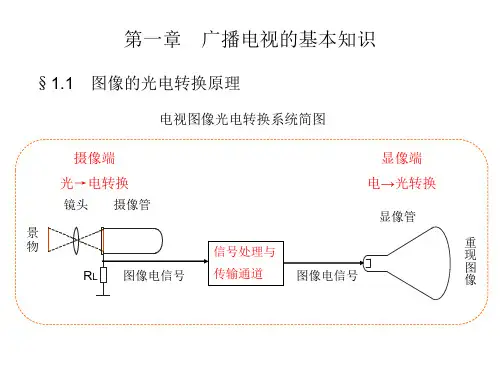
电视机原理图
- 格式:doc
- 大小:78.50 KB
- 文档页数:4
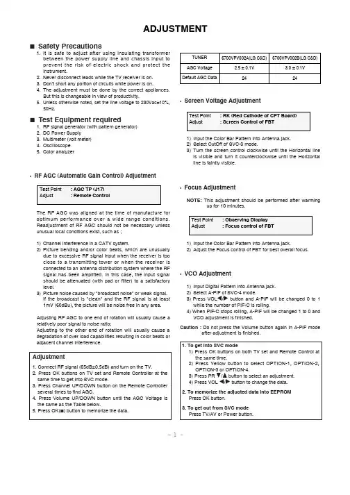
Y Safety Precautions1. It is safe to adjust after using insulating transformerbetween the power supply line and chassis input to prevent the risk of electric shock and protect the instrument.2. Never disconnect leads while the TV receiver is on.3. Don't short any portion of circuits while power is on.4. The adjustment must be done by the correct appliances.But this is changeable in view of productivity.5. Unless otherwise noted, set the line voltage to 230Vac!10%,50Hz.Y Test Equipment required1. RF signal generator (with pattern generator)2. DC Power Supply3. Multimeter (volt meter)4. Oscilloscope5. Color analyzer:RF AGC (Automatic Gain Control) Adjustment The RF AGC was aligned at the time of manufacture for optimum performance over a wide range conditions.Readjustment of RF AGC should not be necessary unless unusual local conditions exist, such as ;1) Channel interference in a CATV system.2) Picture bending and/or color beats, which are unusuallydue to excessive RF signal input when the receiver is too close to a transmitting tower or when the receiver is connected to an antenna distribution system where the RF signal has been amplified. In this case, the input signal should be attenuated (with pad or filter) to a satisfactory level.3) Picture noise caused by "broadcast noise" or weak signal.If the broadcast is "clean" and the RF signal is at least 1mV (60dBu), the picture will be noise free in any area.Adjusting RF AGC to one end of rotation will usually cause a relatively poor signal to noise ratio;Adjusting to the other end of rotation will usually cause a degradation of over load capabilities resulting in color beats or adjacent channel interference. :Screen Voltage Adjustment1) Input the Color Bar Pattern into Antenna jack.2) Select CutOff of SVC-3 mode.3) Turn the screen control clockwise until the Horizontal lineis visible and turn it counterclockwise until the Horizontal line is faintly visible.:Focus AdjustmentNOTE:This adjustment should be performed after warming up for 10 minutes.1) Input the Color Bar Pattern into Antenna jack.2) Adjust the Focus control of FBT for best overall focus.:VCO Adjustment1) Input Digital Pattern into Antenna jack.2) Select A-PIF of SVC-4 mode.3) Press VOL F/G button and A-PIF will be changed 0 to 1while the number of PIF-C is rolling.4) When PIF-C stops rolling, A-PIF will be changed 1 to 0 andVCO adjustment is finished.Caution : Do not press the Volume button again in A-PIF mode after adjustment is finished.ADJUSTMENT-1-:Deflection Data Adjustment (Line SVC-2)1. Preparation for Adjustment1) Select SVC-2 Mode.2) Tune the TV set to receive Digital Pattern and set ARCMode to Standard.2. Initial deflection data and average data for CPT3. Adjustment1) VL(Vertical Linearity) AdjustmentSelect VL adjustment mode to adjust the upper and lower vertical size to be the same for horizontal center line.2) VS(Vertical Shift) AdjustmentAdjust the geometrical horizontal center line of the screen to be coincided with the vertical center line of CPT.3) VA(Vertical Amplitude) AdjustmentAdjust the upper and lower part of big circle of the received pattern to be placed on 6~7mm from the valid screen.4) HS(Horizontal Shift) AdjustmentAdjust the geometrical vertical center line of the received screen to be coincided with the horizontal center line of CPT.5) SC(Vertical S Correction) AdjustmentAdjust the width of upper/center/lower grid of the received pattern to be the same.:SECAM Background Color Adjustment(CT-, CF-) 1. Preparation for AdjustmentSelect ÒS R-YÓ or ÒS B-YÓ of SVC Mode 4.2. AdjustmentWhile switching SECAM and PAL channels in turns, press VOL F/G key until the background color of SECAM channel to be the same as that of PAL Pattern at S R-Y or S B-Y.:White Balance Adjustment.(LINE SVC-1)NOTE :This adjustment should be performed after screen voltage adjustment.1) Tune the TV set to receive 100% white pattern.2) Select SVC-1 Mode.3)Press PR UP/DOWN key to select BG, GG, BG, GC.Adjust BG, GG on Brightness 40!1FL and BG, GC on Brightness 4.5!0.5FL with VOL F/G key to get the color value.4) Adjust BG, GG from the initialized data to get the color value ofX=281!8, Y=288!8.5) R,G,B initial data and average data:Sub Brightness AdjustmentNOTE:This adjustment should be performed after White Balance adjustment.1) Input FUBK pattern to Antenna jack.2) Select S-BRI of SVC-3 mode.3) Press VOL F/G until (a) and (b) of FUBK are distinct andpress VOL G twice more.:OPTION Adjustment (SVC MODE:OPTION-1, OPTION-2)NOTE:When the EEPROM has been replaced, the Option data should be restored as the function of individualsystem and specification.1) Press OK buttons on both TV set and Remote Controller atthe same time to get into SVC mode.2) Press the Yellow button several times to find OPTION-1 orOPTION-2.3) Input the correspond OPTION data referring to Table belowwith the numeric buttons 0~9.StatusRCGCBCGGBGInitial Data1271471235964Remark(a)(b)- 2-- 3-Table 1. OPTION 1 FunctionTable 2. OPTION 2 FunctionSingle SYSTEM(CA-)South East Asian DUAL W/O RF 3.58(CF-,CZ-)W/RF 3.58(CT-,CD-)with RGB InputEYE TOP H-TONE4 KEYSCART CCTV SYSTEMOptionCode 0123010*********FunctionRemarkBG Only BG+TAI DUAL BG+I+DK BG+I+DK+M W/O CCTV W/CCTVPhono Jack or Camera-in Jack Scart Jack6 Key(MENU, OK, VOL-, VOL+, PR-, PR+)4 Key(TV/AV, ROTATE, PR-, PR+)W/O EYE W/EYETeletext Top function Disable Teletext Top function Enable Blue Background OSD MENU Half Tone OSD MENULG8993-27A/BLG8993-28A LG8993-29A CURVETBS HOTELLANG-INDEXLANG.Option Code 0 00 11 00123401234501234010101FunctionRemarkMulti English Only TWO Lang.English CIS China Romania Poland English France Hindi Arab Urdu Parsi English Indonesia Malay Vietnam ThaiFast Volume Curve Slow Volume Curve TBS Function Disable TBS Function Enable HOTEL Function Disable HOTEL Function EnableTROUBLESHOOTING1. No Power (Not working SMPS)2. No Power On (SMPS working)8. No TeletextBLOCK DIAGRAMPRINTED CIRCUIT BOARD MAINEXPLODED VIEW(CT-14G29)-1-- 2-EXPLODED VIEW PARTS LISTREPLACEMENT P ARTS LISTFor Capacitor & Resistors, the charactors at 2nd and 3rd digit in the P/No. means as follows;CC, CX, CK, CN : Ceramic CQ : Polyestor CE : ElectrolyticRD : Carbon FilmRS : Metal Oxide Film RN : Metal Film RF : FusibleLOCA. NO PART NO DESCRIPTIONC18 C19 C20 C22 C23C24C25C26C27 C28 C29C30 C91 C100 C101 C102 C103 C104 C106 C107 C108 C109 C112 C113 C114 C115 C151 C152 C153 C154 C155 C156 C157 C159 C162 C201 C202C205 C221 C222 C223 C225 C226 C227 C258 C292 C293 C294 C295 C301 C303 C304 0CN2210K5190CN1030F6790CE108DD6180CX5600K4090CX5600K4090CE106DK6180CE106DK6180CE106DK6180CN1040K9490CN1040K9490CN1040K9490CE106DF6180CN2210K5190CN1030F6790CN1030F6790CN1040K9490CE105DK6180CE107DD6180CN1030F6790CX5600K4090CX5600K4090CE106DK6180CE475DK6180CN1030F6790CN1030F6790CN1030F6790CE106DK6180CN1040K9490CX4700K4090CX3900K4090CN3310K5190CX5600K4090CX5600K4090CN1040K9490CN3320F5690CE226DF6180CX3900K4090CQ1531N5090CE476DF6180CE106DK6180CE106DK6180CX5100K4090CX5100K4090CE106DK6180CE106DK6180CN1030F6790CN1030F6790CN1010K5190CN1010K519181-007H0CK4710W5150CK4710W515220P 50V K10000P 16V M1000UF STD 10V M56P 50V J56P 50V J10UF STD 50V M10UF STD 50V M10UF STD 50V M0.1M 50V Z0.1M 50V Z0.1M 50V Z10UF STD 16V M220P 50V K10000P 16V M10000P 16V M0.1M 50V Z1UF STD 50V M100UF STD 10V M10000P 16V M56P 50V J56P 50V J10UF STD 50V M4.7000UF STD 50V M10000P 16V M10000P 16V M10000P 16V M10UF STD 50V M0.1M 50V Z47P 50V J39P 50V J330P 50V K56P 50V J56P 50V J0.1M 50V Z3300P 16V K22UF STD 16V M39P 50V J0.015U 100V K47UF STD 16V M10UF STD 50V M10UF STD 50V M51P 50V J51P 50V J10UF STD 50V M10UF STD 50V M10000P 16V M10000P 16V M100P 50V K100P 50V KECQ-V1H474JZ3(TR),50V 0.4470PF 500V K470PF 500V KLOCA. NO PART NO DESCRIPTIONC305C306C307C308C309C310C311C312C313C314C315C402C404C405C406C408C412Ò(20Ó)Ò(21Ó)C413C414Ò(20Ó)C418C501C502C503C504C505C506C507C508C509C510C511C512C513C514C515C516C517C518Ò(20Ó)C519C520C521C522C525C526C527C528C529C5300CN1020K5190CN1020K5190CE107DJ6180CN1020K5190CE477DJ6180CQ1041N5090CE228DJ61A0CQ1041N509181-007T0CQ6831N5090CE474DK618181-091V0CQ1531N5090CE476DF6180CN1030F6790CE106DK618181-013C181-013P181-013B0CK2220W515181-015E181-015F181-009R0CQ3321N5090CQ2221N5090CE224DK6180CX1100K4090CN1020K5190CN1040K9490CE227DF6180CE337DF6180CN1030F6790CE107DD6180CE226DF6180CE105DK618181-007F0CE337DF6180CN1030F6790CE107DD6180CE105DK6180CQ4721N5090CQ3921N4090CE474DK6180CN1030F6790CE476DF6180CN1030F679181-007H181-007F0CE106DK6180CX5600K4090CX5600K4090CE105DK6181000P 50V K1000P 50V K100UF STD 35V M1000P 50V K470UF STD 35V M0.1U 100V K2200UF STD 35V M0.1U 100V KECQ-V1H105JZ3(TR),50V 1.00.068U 100V K0.4700UF STD 50V M2KV R 391K TP7.50.015U 100V K47UF STD 16V M10000P 16V M10UF STD 50V MMPP 200V 0.39UF JMPP 400V 0.33UF JMPP 200V 0.36UF J2200P 500V K BMPP 1600V 0.0068UF HMPP 1600V 0.0073UF HPP 200V 0.022UF K0.0033U 100V K0.0022U 100V K0.2200UF STD 50V M11P 50V J1000P 50V K0.1M 50V Z220UF STD 16V M330UF STD 16V M10000P 16V M100UF STD 10V M22UF STD 16V M1UF STD 50V MECQ-V1H224JZ3(TR),50V 0.2330UF STD 16V M10000P 16V M100UF STD 10V M1UF STD 50V M0.0047U 100V K0.0039U 100V J0.4700UF STD 50V M10000P 16V M47UF STD 16V M10000P 16V MECQ-V1H474JZ3(TR),50V 0.4ECQ-V1H224JZ3(TR),50V 0.210UF STD 50V M56P 50V J SL56P 50V J SL1UF STD 50V MFor Capacitor & Resistors, the charactors at 2nd and 3rd digit in the P/No. means as follows;CC, CX, CK, CN : CeramicCQ : PolyestorCE : ElectrolyticRD : Carbon FilmRS : Metal Oxide FilmRN : Metal FilmRF : FusibleFor Capacitor & Resistors, the charactors at 2nd and 3rd digit in the P/No. means as follows;CC, CX, CK, CN : Ceramic CQ : Polyestor CE : ElectrolyticRD : Carbon FilmRS : Metal Oxide Film RN : Metal Film RF : FusibleLOCA. NO PART NO DESCRIPTIONR40Ò R44 R45 R46 R47 R51 R52 R54 R55 R56 R57 R58 R59 R60 R63R64 R100 R101 R102 R103 R104 R105 R106 R107 R110 R130 R151 R152 R153 R154 R155 R156 R157 R158 R161 R164 R165 R166 R167 R168 R169 R170 R171 R172 R201Ò R202 R203R204R205 R206 0RD5101F6090RD7501F6090RD4701F6090RD1002F6090RD4701F6090RD1000F6090RD4701F6090RD4701F6090RD1000F6090RD1000F6090RD4701F6090RD4701F6090RD4701F6090RD4701F6090RD4701F6090RD4701F6090RD1001F6090RD0392F6090RD1201F6090RD2701F6090RD0272F6090RD1000F6090RD1000F6090RD1201F6090RD0562F6090RS0392K6070RD2200F6090RD1000F6090RD1000F6090RD0102F6090RD1501F6090RD9101F6090RD4700F6090RD3301F6090RD3900F6090RD3900F6090RD2200F6090RD2200F6090RD2200F6090RD2200F6090RD1002F6090RD1002F6090RD1001F6090RD1001F6090RD1002F6090RD0682F6090RD0562F6090RD4700F6090RD3600F6090RD0752F6090RD0752F6090RD5101F6095.1K 1/6W 5 TA527.5K 1/6W 5 TA524.70K 1/6W 5% TA5210K 1/6W 5 TA524.70K 1/6W 5% TA52100 1/6W 5 TA524.70K 1/6W 5% TA524.70K 1/6W 5% TA52100 1/6W 5 TA52100 1/6W 5 TA524.70K 1/6W 5% TA524.70K 1/6W 5% TA524.70K 1/6W 5% TA524.70K 1/6W 5% TA524.70K 1/6W 5% TA524.70K 1/6W 5% TA521K 1/6W 5% TA5239 1/6W 5% TA1.2K 1/6W 5 TA522.7K 1/6W 5 TA5227 1/6W 5 TA52100 1/6W 5 TA52100 1/6W 5 TA521.2K 1/6W 5 TA5256 1/6W 5% TA5239 2W 5% TA62220 1/6W 5 TA52100 1/6W 5 TA52100 1/6W 5 TA5210 1/6W 5 TA521.5K 1/6W 5 TA529.1K 1/6W 5 TA52470 1/6W 5 TA523.3K 1/6W 5 TA52390 1/6W 5 TA52390 1/6W 5 TA52220 1/6W 5 TA52220 1/6W 5 TA52220 1/6W 5 TA52220 1/6W 5 TA5210K 1/6W 5 TA5210K 1/6W 5 TA521.0K 1/6W 5 TA521.0K 1/6W 5 TA5210K 1/6W 5 TA5268 1/6W 5 TA5256 1/6W 5 TA52 *SCART470 1/6W 5 TA52360 1/6W 5 TA5275 1/6W 5 TA5275 1/6W 5 TA525.1K 1/6W 5 TA52For Capacitor & Resistors, the charactors at 2nd and 3rd digit in the P/No. means as follows;CC, CX, CK, CN : CeramicCQ : PolyestorCE : ElectrolyticRD : Carbon FilmRS : Metal Oxide FilmRN : Metal FilmRF : FusibleLOCA. NO PART NO DESCRIPTIONR207R208 R209 R210R211 R212 R213 R214 R215 R221Ò R222 R223 R224 R226 R228Ò R240 R250 R290 R291 R303 Ò(20Ó) Ò(21Ó) R304 Ò(21Ó) R305 R306 R309 Ò(20Ó) Ò(21Ó) R310 R311 Ò(21Ó) R312 R313 R314 R315 R402 R403 R405 Ò(20Ó) R407 Ò(21Ó) R409 R410 Ò(20Ó) Ò(21Ó) R411 R412 R413 R414 0RD0752F6090RD0752F6090RD1001F6090RD0101F6090RD4302F6090RD6200F6090RD1002F6090RD1001F6090RD1203F6090RD3000F6090RD2000F6090RD1201F6090RD1001F6090RD6202F6090RD1001F6090RD1801F6090RD1201F6090RD0752F6090RD1001F6090RD2200H6090RD2200H6090RD0471H6090RD0391H6090RD0331H6090RD0471H6090RD0391H6090RD5102F6090RD4701F6090RD5101H6090RD1201H6090RD3001H6090RD0221H6090RD1501F6090RD1201F6090RD1001F6090RD8202F6090RD9100F6090RD3900H6090RS1002H6090RD5100H6090RS0822J6070RS0472J6070RS1202J6070RS1502J6070RD0332H6090RD1303H6090RD1003H6090RD9102H6090RD4700F6090RD3600F6090RD3300H6090RD1502F60975 1/6W 5 TA5275 1/6W 5 TA521.0K 1/6W 5 TA521.0 1/6W 5 TA5243K 1/6W 5 TA52620 1/6W 5 TA5210K 1/6W 5 TA521.0K 1/6W 5 TA52120K 1/6W 5 TA52300 1/6W 5 TA52200 1/6W 5 TA521.2K 1/6W 5 TA521.0K 1/6W 5 TA5262K 1/6W 5 TA521.0K 1/6W 5 TA521.8K 1/6W 5 TA521.2K 1/6W 5 TA52 *SCART75 1/6W 5% TA1K 1/6W 5% TA220 1/2W 5% TA220 1/2W 5% TA4.7 1/2W 5 TA523.9 1/2W 5 TA523.3 1/2W 5 TA524.7 1/2W 5 TA523.9 1/2W 5 TA5251K 1/6W 5 TA524.70K 1/6W 5% TA525.1K 1/2W 5 TA521.2K 1/2W 5 TA523K 1/2W 5 TA522.2 1/2W 5 TA521.5K 1/6W 5 TA521.2K 1/6W 5 TA521.0K 1/6W 5 TA5282K 1/6W 5 TA52910 1/6W 5 TA52390 1/2W 5 TA5210K 1/2W 5 TA52510 1/2W 5 M1582OHM 1 W 5% TA6247 1 W 5% TA6212K 1W 5% TA6215K 1W 5% TA6233 1/2W 5 TA52130K 1/2W 5 TA52100K 1/2W 5 TA5291K 1/2W 5 TA52470 1/6W 5 TA52360 1/6W 5 TA52330 1/2W 5 TA5215K 1/6W 5 TA52LOCA. NO PART NO DESCRIPTIONR418R501R502R503R504R505R506R507R508R509R510R511R512R513R514R515R516R517R518R519R520R521R522R523R524R525R526R527R528R529R530R531R532R533R535R536R538R539R540R541R542R544R548R549R550R551R552R554R555R556R561R5620RD1200F6090RD3002F6090RD1000F6090RD1000F6090RD1000F6090RD3302F6090RD1000F6090RD1000F6090RD1001F6090RD1001F6090RD4701F6090RD5100F6090RD2202F6090RD5600F6090RD4703F6090RD1000F6090RD2201F6090RD3002F6090RD1302F6090RD1502F6090RD1202F6090RD1000F6090RD1002F6090RD0102F6090RD1000F6090RD6801F6090RD2201F6090RD1000F6090RD2200F6090RD0752F6090RD1000F6090RS0682J6070RD3902F6090RD3900F6090RD2200F6090RD2201F6090RD5102F6090RD1002F6090RD1002F6090RD2001F6090RD1001F6090RD1002F6090RD1002F6090RD1001F6090RD2001F6090RD2001F6090RD2001F6090RS0472H6090RD2203H6090RD1504F6090RD1001F6090RD6201F609120 1/6W 5 TA5230K 1/6W 5 TA52100 1/6W 5 TA52100 1/6W 5 TA52100 1/6W 5 TA5233K 1/6W 5% TA52100 1/6W 5 TA52100 1/6W 5 TA521.0K 1/6W 5 TA521.0K 1/6W 5 TA524.70K 1/6W 5% TA52510 1/6W 5 TA5222K 1/6W 5 TA52560 1/6W 5 TA52470K 1/6W 5 TA52100 1/6W 5 TA522.2K 1/6W 5 TA5230K 1/6W 5 TA5213K 1/6W 5 TA5215K 1/6W 5 TA5212K 1/6W 5 TA52100 1/6W 5 TA5210K 1/6W 5 TA5210 1/6W 5 TA52100 1/6W 5 TA526.8K 1/6W 5 TA522.2K 1/6W 5 TA52100 1/6W 5 TA52220 1/6W 5 TA5275 1/6W 5% TA100 1/6W 5 TA5268 1W 5% TA6239K 1/6W 5 TA52390 1/6W 5 TA52220 1/6W 5 TA522.2K 1/6W 5 TA5251K 1/6W 5 TA5210K 1/6W 5 TA5210K 1/6W 5 TA522.0K 1/6W 5 TA521.0K 1/6W 5 TA5210K 1/6W 5 TA5210K 1/6W 5 TA521.0K 1/6W 5 TA522.0K 1/6W 5 TA522.0K 1/6W 5 TA522.0K 1/6W 5 TA5247 1/2W 5 TA52220K 1/2W 5 TA521.5M 1/6W 5 TA521.0K 1/6W 5 TA526.2K 1/6W 5 TA52For Capacitor & Resistors, thecharactors at 2nd and 3rd digitin the P/No. means as follows;CC, CX, CK, CN : CeramicCQ : PolyestorCE : ElectrolyticRD : Carbon FilmRS : Metal Oxide FilmRN : Metal FilmRF : FusibleFor Capacitor & Resistors, the charactors at 2nd and 3rd digit in the P/No. means as follows;CC, CX, CK, CN : Ceramic CQ : Polyestor CE : ElectrolyticRD : Carbon FilmRS : Metal Oxide Film RN : Metal Film RF : Fusible。