
2302-1-01-01-00-00-07-0中文资料
- 格式:pdf
- 大小:59.38 KB
- 文档页数:1

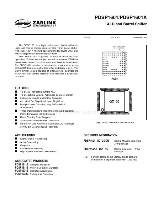
PDSP1601/PDSP1601A 1The PDSP1601 is a high performance 16-bit arithmetic logic unit with an independent on-chip 16-bit barrel shifter.The PDSP1601A has two operating modes giving 20MHz or 10MHz register-to-register transfer rates.The PDSP1601 supports Multicycle multiprecision operation. This allows a single device to operate at 20MHz for 16-bit fields, 10MHz for 32-bit fields and 5MHz for 64-bit fields.The PDSP1601 can also be cascaded to produce wider words at the 20MHz rate using the Carry Out and Carry In pins. The Barrel Shifter is also capable of extension, for example the PDSP1601 can used to select a 16-bit field from a 32-bit input in 100ns.APPLICATIONS s Digital Signal Processing s Array Processing s Graphicss Database AddressingsHigh Speed Arithmetic ProcessorsFEATURESs 16-bit, 32 instruction 20MHz ALUs 16-bit, 20MHz Logical, Arithmetic or Barrel Shifter s Independent ALU and Shifter Operation s 4 x 16-bit On Chip Scratchpad Registers s Multiprecision Operation; e.g. 200ns 64-bit Accumulates Three Port Structure with Three Internal Feedback Paths Eliminates I/O Bottlenecks s Block Floating Point Supports 300mW Maximum Power Dissipations84-pin Pin Grid Array or 84 Contact LCC Packages or 100 pin Ceramic Quad Flat PackASSOCIATED PRODUCTSPDSP16112Complex MultiplierPDSP1611616 x 16 Complex Multiplier PDSP16318Complex Accumulator PDSP16330Pythagoras ProcessorFig.1 Pin connections - bottom viewORDERING INFORMATIONPDSP1601 MC GGCR 10MHz MIL883 Screened -QFP packagePDSP1601A BO AC 20MHz Industrial - PGA packageN.BFurther details of the Military grade part are available in a separate datasheet (DS3763)PDSP1601/PDSP1601AALU and Barrel ShifterDS3705ISSUE 3.0November 1998PDSP1601/PDSP1601A2FunctionGNDC8C9C10C11C12C13C14C15OEBFPVCCCORA0RA1RA2CIIA0IA1IA2IA3AC pinF9F11E11E10E9D11D10C11B11C10A11B10B9A10A9B8A8B6B7A7C7AC pinJ6J7L7K7L6L8K8L9L10K9L11K10J10K11J11H10H11F10G10G11G9FunctionIS0IS1IS2IS3SV0SV1SV2SV3SVOERS0RS1VCCRS2C0C1C2C3C4C5C6C7AC pinF3G3G1G2F1H1H2J1K1J2L1K2K3L2L3K4L4J5K5L5K6FunctionGNDMSA0MSA1A15A14A13A12A11A10A9A8A7A6A5A4A3A2A1A0CEAMSCAC pinC6A6A5B5C5A4B4A3A2B3A1B2C2B1C1D2D1E3E2E1F1PIN DESCRIPTIONFunctionIA4MSBMSSB15B14B13B12B11B10B9B8B7B6B5B4B3B2B1B0CEBCLKGC51525354555657585960616263646566676869707172737475GC26272829303132333435363738394041424344454647484950SIGN/CN/CN/CN/CVCCC0RA0RA1RA2CIIA0IA1IA2IA3IA4MSBMSSB15B14B13B12B11B10B9B8SIGN/CN/CN/CN/CB7B6B5B4B3B2B1B0CEBCLKGNDMSA0MSA1A15A14A13A12A11A10A9A8SIGN/CN/CN/CN/CA7A6A5A4A3A2A1A0CEAMSCIS0IS1IS2IS3SV0SV1SV2SV3SVOERS0RS1GC767778798081828384858687888990919293949596979899100SIGN/CN/CN/CN/CVCCRS2C0C1C2C3C4C5C6C7GNDC8C9C10C11C12C13C14C15OEBFP GC12345678910111213141516171819202122232425N/C = not connected - leave open circuitAll GND and VDD pin must be usedhttps://PDSP1601/PDSP1601A3Symbol MSB MSS B15 - B0CEB CLKMSA0 - MSA1A15 - A0CEA MSC IS0 - IS3SV0 - SV3SVOERS0, RS1RS2C0 - C15OE BFP CO RA0 - RA2CI IA0 - IA3IA4Vcc GND DescriptionALU B-input multiplexer select control.1 This input is latched internally on the rising edge of CLK.Shifter Input multiplexer select control.1 This input is latched internally on the rising edge of CLK.B Port data input. Data presented to this port is latched into the input register on the rising edge of CLK. B15 is the MSB.Clock enable, B Port input register. When low the clock to this register is mon clock to all internal registered elements. All registers are loaded, and outputs change on the rising edge of CLK.ALU A-input multiplexer select control.1 These inputs are latched internally on the rising edge of CLK.A Port data input. Data presented to this port is latched into the input register on the rising edge of CLK. A15 is the MSB.Clock enable, A Port input register. When low the clock to this register is enabled.C-Port multiplexer select control.1 This input is latched internally on the rising edge of CLK.Instruction inputs to Barrel Shifter, IS3 = MSB.1 These inputs are latched internally on the rising edge of CLK.Shift Value I/O Port. This port is used as an input when shift values are supplied fromexternal sources, and as an output when Normalise operations are invoked. The I/O functions are determined by the IS0 - IS3 instruction inputs, and by the SVOE control.The shift value is latched internally on the rising edge of CLK.SV Output enable. When high the SV port can only operate as an input. When low the SV port can act as an input or as an output, according to the IS0 - IS3 instruction. This pin should be tied hihg or low, depending upon the application.Instruction inputs to Barrel Shifter registers.1 These inputs are latched internally on the rising edge of CLK.C Port data output. Data output on this port is selected by the C output multiplexer.C15 is the MSB.Output enable. The C Port outputs are in high impedance condition when this control is high.Block Floating Point Flag from ALU, active high.Carry out from MSB of ALU.Instruction inputs to ALU registers.1 These inputs are latched internally on the rising edge of CLK.Carry in to LSB of ALU.Instruction inputs to ALU.1 IA4 = MSB. These inputs are latched internally on the rising edge of CLK.+5V supply: Both Vcc pins must be connected.0V supply: Both GND pins must be connected.PIN DESCRIPTIONSNOTES1. All instructions are executed in the cycle commencing with the rising edge of the CLK which latches the inputs.https://PDSP1601/PDSP1601A4FUNCTIONAL DESCRIPTIONThe PDSP1601 contains four main blocks: the ALU, the Barrel Shifter and the two Register Files.The ALUThe ALU supports 32 instructions as detailed in Table 1.The inputs to the ALU are selected by the A and B MUXs.Data will fall through from the selected register through the A or B input MUXs and the ALU to the ALU output register file in 50ns for the PDSP1601A (100ns for the PDSP1601).The ALU instructions are latched, such that the instruction will not start executing until the rising edge of CLK latches the instruction into the device.The ALU accepts a carry in from the CI input and supplies a carry out to the CO output. Additionally, at the end of each cycle, the carry out from the ALU is loaded into an internal 1bit register, so that it is available as an input to the ALU on the next cycle. In the manner, multicycle, multiprecision operations are supported. (See MULTICYCLE CASCADE OPERATIONS).BFP FlagThe ALU has a user programmable BFP flag. This flag may be programmed to become active at any one of four conditions. Two of these conditions are intended to support Block Floating Point operations, in that they provide flags indicating that the ALU result is within a factor of two or four of overflowing the 16 bit number range. For multiprecision operations the flag is only valid whilst the most significant 16bit byte is being processed. In this manner the BFP flag may be used over any extended word width.The remaining two conditions detect either an overflow condition or a zero result. For the overflow condition to beactive the ALU result must have overflowed into the 16th (sign)bit, (this flag is only valid whilst the most significant 16 bit byte is being processed). The zero condition is active if the result from the ALU is equal to zero. For multiprecision operations the zero flag must be active for all of the 16 bit bytes of an extended word.The BFP flag is programmed by executing on of the four SBFXX instructions (see Table 1). During the execution of any of these four instructions, the output of the ALU is forced to zero.Multicycle/Cascade OperationThe ALU arithmetic instructions contain two or three options for each arithemtic operation.The ALU is designed to operate with two's complement arithmetic, requiring a one to be added to the LSB for all subtract operations. The instructions set includes instructions that will force a one into the LSB, e.g. MIAX1, AMBX1, BMAX1(see Table 1).These instructions are used for the least significant 16 bit byte of any subtract operation.The user has an option of cascading multiple devices, or multicycling a single device to extend the arithmetic precision.Should the user cascade multiple devices, then the cascade arithmetic instructions using the external CI input should be employed for all but the least significant 16 bit byte, e.g. MIACI,APBCI, BMACI (see Table 1).Should the user multicycle a single device, then the Multicycle Arithmetic instructions, using the internally registered CO bit should be employed for all but the least significant 16 bit byte, e.g. MIACO, APBCO, AMBCO,BMACO (see Table 1).Fig.2 PDSP1601 block diagramhttps://PDSP1601/PDSP1601A5Inst 000102030405060708090A 0B 0C 0D 0E 0FIA4-AI000000000010001000011001000010100110001110100001001010100101101100011010111001111Mnemonic CLRXX MIAX1MIACI MIACO A2SGN A2RAL A2RAR A2RSX APBCI APBCO AMBX1AMBCI AMBCO BMAX1BMACI BMACOOperation RESET MINUS A MINUS A MINUS A A/2A/2A/2A/2A PLUSB A PLUS B A MINUS B A MINUS B A MINUS B B MINUS A B MINUS A B MINUS AMode ---------LSBYTE CASCADE MULTICYCLE MSBYTE MULTICYCLE MULTICYCLE MULTICYCLE CASCADE MULTICYCLE LSBYTE CASCADE MULTICYCLE LSBYTE CASCADE MULTICYCLEFunctionCLEAR ALL REGISTERS NA Plus 1NA Plus CI NA Plus CO A/2 Sign Extend A/2 with RAL LSB A/2 with RAR LSB A/2 with RSX LSB A Plus B Plus CI A Plus B Plus CO A Plus NB Plus 1A Plus NB Plus CI A Plus NB Plus CO NA Plus B Plus 1NA Plus B Plus CI NA Plus B Plus COTable 1 ALU instructions1a. ARITHMETIC INSTRUCTIONSInst 1011121314151617IA4-AI01000010001100101001110100101011011010111Mnemonic ANXAB ANANB ANNAB ORXAB ORNAB XORAB PASXA PASNAOperation A AND B A AND NB NA AND B A OR B NA OR B A XOR B PASS A INVERT AFunction A. B A. NB NA. B A + B NA + B A XOR B A NA1c. CONTROL INSTRUCTIONSInst 18191A 1B 1C 1D 1E 1FIA4-AI01100011001110101101111100111011111011111Mnemonic SBFOV SBFU1SBFU2SBFZE OPONE OPBYT OPNIB OPALTOperationSet BFP Flag to OVR, Force ALU output to zero Set BFP Flag to UND 1 Force ALU output to zero Set BFP Flag to UND 2 Force ALU output to zero Set BFP Flag to ZERO Force ALU output to zero Output 0001 Hex Output 00FF Hex Output 000F Hex Output 5555 HexKEY A = A input to ALU B = B input to ALUCI = External Carry in to ALUCO = Internally Registered Carry out from ALU RAL = ALU Register (Left)RAR = ALU Register (Right)RSX= Shifter Register (Left or Right)MNEMONICSCLRXX Clear All Registers to zero MIAXX Minus A,XX = Carry in to LSB A2XXX A Divided by 2,XXX = Source of MSB APBXX A Plus B,XX = Carry in to LSB AMBXX A Minus B,XX = Carry in to LSB BMAXX B Minus A,XX = Carry in to LSB ANX-Y AND X = Operand 1, Y = Operand 2ORX-Y OR X = Operand 1, Y = Operand 2XORXY Exclusive OR X = Operand 1, Y = Operand 2PASXX Pass XX = Operand SBFXX Set BFP Flag XX = Function OPXXXOutput Constant XXX1b. LOGICAL INSTRUCTIONShttps://PDSP1601/PDSP1601A6Divide by TwoThe ALU has four (A2SGN, A2RAL, A2RAR, A2RSX)instructions used for right shifting (dividing by two) extended precision words. These words, (up to 64 bits) may be stored in the two on-chip register files. When the least significant 16bit word is shifted, the vacant MSB must be filled with the LSB from the next most significant 16 bit byte. This is achieved via the A2RAL, A2RAR or A2RSX instructions which indicate the source of the new MSB (see ALU INSTRUCTION SET).When the most significant 16 bit byte is right shifted, the MSB must be filled with a duplicate of the original MSB so as to maintain the correct sign (Sign Extension). This operation is achieved via the A2SGN instruction (see Table 1).ConstantsThe ALU has four instructions (OPONE, OPBYT, OPNIB,OPALT) that force a constant value onto the ALU output.These values are primarily intended to be used as masks, or the seeds for mask generation, for example, the OPONE instruction will set a single bit in the least significant position.This bit may be rotated any where in the 16 bit field by the Barrel Shifter, allowing the AND function of the ALU to perform bit-pick operations on input data.CLRThe ALU instruction CLRXX is used as a Master Reset for the entire device. This instruction has the effect of:1.Clearing ALU and Barrel Shifter register files to zero.2.Clearing A and B port input registers to zero.3.Clearing the R1 and R2 shift control registers to zero.4.Clearing the internally registered CO bit to zero.5.Programming the BFP flag to detect overflow conditions.The Barrel ShifterThe Barrel Shifter supports 16 instructions as detailed in Table 2. The input to the Barrel Shifter is selected by the S MUX. Data will fall through from the selected register, through the S MUX and the Barrel Shifter to the shifter output register file in 50ns for the PDSP1601A (100ns for the PDSP1601).The Barrel Shifter instructions are latched, such that the instructions will not start executing until the rising edge of CLK latches the instruction into the device.The Barrel Shifter is capable of Logical Arithmetic or Barrel Shifts in either direction.A.Logical shifts discard bits that exit the 16 bit field and fill spaces with zeros.B.Arithmetic shifts discard bits that exit the 16 bit field and fill spaces with duplicates of the original MSB.C.Barrel Shifts rotate the 16 bit fields such that bits tha exit the 16 bit field to the left or right reappear in the vacant spaces on the right or left.The amount of shift applied is encoded onto the 4 bit Barrel Shifter input as illustrated in Table 3. The type of shift and the amount are determined by the shift control block. The shift control block (see Fig.3) accepts and decodes the four bit ISO-3 instruction. The shift control block contains a priority encoder and two user programmable 4 bit registers R1 and R2.There are four possible sources of shift value that can be passed onto the Barrel Shifter, there are:1.The Priority Encoder 2.The SV input 3.The R1 register 4.The R2 register Mnemonic LSRSV LSLSV BSRSV BSLSV LSRR1LSLR1LSRR2LSLR2LR1SV LR2SV ASRSV ASRR1ASRR2NRMXX NRMR1NRMR2IS3-IS00000000100100011010001010110011110001001101010111100110111101111OperationLogical Shift Right by SV Logical Shift Left by SV Barrel Shift Right by SV Barrel Shift Left by SV Logical Shift Right by R1Logical Shift Left by R1Logical Shift Right by R2Logical Shift Left by R2Load Register 1 From SV Load Register 2 From SV Arithmetic Shift Right by SV Arithmetic Shift Right by R1Arithmetic Shift Right by R2Normalise Output PENormalise Output PE, Load R1Normalise Output PE, Load R2Inst 0123456789A B C D E FI/O I I I I X X X X I I I X X O O OTable 2 Barrel shifter instructionsKEY SV = Shift Value R1= Register 1R2= Register 2PE = Priority Encoder OutputI => SV Port operates as an Input O => SV Port operates as an Output X=> SV Port in a High Impedance StateMNEMONICSLSXYY Logical Shift,X = Direction YY = Source of Shift Value BSXYY Barrel Shift,X = Direction YY = Source of Shift Value ASXYY Arithmetic Shift,X = Direction YY = Source of Shift Value LXXYY Load XX = Target YY = SourceNRMYYNormalise by PE, Output PE value on SV Port, Load YY Reghttps://PDSP1601/PDSP1601A7SV30000000011111111SV20000111100001111SV10011001100110011SV00101010101010101Shift No shift 1 place 2 places 3 places 4 places 5 places 6 places 7 places 8 places 9 places 10 places 11 places 12 places 13 places 14 places 15 places(1)Priority encode the 16 bit input to the Barrel Shifter and place the 4 bit value in either of the R1 or R2 registers and output the value on the SV port (if enabled by SVOE ).(2)Shift the 16 bit input by the amount indicated by the Priority Encoder such that the output from the Barrel Shifter is a normalised value.SV InputIf the SV port is selected as the source of the shift value,then the input to the Barrel Shifter is shifted by the value stored in the internal SV register.SVOEThe SV port acts as an input or an output depending upon the IS0-3 instruction. If the user does not wish to use the normalise instructions, then the SV port mat be forced to be input only by typing SVOE control high. In this mode the SV port may be considered an extension of the instruction inputs.R1 and R2 RegistersThe R1 and R2 registers may be loaded from the Priority Encoder (NRMR1 and NRMR2) or from the SV input (LR1SV,LR2SV).Whilst the latter two instructions are executing, the Barrel Shifter will pass its input to the output unshifted.Priority EncoderIf the priority encoder is selected as the source of the shift value (instructions:- NRMXX, NRMR1, MRMRZ), then within one 100ns cycle or two 50ns cycles for the PDSP1601A (one 200ns or two 100ns cycles for the PDSP1601), the shift circuitry will:Table 3 Barrel shifter codesFig.3 Shift control blockhttps://PDSP1601/PDSP1601A8The Register FilesThere are two on-chip register files (ALU and Shifter), each containing two 16 bit registers and each supporting 8instructions (see Table 4). The instructions for the ALU register file and the Barrel Shifter Register file are the same.The Inputs to the register files come from either the ALU or the Barrel Shifter, and are loaded into the Register files on the rising edge of CLK.The register file instructions are latched such that the instruction will not start executing until the rising edge of theCLK latches the instruction into the device.The register file instructions (see Table 4) allow input data to be loaded into either, neither or both of the registers. Data is loaded at the end of the cycle in which the instruction is executing.The register file instructions allow the output to be sourced from either of the two registers, the selected output will be valid during the cycle in which the instruction is executing.OperationLoad Left Reg Output Right Reg Load Right Reg Output Left Reg Load Left Register, Output Left Reg Load Right Register, Output Right Reg Load Both Registers, Output Left Reg No Load Operation, Output Right Reg No Load Operation, Output Left RegNo Load Operation, Pass Barrel Shifter ResultOperationLoad Left Reg Output Right Reg Load Right Reg Output Left Reg Load Left Register, Output Left Reg Load Right Register, Output Right Reg Load Both Registers, Output Left Reg No Load Operation, Output Right Reg No Load Operation, Output Left Reg No Load Operation, Pass ALU ResultInst 01234567RA2-RA0000001010011100101110111Mnemonic LLRRR LRRLR LLRLR LRRRR LBRLR NOPRR NOPLR NOPPSALU REGISTER INSTRUCTIONSInst 01234567RA2-RA0000001010011100101110111Mnemonic LLRRR LRRLR LLRLR LRRRR LBRLR NOPRR NOPLR NOPPSSHIFTER REGISTER INSTRUCTIONSTable 4 ALU and shift register instructions mnemonicsMNEMONICSLXXYY Load XX = Target,YY = Source of Output LBOXX Load Both Registers,XX = Source of Output NOPXX No Load Operation,XX= Source of Outputhttps://PDSP1601/PDSP1601A9MARAX MAAPR MABPR MARSXMultiplexersThere are four user selectable on-chip multiplexers (A-MUX, B-MUX, S-MUX and C-MUX).These four multiplexers support instructions as tabulated in Table 5.The MUX instructions are latched such that the instruction will not start executing until the rising edge of CLK latches the instruction onto the device.MSA10011A-MUXOutputALU REGISTER FILE OUPUT A-PORT INPUT B-PORT INPUTSHIFTER REGISTER FILE OUTPUTMSB01B-MUXOutputB-PORT INPUTSHIFTER REGISTER FILE OUTPUTMSS01S-MUXOutputB-PORT INPUTSHIFTER REGISTER FILE OUTPUTMSC01C-MUXOutputALU REGISTER FILE OUTPUTSHIFTER REGISTER FILE OUTPUTTable 5MSA00101https://PDSP1601/PDSP1601A10INSTRUCTION SETALU Arithmetic Instructions FunctionOn the rising edge of CLK at the end of the cycle in which this instruction is executing, the A Port, B Port, ALU, Barrel Shifter, and Shift Control Registers will be loaded with zeros.The internal registered CO will also be set to zero, and the BFP flag will be set to activate on overflow conditions.The A input to the ALU is inverted and a one is added to the LSB.The A input to the ALU is inverted and the CI input is added to the LSB.The A input to the ALU is inverted and the CO output from the ALU on the previous cycle is added to the LSB.The A input to the ALU is right shifted one bit position. The LSB is discarded, and the vacant MSB is filled by duplicating the original MSB (Sign Extension).The A input to the ALU is right shifted one bit position. The LSB is discarded, and the vacant MSB is filled with the LSB from the ALU register.The A input to the ALU is right shifted one bit position. The LSB is discarded, and the vacant MSB is filled with the LSB from the ALU register.The A input to the ALU is right shifted one bit position. The LSB is discarded, and the vacant MSB is filled with the LSB from the B input to the ALU.The A input to the ALU is added to the B input, and the CI input is added to the LSB.The A input to the ALU is added to the B input, and the CO out from the ALU on the previous cycle is added to the LSB.The A input to the ALU is added to the inverted B input, and a one is added to the LSB.The A input to the ALU is added to the inverted B input, and the CI input is added to the LSB.The A input to the ALU is added to the inverted B input, and the CO out from the ALU on the previous cycle is added to the LSB.The inverted A input to the ALU is added to the B input, and a one is added to the LSB.The inverted A input to the ALU is added to the B input, and the CI input is added to the LSB.The inverted A input to the ALU is added to the B input, and the CO out from the ALU on the previous cycle is added to the LSB.Op Code <00><01><02><03><04><05><06><07><08><09><0A><0B><0C><0D><0E><0F>Mnemonic CLRXXMIAX1MIAC1MIACO A2SGN A2RAL A2RAR A2RSX APBCI APBCO AMBX1AMBCI AMBCO BMAX1BMAC1BMACOALU Logical Instructions FunctionThe A input to the ALU is logically 'ANDed' with the B input.The A input to the ALU is logically 'ANDed' with the inverse of the B input.The inverse of the A input to the ALU is logically 'ANDed' with the B input.The A input to the ALU is logically 'ORed' with the B input.The inverse A input to the ALU is logically 'ORed' with the B input.The A input to the ALU is logically Exclusive-ORed with the B input.The A input to the ALU is passed to the output.The inverse of the A input to the ALU is passed to the output.Op Code <10><11><12><13><14><15><16><17>Mnemonic ANXAB ANANB ANNAB ORXAB ORNAB XORAB PASXA PASNAhttps://ALU Control Instructions FunctionThe BFP flag is programmed to activate when an ALU operation causes an overflow of the 16 bit number range. This flag is logically the exclusive-or of the carry into and out of the MSB of the ALU. For the most significant Byte this flag indicates that the result of an arithmetic two's complement operation has overflowed into the sign bit. The output of the ALU is forced to zero for the duration of this instruction.The BFP flag is programmed to activate when an ALU operation comes within a factor of two of causing an overflow of the 16 bit number range. For the most significant Byte this flag indicates that the result of an arithmetic two's complement operation is within a factor of two of overflowing into the sign bit. The output of the ALU is forced to zero for the duration of this instruction.The BFP flag is programmed to activate when an ALU operation comes within a factor of four of causing an overflow of the 16 bit number range. For the most significant Byte this flag indicates that the result of an arithmetic two's complement operation is within a factor of four of overflowing into the sign bit. The output of the ALU is forced to zero for the duration of this instruction.The BFP flag is programmed to activate when an ALU operation causes a result of zero.The output of the ALU is forced to zero for the duration of this instruction. During the execution of this instruction the BFP flag will become active.The ALU will output the binary value 0000000000000001, the MSB on the left.The ALU will output the binary value 0000000011111111, the MSB on the left.The ALU will output the binary value 0000000000001111, the MSB on the left.The ALU will output the binary value 0101010101010101, the MSB on the left.Op Code <18><19><1A><1B><1C><1D><1E><1F>Mnemonic SBFOVSBFU1SBFU2SBFZEOPONE OPBYT OPNIB OPALTBarrel Shifter Instructions FunctionThe 16 bit input to the Barrel Shifter is right shifted by the number of places indicated by the magnitude of the four bit number present in the SV register. The LSBs are dicarded,and the vacant MSBs are filled with zeros.The 16 bit input to the Barrel Shifter is left shifted by the number of places indicated by the magnitude of the four bit number present in the SV register. The LSBs are dicarded, and the vacant MSBs are filled with zeros.The 16 bit input to the Barrel Shifter is rotated to the right by the number of places indicated by the magnitude of the four bit number present in the SV register. The LSBs that exit the 16 bit field to the right, reappear in the vacant MSBs on the left.The 16 bit input to the Barrel Shifter is rotated to the left by the number of places indicated by the magnitude of the four bit number present in the SV register. The LSBs that exit the 16 bit field to the right, reappear in the vacant MSBs on the right.The 16 bit input to the Barrel Shifter is right shifted by the number of places indicated by the magnitude of the four bit number resident within the R1 register. The LSBs are discarded, and the vacant MSBs are filled with zeros.The 16 bit input to the Barrel Shifter is left shifted by the number of places indicated by the magnitude of the four bit number resident within the R1 register. The LSBs are discarded,and the vacant LSBs are filled with zeros.The 16 bit input to the Barrel Shifter is right shifted by the number of places indicated by the magnitude of the four bit number resident within the R2 register. The LSBs are discarded, and the vacant MSBs are filled with zeros.The 16 bit input to the Barrel Shifter is left shifted by the number of places indicated by the magnitude of the four bit number resident within the R2 register. The LSBs are discarded,and the vacant LSBs are filled with zeros.Op Code <0><1><2><3><4><5><6><7>Mnemonic LSRSVLSLSVBSRSVBSLSVLSRR1LSLR1LSRR2LSLR2https://。

8 Input/8 OutputDC Block I/O ModuleCat. No. 1791-8BC Series BInstallationMount the block I/O module in a vertical (recommended) or horizontal position. Allow sufficient room around the block for cooling air flow through the block module. Refer to Figure 1.Figure 1Mounting Dimensions for the Block I/O ModuleCat. No. 1791-8BC Series BInchesStudCAUTION: When tightening grounding stud nut, do not exceed 15 in-lbs.12396–I12Figure 2Mounting on a DIN Rail1. Hook top of slot over DIN rail.2. While pressing block against rail,pull down on locking lever .3. When block is flush against rail,push up on locking lever to secure block to rail.Locking LeverDIN Rail Block12382–IA-B Pt. No. 199-DR146277-3EN 50022(35 x 7.5mm)Figure 3InsertingLabelsRemove plastic cover on terminal strip by flexing in middle. Slip the terminal designation label into built-in holders in terminal strip cover .Flex cover slightly to install.12383–I. Slip module designation label into slots that secure it to the door .3Connect wiring as shown in Figure 4 or Figure 5.Figure 4Wiring Connections for the Block I/O Module with PLC Family Programmable Controllers (refer to T able A)12399–IRET in connections are internally connected together .Vdc out connections must be externally connected together .Output fusing is recommended. Refer to T able C.NOTE:4Figure 5Wiring Connections for the Block I/O Module with SLC Family Controllers (refer to T able A)12402–IRET in connections are internally connected together .Vdc out connections must be externally connected together .Output fusing is recommended. Refer to T able C.NOTE:The block I/O module has an equipment grounding stud on the lower left side of the module. Connect this grounding stud to your equipment ground. T orque the nut to 15 in-lbs maximum when connecting to your equipment ground.Refer to “Programmable Controller Wiring and Grounding Guidelines”(1770-4.1) for further information.5T able AWiring Block Designations2T erminals 12 and 14 are internally connected.3T erminals 11 and 13 must be externally connected by customer .T able BAcceptable W iring Cables for Block I/O Connection12403–IATTENTION: Cycle power to the module after setting the switches.6Figure 6Switch Settings7PLC-5/11 processors can scan rack 03.PLC-5/15 and PLC-5/20 processors can scan racks 01–03.PLC-5/25 and PLC-5/30 processors can scan racks 01–07.PLC-5/40 and PLC-5/40L processors can scan racks 01–17.PLC-5/60 and PLC-5/60L processors can scan racks 01–27.PLC-5/250 processors can scan racks 00–37.The SLC 500 controllers communicate with the block I/O using an I/O Scanner module (cat. no. 1747-SN series A). Refer to the user manual for the 1747-SN/A Scanner module for more information.Note: This block I/O module is not compatible with the 1747-DSN Distributed I/O Scanner module.89Termination ResistorA termination resistor must be installed on the last block in a series. Connect the resistor as shown in Figure 7.Figure 7Installing the T ermination ResistorConnect terminals 6 (BLU) and 8 (CLR).10835–I82 ohm – 230.4K baudIndicatorsINPUTOUTPUT00010203040506070001020304050607COMMSTATUSPLC and SLC12406–Iis communicating with the block.10FusingThe block I/O module is internally fused to protect the module. No external power fusing is required.The outputs of the block I/O modules are not fused. Fusing of outputs isrecommended. If desired to fuse an output, you must provide external fusing.T able CRecommended Fuses2 The recommended fuses will withstand surges of the above listed currents for the time specified.3 Current must be limited to 650mA when using this fuse.Block I/O modules are derated linearly above 30o C up to and including 60o C.T able DOutputRatings and Non-fused Surge Currents1791-8BC Series B Specifications1112system level installation manual.With offices in major cities worldwide WORLD HEADQUARTERS Allen-Bradley1201 South Second Street Milwaukee, WI 53204 USA Tel: (414) 382-2000Telex: 43 11 016FAX: (414) 382-4444Publication 1791-2.29 – March 1994 Supersedes publication 1791-2.29 – May 1993PN 955117–51 Copyright 1994 Allen-Bradley Company, Inc. Printed in USA。


中文液晶智能防盗报警主机用户使用手册AL2332T用户使用手册AL2332T用户使用手册目录1、系统简介 (1)2、功能特点 (1)3、技术参数 (2)4、原厂设定 (2)5、功能图标 (3)6、功能设定 (4)恢复出厂 (4)人工录音 (4)进入编程 (4)退出编程 (5)学习设定 (5)7、功能操作 (13)8、常见问题 (16)9、注意事项 (17)10、基本配置 (18)11、保修卡…………………………………………………………………20 产品保修卡(用户存)产品保修卡(回执联)1.系统简介AL2332T是一款集有线/无线防区、多防区、多功能全新概念的报警器。
主机采用最先进的微处理技术作为控制核心,创新了中文图标显示、报警事件查询、定时布防撤防、无线智能学习等多项新报警技术,具有功能强大、技术先进、稳定可靠、操作简单等特点。
广泛应用于家庭、银行、机关、企业、部队、别墅、小区住宅联网报警。
2.功能特点⏹6+32防区主机具有6个有线防区,32个无线防区。
防区可以分防区布防。
⏹中文显示LCD大屏幕显示,中文图标设计,信息清晰可查。
⏹功能强大防区类型编程:即时、延时、24时、旁路,警号可选有声/无声报警。
防区位置编程:火警、求救、煤气、门锁、大厅、窗户、阳台、周界。
⏹一键操作布防/留守只需按报警器[布防]或[留守]一个键,或者是遥控器的布/撤防键即可。
⏹多种操作键盘、遥控器、远程控制、电话接警都可以对主机进行控制与功能操作。
⏹电话报警1组中心电话,6组语音报警电话,报警迅速快捷。
⏹远程遥控报警器不但遥控器和主机键盘可以进行控制;通过电话,也可以对报警主机实施远程控制,实现布防、撤防、现场监听等多种功能。
20⏹优先报警主机具有抢线优先报警功能,即使电话线路正在使用中也不会造成漏报。
报警时,主机会自动挂断正在使用中的电话线路,优先拨打报警电话。
⏹断线自检主机能自动检测电话路线,一旦电话线路发生故障,或者被人为破坏,报警器即刻自动现场报警。