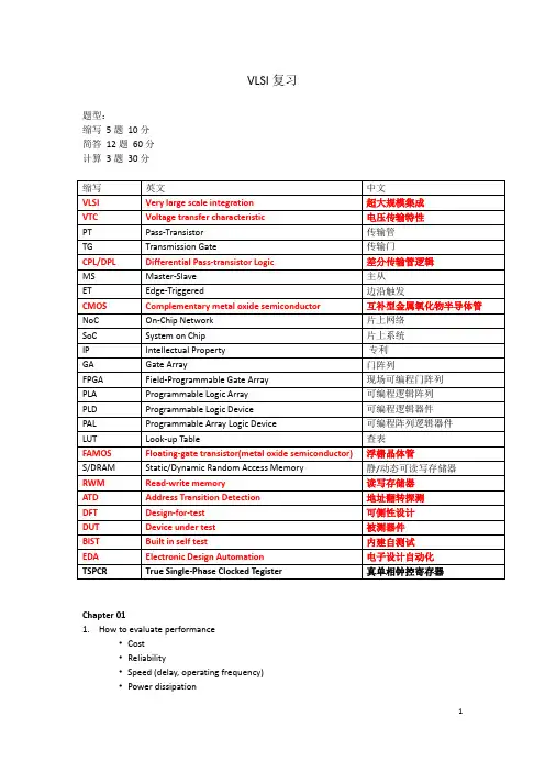
武汉理工大学《超大规模集成电路设计》考试习题及答案
- 格式:pdf
- 大小:411.25 KB
- 文档页数:10

招聘集成电路设计岗位笔试题与参考答案(某大型集团公司)(答案在后面)一、单项选择题(本大题有10小题,每小题2分,共20分)1、在集成电路设计中,以下哪种类型的设计通常负责处理数字逻辑功能?A、模拟集成电路B、数字集成电路C、混合信号集成电路D、射频集成电路2、以下哪种技术用于在集成电路设计中实现晶体管间的连接?A、光刻技术B、蚀刻技术C、键合技术D、离子注入技术3、在CMOS工艺中,P型MOSFET的阈值电压通常会随着温度的升高而:A. 增加B. 减少C. 不变D. 先增加后减少4、下列哪一项不是减少互连延迟的有效方法?A. 使用更细的金属线B. 使用更高介电常数的绝缘材料C. 减少金属层之间的距离D. 使用铜代替铝作为互连线材料5、集成电路设计中,以下哪种工艺主要用于制造CMOS(互补金属氧化物半导体)逻辑电路?A. 双极型工艺B. 金属氧化物半导体工艺C. 双极型/金属氧化物半导体混合工艺D. 双极型/CMOS混合工艺6、在集成电路设计中,以下哪个参数通常用来描述晶体管的开关速度?A. 饱和电压B. 输入阻抗C. 开关时间D. 集成度7、在集成电路设计中,用于描述电路逻辑功能的硬件描述语言不包括以下哪一种?A. VerilogB. VHDLC. C++D. SystemVerilog8、下列选项中,哪一个不是ASIC(专用集成电路)设计流程中的一个阶段?A. 逻辑综合B. 布局布线C. 系统集成D. 物理验证9、以下哪种工艺技术通常用于制造高性能的集成电路?A. 混合信号工艺B. CMOS工艺C. GaN(氮化镓)工艺D. BiCMOS工艺二、多项选择题(本大题有10小题,每小题4分,共40分)1、在CMOS工艺中,关于阱(well)的概念,下列说法正确的有:A. NMOS晶体管通常位于P型阱中B. PMOS晶体管通常位于N型阱中C. N阱用于隔离不同区域的晶体管,防止电流泄露D. P阱可以与N阱共存于同一层硅片上而不会相互影响2、关于集成电路版图设计中的DRC(Design Rule Check)规则,下列哪些陈述是正确的?A. DRC规则是为了确保电路性能优化B. DRC规则定义了最小特征尺寸、最小间距等制造限制C. 违反DRC规则可能会导致制造缺陷,如短路或开路D. DRC规则在所有半导体制造工艺中都是相同的3、关于集成电路设计,以下哪些是典型的电路设计类型?()A、模拟电路设计B、数字电路设计C、混合信号电路设计D、射频电路设计E、光电子电路设计4、在集成电路设计中,以下哪些因素会影响电路的功耗?()A、晶体管的工作状态B、电源电压C、电路的复杂度D、芯片的温度E、外部负载5、在集成电路设计过程中,下列哪些技术用于提高电路的性能?A. 使用更先进的制程技术B. 优化电路布局减少信号延迟C. 增加电源电压以提升速度D. 减少电路层数降低制造成本E. 应用低功耗设计方法6、下列哪些是实现CMOS逻辑门时需要考虑的关键因素?A. 输入电平的阈值B. 输出驱动能力C. 功率消耗D. 静态电流消耗E. 电路的工作频率7、以下哪些技术或方法属于集成电路设计中的模拟设计领域?()A. 信号处理算法B. 逻辑门电路设计C. 模拟电路仿真D. 功耗分析E. 版图设计8、在集成电路设计中,以下哪些步骤是进行版图设计的必要阶段?()A. 电路原理图设计B. 布局规划C. 逻辑分割D. 布局布线E. 版图检查9、在CMOS工艺中,影响MOSFET阈值电压的因素有哪些?A. 氧化层厚度B. 衬底掺杂浓度C. 栅极材料类型D. 源漏区掺杂浓度E. 温度F. 器件尺寸三、判断题(本大题有10小题,每小题2分,共20分)1、集成电路设计岗位的工程师需要具备扎实的数学基础和电子工程知识。
VLSI复习题型:缩写5题10分简答12题60分计算3题30分Chapter 011.How to evaluate performance•Cost•Reliability•Speed (delay, operating frequency)•Power dissipation2.Regenerative property3.Delay :Chapter 021.Inverter layout2.Photolithography process1)Oxidation layering(氧化层)2)Pthotoresist coating(涂光刻胶)3)Stepper exposure(光刻机曝光)4)Photoresist development and bake(光刻胶的显影和烘干)5)Acid etching(酸刻蚀)6)Spin, rinse, and dry(旋转,清洗和干燥)7)Various process steps:Ion implantation(离子注入)Plasma etching(等离子刻蚀)Metal deposition(金属沉淀)8)Photoresist removal( or ashing) 去除光刻胶(即“沙洗”)Chapter 031.Linear/ Saturation mode2.Long channel vs short channel3.Capacitances= structure capacitances+channel capacitances+MOS diffusion capacitances4.Resistance=MOS sructure resistance+source and drain resistance+cantact resistance+wiringresistanceWith silicidation R方块ˆ is reduced to the range 1 to 4 Ω/方块(source and drain resistance)Chapter 041.C wire = C pp + C fringe + C interwire2.Dealing with resistance:1)Use better interconnect materials2)More interconnect layers3.RC Mode•Lumped RC model–total wire resistance is lumped into a single R and total capacitance into a single C–good for short wires; pessimistic and inaccurate for long wires•Distributed RC model–circuit parasitics are distributed along the length, L, of the wire4.DelayDelay of a wire is a quadratic function of its length, LThe delay is 1/2 of that predicted (by the lumped model)5.Reflection coefficient【画传输图(or 波形),计算题】Chapter 051.V M∝(W/L)p/(W/L)nIncreasing the width of the PMOS moves V M towards V DD,‰Increasing the width of theNMOS moves V M towards GND.2.Delay3.Power in CMOS1.Dynamic power consumption: charging and discharging capacitors;Not a function of transistor sizes;Need to reduce C L,Vdd,and f to reduce power.2.Short circuit currents: short circuit path supply rails during switching;Keep the input and output rise/fall times the same;If Vdd<Vtn+|Vtp|,then short-circuit power can be eliminated.3.Leakage: leaking diodes and transistors4.Technology scaling modelsFull scalingFixed voltage scalingGeneral scalingChapter 061.Static CMOS- output connected to either Vdd or GND via a low-resistance path⏹High noise margins⏹Low output impedance, high input impedance⏹No steady state path between Vdd and GND⏹Delay is a function of load capacitance and transistor resistanceDynamic CMOS--relies on temporary storage of signal values on capacitance of high-impedance circuit nodes.⏹Simpler, faster gates⏹Increased sensitivity to noise2.Static vs dynamic circuit⏹In static circuit at every point in time (except when switching) the output is connectedto either GND or V DD via a low resistance path.--fan-in of N requires 2N devices⏹Dynamic circuits rely on the temporary storage of signal values on the capacitance ofhigh impedance nodes--requires only N+2 transistors--takes a sequence of precharge and conditional evaluation phases to realize logicfunctions.●conditions on output1) once the optput of a dynamic gate is discharged, it cannot be charged again until thenext precharge opreation.2) Inputs to the gate can make at most one transition during evaluation.3) Output can be in the high impedance state during and after evaluation(PDN off), stateis stored in C L.●Properties of Dynamic Gates1)Logic function is implemented by the PDN only–number of transistors is N + 2 (versus 2N for static complementary CMOS)–should be smaller in area than static complementary CMOS2)Full swing outputs (VOL = GND and VOH = VDD)3)Nonratioed--sizing of the devices is not important for proper functioning (only for performance)4) Faster switching speeds5) Power dissipation should be better- consumes only dynamic power –no short circuit power consumption since the pull- up path is not on when evaluating-lower C L--both C int(since there are fewer transistors connected to the drain outpu t) and C ext(since there the output load is one per connectedgate, not two) -by construction can have at most one transition per cycle – no glitching6) Needs a percharge clockbinational vs Sequential logic4.Why PMOS in PUN and NMOS in PDN?Threshold drops5.Ratioed logic: Pseudo-NMOS→Small area and load, but static power dissipationChapter 07tch vs Register⏹Latch: level sensitive----As for positive: passes inputs to Q when the clock is high----transparent mode;When clock is low----hold mode⏹Flip-flop: edge sensitive2.Bistable circuit:The cross coupling of two inverters results in a bistablecircuit (a circuit with two stable states)⏹Have to be able to change the stored value by making A (or B) temporarily unstable byincreasing the loop gain to a value larger than 1Done by applying a trigger pulse at Vi1 or Vi2the width of the trigger pulse need be only a little larger than the total propagation delayaround the loop circuit (twice the delay of an inverter)⏹Two approaches used1.cutting the feedback loop (mux based latch)2.overpowering the feedback loop (as used in SRAMs)3.MS ET timing properties⏹Set-up time: time before rising edge of clk that D must be valid⏹Propagation delay: time for QM to reach Q⏹Hold time: time D must be stable after rising edge of clk4.Pipelining5.Schmitt Trigger(rise—P; fall—N)Chapter 091.Cross Talk: An unwanted coupling from a neighboring signal wire to a network nodeintroduces an interference that is generally called cross talk.2.Dealing with Capacitive Cross Talk•Avoid floating nodes•Protect sensitive nodes•Make rise and fall times as large as possible•Differential signaling•Do not run wires together for a long distance•Use shielding wires•Use shielding layers3.Cross Talk and Performance: when neighboring lines switch in opposite direction of victimline, delay increases.4.Impact of resistance is commonly seen in power supply distribution:–IR drop–Voltage variationsChapter 101.Clock Nonidealities:⏹Clock skew: Spatial variation in temporally equivalent clock edges;⏹Clock jitter: Temporal variations in consecutive edges of the clock signal⏹Variation of the pulse width2.Clock Uncertainties----Source of clock uncertainty(图形填空)(重点)简答题:•Clock‐Signal Generation (1)•Manufacturing Device Variations (2)•Interconnect Variations (3)•Environmental Variations (4 and 5)•Capacitive Coupling (6 and 7)3.Impact of Positive/Negative Clock Skew and Clock jitter (重点)1.Positive clock skew:Clock and data flow in the same direction2.Negative clock skew: Clock and data flow in opposite directions3.Jitter cause T to vary on a cycle-by-cycle basisCombined impact of skew and jitter:Constraints on the minimum clock period (positive)4.To reduce dynamic power, the clock network must support clock gating (shutting down(disabling the clock ) units)5. Clock distribution techniques--Balanced paths(H-tree network, matched RC trees)--Clock grids: minimize absolute delay6.Matched RC trees, represents a floor plan that distributes the clock signal so that the interconnections carrying the clock signals to the functional subblocks are of equal length.7. 彩图9:The unbalanced load creates a large skew, by careful tuning of the wire width, the load is balanced, minimizing the skew.8. Dealing with Clock Skew and Jitter•To minimize skew, balance clock paths using H-treeor matched-tree clock distribution structures. •If possible, route data and clock in opposite directions;eliminates races at the cost of performance.•The use of gated clocks to help with dynamic power consumption make jitter worse.•Shield clock wires (route power lines –VDD or GND –next to clock lines) to minimize/eliminate coupling with neighboring signal nets.•Use dummy fills to reduce skew by reducing variations in interconnect capacitances dueto interlayer dielectric thickness variations.•Beware of temperature and supply rail variations and their effects on skew and jitter. •Power supply noise fundamentally limits the performance of clock networks.Chapter 111.Full adder(P=A+B)2.Static vs dynamic Manchester Carry ChainStatic dynamic3.Square Root Carry Select Adder (PPT 24)4.Wallace‐Tree Multiplier(PPT 32)5.Logarithmic ShifterChapter 121.Semiconductor Memory Classification2.Bit line & word line3.Memory Timing(DRAM vs SRAM)DRAM: Multiplexde AddressingSRAM: Self-timed Address Switching/Changing 4.MOS OR ROM5. SRAM vs DRAM6. DRAM Timing7. SRAM ATD(Address Transition Detection)Chapter 131.Two Important Test Properties•Controllability ‐measures the ease of bringing anode to a given condition using only the input pins•Observability ‐measures the ease of observing thevalue of a node at the output pins2.Test Approaches•Ad‐hoc testing•Scan based test•Self test3.Scan Register11。
招聘集成电路设计岗位笔试题与参考答案(某大型集团公司)(答案在后面)一、单项选择题(本大题有10小题,每小题2分,共20分)1.题目:集成电路设计中,以下哪个因素对电路性能影响最大?A. 晶圆尺寸B. 芯片制造工艺C. 电路架构设计D. 印刷电路板布局2.题目:在CMOS工艺中,以下哪种器件用于实现电流放大功能?A. PMOSB. NMOSC. 二极管D. 反相器3.在集成电路设计中,以下哪个因素对电路性能的影响最大?A. 电源电压B. 地线宽度C. 电路布局D. 输入输出信号4.集成电路的晶体管数量与其性能的关系,以下哪个说法是正确的?A. 晶体管数量越多,性能越好B. 晶体管数量越多,性能越差C. 晶体管数量适中,性能最佳D. 晶体管数量与性能无关5.在集成电路设计中,哪个过程是为了验证设计的正确性?A. 电路设计B. 制程模拟C. 芯片测试D. 设计验证6.在集成电路设计中,以下哪个因素是影响功耗的主要因素?A. 芯片尺寸大小B. 工作频率高低C. 电路设计复杂度D. 环境温度高低7、在集成电路设计中,以下哪种技术常用于降低功耗?()A. 增加时钟频率B. 优化布线结构C. 增加晶体管数量D. 优化算法设计以减少运算次数8、关于数字集成电路的下列说法中,哪项是不正确的?()A. 数字集成电路通过逻辑门电路实现数字信号的传输和处理。
B. 数字集成电路只能处理二进制信号。
C. 数字集成电路的设计和制造都需要先进的工艺和严格的标准。
D. 数字集成电路不适用于大规模生产,因为生产成本较高。
9.在集成电路设计中,以下哪个工具常用于逻辑综合?A. CAD工具B. 仿真器C. 物理验证工具D. 编程语言编译器 10. 集成电路设计中的时钟树结构有何作用?A. 减少布线资源B. 优化布线路径C. 提高电路性能D. 增加电路功耗二、多项选择题(本大题有10小题,每小题4分,共40分)1.关于集成电路设计流程,下列说法正确的是:A. 集成电路设计首要步骤是电路原理图设计。
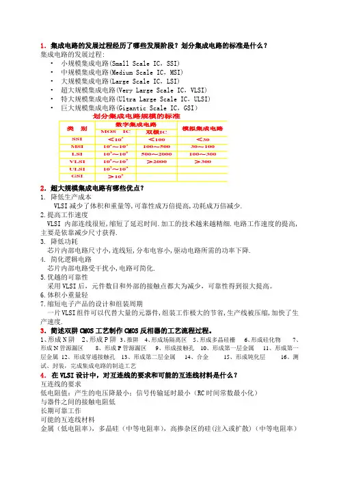
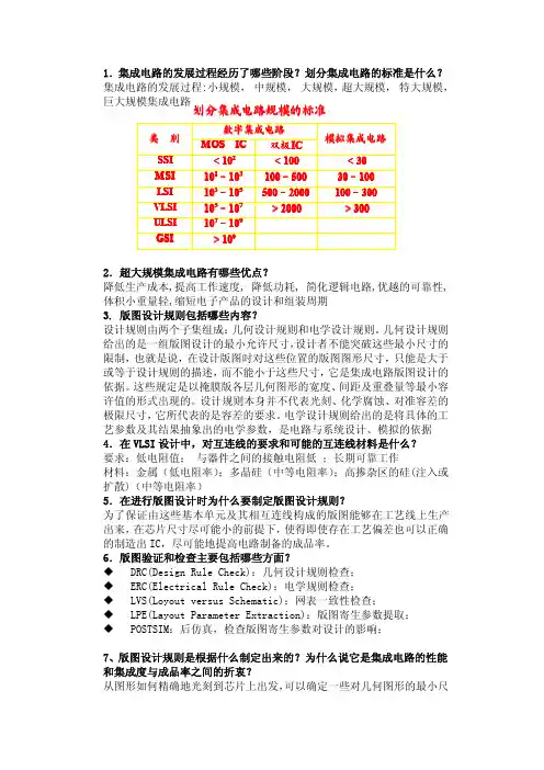
1.集成电路的发展过程经历了哪些发展阶段?划分集成电路的标准是什么?集成电路的发展过程:•小规模集成电路(Small Scale IC,SSI)•中规模集成电路(Medium Scale IC,MSI)•大规模集成电路(Large Scale IC,LSI)•超大规模集成电路(Very Large Scale IC,VLSI)•特大规模集成电路(Ultra Large Scale IC,ULSI)•巨大规模集成电路(Gigantic Scale IC,GSI)划分集成电路规模的标准2.超大规模集成电路有哪些优点?1. 降低生产成本VLSI减少了体积和重量等,可靠性成万倍提高,功耗成万倍减少.2.提高工作速度VLSI内部连线很短,缩短了延迟时间.加工的技术越来越精细.电路工作速度的提高,主要是依靠减少尺寸获得.3. 降低功耗芯片内部电路尺寸小,连线短,分布电容小,驱动电路所需的功率下降.4. 简化逻辑电路芯片内部电路受干扰小,电路可简化.5.优越的可靠性采用VLSI后,元件数目和外部的接触点都大为减少,可靠性得到很大提高。
6.体积小重量轻7.缩短电子产品的设计和组装周期一片VLSI组件可以代替大量的元器件,组装工作极大的节省,生产线被压缩,加快了生产速度.3.简述双阱CMOS工艺制作CMOS反相器的工艺流程过程。
1、形成N阱2、形成P阱3、推阱4、形成场隔离区5、形成多晶硅栅6、形成硅化物7、形成N管源漏区8、形成P管源漏区9、形成接触孔10、形成第一层金属11、形成第一层金属12、形成穿通接触孔13、形成第二层金属14、合金15、形成钝化层16、测试、封装,完成集成电路的制造工艺4.在VLSI设计中,对互连线的要求和可能的互连线材料是什么?互连线的要求低电阻值:产生的电压降最小;信号传输延时最小(RC时间常数最小化)与器件之间的接触电阻低长期可靠工作可能的互连线材料金属(低电阻率),多晶硅(中等电阻率),高掺杂区的硅(注入或扩散)(中等电阻率)5.在进行版图设计时为什么要制定版图设计规则?—片集成电路上有成千上万个晶体管和电阻等元件以及大量的连线。
大规模集成电路试卷2004A武汉大学东湖分校2005-2006学年第二学期期末考试试卷(A卷)试卷类型:开卷年级2004级专业计算机科学科目大规模集成电路姓名学号主考教师肖忠付分数一填空题(30分,每小题3分)1、 CPLD是指,FPGA是指。
2、综合是把层次中的一种表示转化成另一种表示的过程。
3、 EDA设计的输入方式有、和方式。
4、 STD_LOGIC数据类型定义了九种类型。
5、关系操作的结果为类型。
6、如果进程中不包含敏感信号表,那么在进程语句中必须包含。
7、signal a : in std_logic_vector ( 0 to 7 );………for I in a’range loop………for 语句的循环次数为次。
8、端口模式有。
仅供学习与交流,如有侵权请联系网站删除谢谢259、数据对象有三类。
10、一个N输入的查找表,需要SRAM存储N个输入构成的,需要占用个SRAM单元。
二简答题(50分,每小题10分)1、LUT的概念及举例说明一个四输入函数的LUT实现过程。
2、说明信号和变量的功能特点,以及在应用上有何不同?3、逻辑阵列块LAB包括哪几个部分?4、可编程逻辑器件有哪几种?各有什么特点?5、详细说明利用MAX+plus II 进行EDA设计的基本过程?三比较下面两个程序,说明两者的区别,并画出每个程序所描述的简单原理图。
(20分)1、 library IEEE;use IEEE.STD_LOGIC_1164.ALL;entity exp1 isPort ( clk,d1 : in std_logic;q1 : out std_logic);end exp1;architecture Behavioral of exp1 isbeginprocess(clk)variable a,b:std_logic;beginif clk'event and clk='1' then仅供学习与交流,如有侵权请联系网站删除谢谢25a:=d1;b:=a;q1<=b;end if;end process;end Behavioral;2、 library IEEE;use IEEE.STD_LOGIC_1164.ALL;entity exp2 isPort ( clk,d1 : in std_logic;q1 : out std_logic);end exp2;architecture Behavioral of exp2 issignal a,b:std_logic;beginprocess(clk)beginif clk'event and clk='1' thena<=d1;b<=a;q1<=b;end if;end process;end Behavioral;武汉大学计算机学院本科2006~2007学年第二学期考试试卷(A卷)课程名称:大规模集成电路(限120分钟)专业:本科姓名:学号:考分:说明:⒈答题书写在专用答题纸上,其他任何答题无效。
1、MOS集成电路的加工包括哪些基本工艺?各有哪些方法和工序?答:(1)热氧化工艺:包括干氧化法和湿氧化法;(2)扩散工艺:包括扩散法和离子注入法;(3)淀积工艺:化学淀积方法:1 外延生长法;2 热CVD法;3 等离子CVD 法;物理淀积方法:1 溅射法;2 真空蒸发法(4)光刻工艺:工序包括:1 涂光刻胶;2 预烘干;3 掩膜对准;4 曝光;5 显影;6 后烘干;7 腐蚀;8 去胶。
2、简述光刻工艺过程及作用。
答:(1)涂光刻胶:为了增加光刻胶和硅片之间的粘附性,防止显影时光刻胶的脱落,以及防止湿法腐蚀产生侧向腐蚀;(2)预烘干:以便除去光刻胶中的溶剂;(3)掩膜对准:以保证掩模板上的图形与硅片上已加工的各层图形套准;(4)曝光:使光刻胶获得与掩模图形相同的感光图片;(5)显影:将曝光后的硅片浸泡在显影液中,使正光刻胶的曝光部分和负光刻胶的未曝光部分被溶解掉;(6)后烘干:使残留在光刻胶中的有机溶剂完全挥发掉,提高光刻胶和硅片的粘接性及光刻胶的耐腐蚀性;(7)腐蚀:以复制在光刻胶上图形作为掩膜,对下层材料进行腐蚀,将图形复制到下层材料中;(8)去胶:除去光刻胶。
3、说明MOS晶体管的工作原理答:MOS晶体管有四种工作状态:(1)截止状态:即源漏之间不加电压时,沟道各电场强度相等,沟道厚度均匀,S、D之间没有电流I ds=0;(2)线性工作状态:漏源之间加电压Vds时,漏端接正,源端接负,沟道厚度不再均匀,在D端电位升为V d,栅漏极电位差为Vgs-Vtn,电场强度变弱,反型层变薄,并在沟道上产生由D到S的电场E ds,使得多数载流子由S端流向D端形成电流I ds,它与V ds变化呈线性关系:I ds=βn[(V gs-V tn)-V ds/2]V ds(3)饱和工作状态:Vs继续增大到V gs-V tn时,D端栅极与衬底不足以形成反型层,出现沟道夹断,电子运动到夹断点V gs-V ds=V tn时,便进入耗尽区,在漂移作用下,电子被漏极高电位吸引过去,便形成饱和电流,沟道夹断后,(V gs-V tn)不变,I ds 也不变,即MOS工作进入饱和状态,I ds=V gs-V tn/R c(4)击穿状态:当Vds增加到一定极限时,由于电压过高,晶体管D端得PN结发生雪崩击穿,电流急剧增加,晶体管不能正常工作。
招聘集成电路设计岗位笔试题与参考答案(某大型国企)(答案在后面)一、单项选择题(本大题有10小题,每小题2分,共20分)1、集成电路设计中,关于CMOS反相器的描述,以下哪项是正确的?A. CMOS反相器具有低功耗特性,但速度较慢。
B. CMOS反相器具有高速度特性,但功耗较高。
C. CMOS反相器具有低功耗特性,且速度较快。
D. CMOS反相器具有高速度特性,但功耗较低。
2、在集成电路设计中,以下哪个因素对电路的性能有重要影响?A. 晶圆尺寸B. 制造工艺C. 电路规模D. 所有上述因素3、在集成电路设计中,以下哪个因素对电路性能的影响最大?A. 电源电压B. 地线宽度C. 电阻值D. 电容值4、在CMOS工艺中,以下哪种器件主要用于实现电流放大功能?B. NMOSC. 二极管D. 反相器5、(关于集成电路设计基础)以下关于集成电路设计的描述中,哪项是正确的?A. 集成电路设计完全依赖于自动化工具,无需人工干预。
B. 集成电路设计过程中,版图设计是第一步。
C. 集成电路设计主要关注电路的功能实现,而不考虑其物理实现。
D. 在集成电路设计中,功耗和性能同样重要,需要平衡考虑。
6、(关于数字集成电路设计)在数字集成电路设计中,关于时序分析,以下说法错误的是?A. 时序分析是确保电路在规定的时钟周期内正确工作的关键步骤。
B. 时序分析只关注组合逻辑部分,不涉及时序逻辑部分。
C. 时序分析包括建立时序和保持时序的分析。
D. 时序分析是确保芯片性能的重要手段之一。
7、在集成电路设计中,以下哪个因素对电路性能的影响最大?A. 电源电压B. 地址线宽度C. 数据总线宽度D. 输入输出接口8、在CMOS工艺中,以下哪个器件用于实现电流隔离?A. 晶体管C. 互斥开关D. 绝缘层9、下列哪个选项是集成电路设计中常用的EDA工具软件?A. AutoCADB. SolidWorksC. Altium DesignerD. MATLAB 10、在集成电路设计中,关于CMOS工艺的特点描述正确的是?A. CMOS工艺只能用于数字电路的设计B. CMOS工艺功耗大,不适合低功耗应用C. CMOS工艺可以同时实现数字与模拟电路的设计D. CMOS工艺不兼容其他集成工艺类型二、多项选择题(本大题有10小题,每小题4分,共40分)1、关于集成电路设计的基础知识中,下列哪些说法是正确的?()选项:A. 集成电路设计主要涉及到模拟电路、数字电路和混合信号电路设计。
2024年招聘集成电路设计岗位笔试题及解答(某世界500强集团)(答案在后面)一、单项选择题(本大题有10小题,每小题2分,共20分)1、下列晶体管类型的半导体材料中,通常用于集成电路制造中的集电极,其来源最为广泛且成本较低的是?A. 氮化镓 (GaN)B. 硅 (Si)C. 锗 (Ge)D. 金刚石2、在集成电路设计行业中,总线宽度是指一次可以传输的信号数量。
下列总线的有效性排列中,哪一组是可以用在8位处理器的?A. 1位或4位总线B. 4位或8位总线C. 8位或16位总线D. 4位或16位总线3、下列哪种电路拓扑结构通常用于实现高增益放大器?A.மமமமமமமமமமB. 喜欢的肯定是什么?4、CMOS工艺中,为降低漏电流和提高开关速度,通常采用什么措施?A. 增加阈值电压B. 减少阈值电压C. 降低工作电压D. 提高工作电压5.在集成电路设计中,以下哪个因素对芯片的性能有最大影响?A. 电流大小B. 电压水平C. 晶体管尺寸D. 电阻值6.在设计集成电路时,以下哪种布局方法可以最小化信号传输延迟?A. 混合布局B. 紧凑布局C. 顺序布局D. 扇形布局7、数字选数字。
在模拟到数字转换电路中,使用最多的技术是()。
A、反相放大器B、运算放大器C、二极管放大器D、集成运放放大器8、数字选数字。
双极型晶体管在半导体工艺中,通常使用()掺杂技术。
A、P区掺杂B、N区掺杂C、平面掺杂D、表面掺杂9、设一款MMIC Amplifier电路的截止频率为10GHz,其放大倍数为20dB,则该放大器在1kHz处的增益 (以分贝为单位)A.约为20dBB.约为1.2dBC.约为0dBD.约为200dB 10、下列哪种晶体管的工作原理是基于电流的控制效果?A.MOSFETB.BJTTFETD.FinFET二、多项选择题(本大题有10小题,每小题4分,共40分)1.集成电路设计中,以下哪个因素对芯片性能影响最大?A. 电流大小B. 电压频率C. 电磁干扰D. 噪声大小2.在CMOS工艺中,以下哪种器件主要用于实现逻辑非功能?A. 二极管B. 晶体管C. 互连D. 电容3、集成电路设计中,每种不同类型的门电路都有其组成形式和特性方程,其中三态门(Out,tree)电路的特性方程,下述的英文表达准确的为:() A) Out = (A!) B) Out = ( *mc*ai) C) Out = ( ) is not the right choice D)Out = 0并且向上false4、某一电路的表达式为 Out = ( * ),( ) 表示废物符号,关于此电路的描述正确的是哪些?( ) A)只要有一个输入为1,则 Out=1,其 Low电平比单输出 t 高B)当 A,B,C 三个输入都为 0 时, Out=0 C)若 C=0,无论输入为0,1均不产生 anything D)三种输入相等时,三种条件下的结果一样5、下列关于 CMOS 集成电路的描述,哪些是正确的?( )A. CMOS 电路采用互补型 MOSFET 作为开关元件B. CMOS 电路在高速工作时功耗较低C. CMOS 电路主要用于模拟信号处理D. CMOS 电路在静态功耗方面较低6、下列关于设计流程中布局規劃的描述,哪些是正确的?( )A. 布局规划直接影响到芯片的性能B. 布局规划需要考虑每一级线路的容量C. 布局规划主要关心电路的功能实现D. 布局规划阶段可以随意修改电路结构7、在数字电路设计中,以下哪些电压类型是常见的逻辑门电压()。
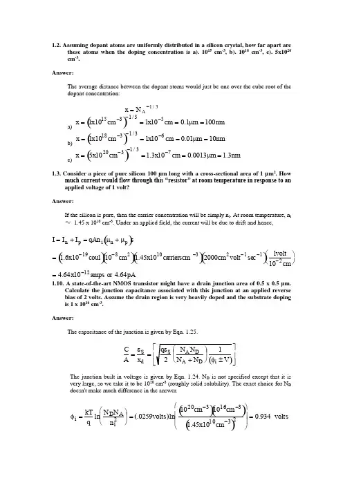
1.2. Assuming dopant atoms are uniformly distributed in a silicon crystal, how far apart arethese atoms when the doping concentration is a). 1015 cm -3, b). 1018 cm -3, c). 5x1020 cm -3.Answer:The average distance between the dopant atoms would just be one over the cube root of the dopant concentration:x =N A -1/3a)x =1x1015cm-3()-1/3=1x10-5cm =0.1μm =100nm b)x =1x1018cm-3()-1/3=1x10-6cm =0.01μm =10nmc)x =5x1020cm-3()-1/3=1.3x10-7cm =0.0013μm =1.3nm1.3. Consider a piece of pure silicon 100 µm long with a cross-sectional area of 1 µm2. Howmuch current would flow through this “resistor” at room temperature in response to an applied voltage of 1 volt?Answer: If the silicon is pure, then the carrier concentration will be simply n i . At room temperature, n i≈ 1.45 x 1010 cm -3. Under an applied field, the current will be due to drift and hence,I =I n +I p =qAn i μn +μp ()ε=1.6x10⁻¹⁹coul ()10-8cm2()1.45x10¹⁰carrierscm-3()2000cm 2volt-1sec-1()1volt 10-2cm ⎛ ⎝ ⎫⎭=4.64x10⁻¹²amps or 4.64pA1.10. A state-of-the-art NMOS transistor might have a drain junction area of 0.5 x 0.5 µm.Calculate the junction capacitance associated with this junction at an applied reverse bias of 2 volts. Assume the drain region is very heavily doped and the substrate doping is 1 x 1016 cm -3. Answer:The capacitance of the junction is given by Eqn. 1.25.C A =εS x d =q εS 2N A ND N A +N D ⎛ ⎝ ⎫ ⎭ ⎪ 1φi ±V ()⎡ ⎣ ⎢⎤ ⎦ ⎥The junction built-in voltage is given by Eqn. 1.24. N D is not specified except that it is very large, so we take it to be 1020 cm -3 (roughly solid solubility). The exact choice for N D doesn't make much difference in the answer.φi =kT q ln N D N An i 2⎛ ⎝ ⎫ ⎭⎪ =.0259volts ()ln 1020cm -3()1016cm -3()1.45x1010cm-3()2⎛ ⎝ ⎫⎭⎪ ⎪ =0.934 voltsSince N D >> N A in this structure, the capacitance expression simplifies toC A ≅εSW=qεS2N A()1φi±V()⎡⎣⎢⎤⎦⎥=1.6x10⁻¹⁹coul()11.7()1016cm-3()8.86x10⁻¹⁴Fcm-1()2()2.934volts()⎡⎣⎢⎤⎦⎥ =1.68x10⁻⁸Fcm-2Given the area of the junction (0.25 x 10⁻⁸ cm2, the junction capacitance is thus 4.2 x 10⁻¹⁷ Farads.3.2. A boron-doped crystal pulled by the Czochralski technique is required to have aresistivity of 10 Ω cm when half the crystal is grown. Assuming that a 100 gm pure silicon charge is used, how much 0.01 Ω cm boron doped silicon must be added to the melt? For this crystal, plot resistivity as a function of the fraction of the melt solidified. Assume k 0 = 0.8 and the hole mobility µp = 550 cm 2 volt -1 sec -1.Answer:Using the mobility value given, and ρ=1q μN A we have:10 Ω cm ⇒ N A = 1.14 x 1015 cm -3 and 0.01 Ω cm ⇒ N A = 1.14 x 1018 cm -3From Eqn. 3.38, C S =C O k O 1-f ()k O -1and we want C S = 1.14 x 1015 cm -3 when f =0.5. Thus, solving for C 0 the initial doping concentration in the melt, we have:C 0=1.14x10150.81-0.5()0.2=1.24x1015cm -3But C 0=I 0V 0=# of impurities unit vol of me lt =(Doping)(Vol. of 0.01 Ωcm)Vol 100 gm Si∴ Wgt added of 0.01 Ω c m Si = C 0Doping ⎛ ⎝ ⎫⎭ 100gm ()=0.109gmThe resistivity as a function of distance is plotted below and is given byρx ()=1q μN A x ()=1-f ()1-k 0q μC 0k 0=11.5Ωcm 1-f ()0.2024681012R e s i s t i v i t y0.20.40.60.81Fraction S olidified - f3.3. A Czochralski crystal is pulled from a melt containing 1015 cm -3 boron and 2x1014 cm -3phosphorus. Initially the crystal will be P type but as it is pulled, more and more phosphorus will build up in the liquid because of segregation. At some point the crystal will become N type. Assuming k O = 0.32 for phosphorus and 0.8 for boron, calculate the distance along the pulled crystal at which the transition from P to N type takes place.Answer:We can calculate the point at which the crystal becomes N type from Eqn. 3.38 as follows:C S Phos ()=C 0k 01-f ()k 0-1=2x10¹⁴()0.32()1-f ()-0.68C S Boron ()=C 0k 01-f ()k 0-1=1015()0.8()1-f ()-0.2At the point where the cross-over occurs to N type, these two concentrations will be equal. Solving for f, we findf ≅0.995Thus only the last 0.5% of the crystal is N type.3.6. Suppose your company was in the business of producing silicon wafers for thesemiconductor industry by the CZ growth process. Suppose you had to produce the maximum number of wafers per boule that met a fairly tight resistivity specification. a). Would you prefer to grow N type or P type crystals? Why?b). What dopant would you use in growing N-type crystals? What dopant would you use in growing P type crystals? ExplainAnswer:a). Boron has the segregation coefficient closest to unity of all the dopants. Thus itproduces the most uniform doping along the length of a CZ crystal. Thus P type would be the natural choice.b). For P type, the obvious (and only real choice) is boron as explained in part a). For N type crystals Fig. 3-18 shows that either P or As would be a reasonable choice since their segregation coefficients are quite close and are better than Sb. Table 3-2 indicates that P might be slightly preferred over As because its k O value is slightly closer to 1.4.1. An IC manufacturing plant produces 1000 wafers per week. Assume that each wafer contains 100 die, each of which can be sold for $50 if it works. The yield on these chips is currently running at 50%. If the yield can be increased, the incremental income is almost pure profit because all 100 chips on each wafer are manufactured whether they work or not. How much would the yield have to be increased to produce an annual profit increase of $10,000,000?Answer:At 1000 wafers per week, the plant produces 52,000 wafers per year. If each wafer has 50 good die each of which sells for $50, the plant gross income is simplyIncome = (52,000)(50)($50) = $130,000,000 per year.To increase this income by $10,000,000 requires that the yield increase by10130≅7.7%4.3. As MOS devices are scaled to smaller dimensions, gate oxides must bereduced in thickness.a. As the gate oxide thickness decreases, do MOS devices become more or lesssensitive to sodium contamination? Explain.b. As the gate oxide thickness decreases, what must be done to the substrate doping (oralternatively the channel V TH implant, to maintain the same V TH? Explain.Answer:a). From the text, Na+ contamination causes threshold voltage instabilities in MOS devices.Also from Eqn. 4.1, the threshold voltage is given byV TH=V FB+2φf+2εS qN A2φf()C OX+qQ MC OXAs the gate oxide thickness decreases, C OX increases, so the same amount of mobile charge Q M will have less effect on V TH as oxides get thinner. Therefore MOS devices are less sensitive to sodium contamination.b). Using the same expression for V TH as in part a), we observe that as the oxide thickness decreases, (C OX increases), to maintain the same V TH, N A will have to increase. N A willactually have to increase by the square root of the oxide thickness decrease to keep V TH constant.4.4. A new cleaning procedure has been proposed which is based on H2O saturated with O2as an oxidant. This has been suggested as a replacement for the H2O2 oxidizing solution used in the RCA clean. Suppose a Si wafer, contaminated with trace amounts of Au, Fe and Cu is cleaned in the new H2O/O2solution. Will this clean the wafer effectively?Why or why not? Explain.Answer:As described in the text, cleaning metal ions off of silicon wafers involves the following chemistry:M↔M z++ze-The cleaning solution must be chosen so that the reaction is driven to the right because this puts the metal ions in solution where they can be rinsed off. Since driving the reaction to the right corresponds to oxidation, we need an oxidizing solution to clean the wafer.H2O/O2 is certainly an oxidizing solution. But whether it cleans effectively or not depends on the standard oxidation potential of the various possible reactions. From Table 4-3 in the text, we have:Oxidant/ Reductant Standard OxidationPotential (volts)Oxidation-Reduction ReactionSiO2/Si0.84Si+2H2O↔SiO2+4H++4e-Fe3+/Fe 0.17Fe↔Fe3++3e-Cu2+/Cu -0.34Cu↔Cu2++2e-O2/H2O-1.232H2O↔O2+4H++2e-Au3+/Au -1.42Au↔Au3++3e-The stronger reactions (dominating) are at the bottom.Thus the H2O/O2 reaction will clean Fe and Cu, but it will not clean Au off the wafer.4.5. Explain why it is important that the generation lifetime measurement illustrated inFigure 4-19 is done in the dark.Answer:The measurement depends on measuring carriers generated thermally in the silicon substrate (or at the surface). If light is shining on the sample, then absorbed photons can also generate the required carriers. As a result, the extracted generation lifetime with the light on would really be measuring the intensity of the incident light and not a basic property of the silicon material.5.1. Calculate and plot versus exposure wavelength the theoretical resolution and depth offocus for a projection exposure system with a NA of 0.6 (about the best that can be done today). Assume k 1 = 0.6 and k 2 = 0.5 (both typical values). Consider wavelengths between 100 nm and 1000 nm (DUV and visible light). ). Indicate the common exposure wavelengths being used or considered today on your plot (g-line, i-line, KrF and ArF). Will an ArF source be adequate for the 0.13 µm and 0.1 µm technology generations according to these simple calculations?Answer:The relevant equations are simply∴R =k 1 λNA =0.6λ0.6 a nd DOF =±k 2λNA ()2=±0.5λ0.6()2These equations are plotted below. Note that the ArF (193 nm) will not reach 0.13 µm or 0.1 µm resolution according to these simple calculations. In fact, with more sophisticated techniques such as phase shift masks, off axis illumination etc., ArF is expected to reach 0.13 µm and perhaps the 0.1 µm generations.00.20.40.60.811.21.4R e s o l u t i o n , D O F 祄20040060080010001200Exposure Wavelength nmRe solutionDepth ofFocusg-linei-line KrFArF5.3. An X-ray exposure system uses photons with an energy of 1 keV. If the separation between the mask and wafer is 20 µm, estimate the diffraction limited resolution that is achievable by this system.Answer:The equivalent wavelength of 1 keV x-rays is given byE =h ν=hc λ∴ λ=hc E=4.14x10⁻¹⁵eVsec ()3x1010cm sec -1()103eV=1.24x10⁻⁷cm =1.24 nmX-ray systems operate in the proximity printing mode, so that the theoretical resolution is given by Eqn. 5.12:Resolution =λg =1.24x10⁻³μm ()20μm ()=0.15μm5.8. As described in this chapter, there are no clear choices for lithography systems beyondoptical projection tools based on 193-nm ArF eximer lasers. One possibility is an optical projection system using a 157-nm F 2 excimer laser.a. Assuming a numerical aperture of 0.8 and k 1 = 0.75, what is the expected resolution of such a system using a first order estimate of resolution?b. Actual projections for such systems suggest that they might be capable of resolving features suitable for the 2009 0.07 µm generation. Suggest three approaches to actually achieving this resolution with these systems.Answera). The simple formula for resolution isR =k 1λNA =0.750.157μm0.8=0.147μmb). The calculated resolution in part a is a factor of two larger than required for the 0.07 µm generation. Therefore some “tricks” will have to be used to actually achieve such resolution. There are a number of possibilities:1. Use of phase-shift masks. This technique, discussed in this chapter, has the potential for significant resolution improvements. It works by designing a more sophisticated mask. Simple masks are digital - black or white. Phase shifting adds a second material to the mask features, usually at the edges which shifts the optical phase and sharpens up the aerial image. Sophisticated computer programs are required to design such masks.2. Use of optical proximity correction in the mask design. This is another approach to designing a better mask and as discussed in class, can also improve resolution significantly. The approach involves adding extra features to the mask, usually at corners where features are sharp, to compensate for the high frequency information lost to diffraction effects.3. Off-axis illumination. This allows the optical system to capture some of the higher order diffracted light and hence can improve resolution.5.9. Current optical projection lithography tools produce diffraction limited aerial images. A typical aerial image produced by such a system is shown in the simulation below where a square and rectangular mask regions produce the image shown. (The mask features are the black outlines, the calculated aerial image is the grayscale inside the black rectangles.) The major feature of the aerial image is its rounded corners compared to the sharp square corners of the desired pattern. Explain physically why these features look the way they do, using diffraction theory and the physical properties of modern projection optical lithography tools.Answer:Modern optical projection lithography systems are limited in the resolution they can achieve by diffraction effects. The finite size of the focusing lens means that the high order diffraction components are “lost” and are therefore not available to help in printing a replica of the mask image. But the high frequency spatial components are exactly the components that contain information about “sharp” features, i.e. corners etc. Thus the projected aerial image loses this information and corners become rounded. The only ways to improve the image are by using shorter wavelength light, or a higher NA lens.5.10. Future optical lithography systems will likely use shorter exposure wavelengths toachieve higher resolution and they will also likely use planarization techniques to provide “flat” substrates on which to expose the resist layers. Explain why “flat”substrates will be more important in the future than they have been in the past. Answer:As the wavelength of the exposure system decreases, the depth of focus of the exposure system also decreases. Thus it will be necessary to make sure that the resist in which the image is to be exposed, is flat and does not require much depth of focus. Planarization techniques will be required to accomplish this. This could mean CMP to planarize the substrate before the resist is applied, or it could mean using a spun on resist which planarizes the substrate and which is then covered with a thin, uniform imaging resist layer.6.4. Construct a HF CV plot for a P-type silicon sample, analogous to Fig. 6-9. Explain your plot based on the behavior of holes and electrons in thesemiconductor in a similar manner to the discussion in the text for Fig. 6.9.Answer:CCCa)b)c)C OC OC OC OC OC O C Dx D- V GV GV GV G+++---V TH Q G Q I Q DC DMinx DMax+ V Gh +P Silicon Doping = N A--------h +Electrons------------h +++V GThe C-V plot looks basically the same as the N substrate example in the text, that we discussed in class, except that the horizontal axis is flipped. For negative applied gate voltages, the majority carrier holes in the substrate are attracted to the surface. This is the accumulation region a) above. We measure just C OX for the capacitance since there is no depletion in the substrate. For + V G , the holes are driven away from the surface creating first a depletion region as in b) and finally an inversion layer of electrons as in c). Themeasured capacitance drops as we move into depletion and finally reaches a minimum value after an inversion layer forms.The C-V curves shown are high frequency curves. As discussed in the text, the capacitance remains at its minimum value for + V G values greater than V TH because the inversion layer electrons cannot be created or destroyed as fast as the signal is changing. Hence the small AC signal must “wiggle” the bottom of the depletion region to balance ∆V G.6.6. In a small MOS device, there may be a statistical variation in V T due to differences inQ F from one device to another. In a 0.13 µm technology minimum device (gate oxide area = 0.1µm x 0.1µm) with a 2.5nm gate oxide, what would the difference in threshold voltage be for devices with 0 or 1 fixed charge in the gate oxide?Answer:The oxide capacitance isC ox=εAd=3.9⨯8.854⨯10-14()0.1⨯10-4()0.1⨯10-4()2.5⨯10-7=1.38⨯10-16The change in threshold voltage is given by∆V T=qQ FC ox=1.6⨯10-19()1()1.38⨯10-16=1.1mVThis shows that a single electron trap in a gate oxide will have a negligible effect on thethreshold voltage at this technology generation.6.12 A silicon wafer is covered by an SiO2 film 0.3 μm thick.a. What is the time required to increase the thickness by 0.5 μm by oxidation in H2Oat 1200˚C?b. Repeat for oxidation in dry O2at 1200˚C.Answer:We will perform the calculation for <111> silicon wafers. For <100> wafers, the linear rate constant should be divided by 1.68.a. At 1200˚C, in H2OB=3.86⨯102exp-0.78 kT⎛ ⎝ ⎫⎭ =0.829μm2/hrB A =1.63⨯108exp-2.05kT⎛⎝⎫⎭ =15.86μm/hrA=0.052μmThe initial oxide, if grown at 1200˚C would have taken this long to growτ=x i2+Ax iB=0.3()2+0.052()0.3()0.829=0.127hrThe time required to grow 0.8μm at 1200˚C isτ=x i 2+Ax i B =0.8()2+0.052()0.8()0.829=0.822hrThus, the time required to add 0.5μm to an existing 0.3μm film is0.822-0.127=0.695hr or 41.7 minutes.b. At 1200˚C, in dry oxygenB =7.72⨯102exp - 1.23k(1200+273)⎛ ⎝ ⎫⎭ =0.048μm 2/hrB A =6.23⨯106exp -2.0kT ⎛ ⎝ ⎫⎭ =0.899μm /hrA =0.053μmThe initial oxide would have taken 2.206 hours to grow in dry oxygen, it would require 14.217 hours to grow 0.8μm , thus would require an additional 12 hours to add 0.5μm to an existing 0.3μm film.6.13. Suppose an oxidation process is used in which (100) wafers are oxidized in O 2 for threehrs. at 1100˚C, followed by two hrs. in H 2O at 900˚C, followed by two hrs in O 2 at 1200˚C. Use Figs. 6-19 and 6-20 in the text to estimate the resulting final oxide thickness. Explain how you use these figures to calculate the results of a multi-step oxidation like this.Answer:We can use these figures to estimate the oxide thickness as follows. First, we use Fig. 6-19 for the first dry oxidation cycleA three hour oxidation at 1100˚C produces an oxide thickness of about 0.21 µm. We nextuse Fig. 6-20 for the wet oxidation as shown below. The oxidation is 2 hrs in H 2O at 90 ˚C. We start by finding the point on the 900˚C curve that corr esponds to 0.21 µm since this is the starting oxide thickness. This is point A. We then move along the 900˚C curve by two hours to point B. This corresponds to a thickness of about 0.4 µm which is the thickness at the end of the wet oxidation.00.40.81.21.62Ox i d e T h i c k n e s s- m i c r o ns12345678Time - hours9101100 ÞC700 ÞC 1000 ÞC900 ÞC800 ÞCABWe now go back to Fig. 6-19 for the final dry O 2 cycle. This process is 2 hrs at 1200˚C. Westart by finding the point on the 1200˚C curve that corresponds to a starting oxide thickness of 0.4 µm. This is point A below. We then increment the time by 2 hrs along the 1200˚C curve, to arrive at a final oxide thickness of about 0.5 µm.6.18. Silicon on Insulator or SOI is a new substrate material that is being considered forfuture integrated circuits. The structure, shown below, consists of a thin single crystal silicon layer on an insulating (SiO 2) substrate. The silicon below the SiO 2 provides mechanical support for the structure. One of the reasons this type of material is being considered, is because junctions can be diffused completely through the thin silicon layer to the underlying SiO 2. This reduces junction capacitances and produces faster circuits. Isolation is also easy to achieve in this material, because the thin Si layer can be completely oxidized, resulting in devices completely surrounded by SiO 2. A LOCOS process is used to locally oxidize through the silicon as shown on the right below. Assuming the LOCOS oxidation is done in H 2O at 1000˚C, how long will it take to oxidize through the 0.3 µm silicon layer? Calculate a numerical answer using the Deal Grove model.Answer:To oxidize completely through a 0.3 µm silicon layer, we will need to grow (2.2)(0.3 µm) = 0.66 µm of SiO 2. At 1000˚C in H 2O, the Deal Grove rate constants are given by (Table 6-2):B =3.86x10²exp -0.78eV kT ⎛ ⎝ ⎫⎭ =0.316μm 2hr -1B A =1.63x1081.68exp -2.05eV kT ⎛ ⎝ ⎫ ⎭ =0.747μmhr -1∴t =0.66()20.316+0.660.747≅2.25 hours6.23. As part of an IC process flow, a CVD SiO 2 layer 1.0 µm thick is deposited on a <100>silicon substrate. This structure is then oxidized at 900˚C for 60 minutes in an H 2O ambient. What is the final SiO 2 thickness after this oxidation? Calculate an answer, do not use the oxidation charts in the text .Answer:At 900˚C in H 2O, the oxidation rate constants are given by:B =3.86x10²exp -0.788.62x10-5()1173()⎛ ⎝ ⎫ ⎭ ⎪ μm 2 hr -1=0.17 μm 2 hr -1B A =1.63x1081.68exp - 2.058.62x10-5()1173()⎛ ⎝ ⎫⎭ ⎪ μm hr -1=0.152 μm hr -1The initial oxide on the wafer is 1.0 µm thick. This corresponds to a τ ofτ=1()2+1()0.170.152⎛ ⎝⎫ ⎭0.17=12.46 hoursThus the final oxide thickness is given byx o =0.172()0.152()1+13.461.11()24()0.17()-1⎧ ⎨ ⎪ ⎩ ⎪ ⎫⎬ ⎪ ⎭ ⎪=1.064 μmThus not much additional oxide grows.Chapter 7 Problems7.1. A resistor for an analog integrated circuit is made using a layer of deposited polysilicon0.5 µm thick, as shown below.SiSiO 2Polysilicon(a) (a)The doping the polysilicon is 1⨯1016 cm -3. The carrier mobilityμ=100cm 2V -1se c -1 is low because of scattering at grain boundaries. If theresistor has L=100µm, W=10µm, what is its resistance in Ohms?(b) (b) A thermal oxidation is performed on the polysilicon for 2 hours at 900˚C in H 2O . Assuming B/A for polysilicon is 2/3 that of <111> silicon, what is thepolysilicon thickness that remains.(c) (c) Assuming that all of the dopant remains in the polysilicon (i.e. does notsegregate to oxide), what is the new value of the resistor in (a). Assume the mobility does not change.Answer:(a)ρ=1nq μ=11⨯1016()1.6⨯10-19()100()=6.25ΩcmρS =ρx j = 6.250.5⨯10-4=125k ΩR =10010ρS =1.25M Ω(10square s )(b ) The linear rate coefficient at 900˚C isB A ⎛ ⎝ ⎫ ⎭ poly =231.63⨯108exp -2.05kT ⎛ ⎝ ⎫ ⎭ ⎛ ⎝ ⎫ ⎭=0.170μm hr -1The parabolic rate constant for poly is unchanged:B poly =3.86⨯102exp -0.78kT ⎛ ⎝ ⎫⎭ =0.172μm 2hr -1A poly =1.01μm The oxide thickness isx o =A 21+tA 2/4B -1⎧ ⎨ ⎩ ⎫ ⎬⎭x o =1.0121+21.01()2/40.172()-1⎧ ⎨ ⎩ ⎫ ⎬ ⎭ =0.27μmThis oxide consumes a silicon thickness of 0.45*0.27=0.12 µm, leaving a remaining polysilicon thickness of 0.5-0.12=0.38 µm and contains all the dopant with a concentration of1⨯1016()0.50.38=1.31⨯1016cm-3(c) Since the concentration has gone up and the thickness has gone down by the same factor, the polysilicon restivity and hence the resistance of the line remains the same.7.4. Suppose we perform a solid solubility limited predeposition from a doped glass sourcewhich introduces a total of Q impurities / cm 2.(a) (a) If this predeposition was performed for a total of t minutes, how long would ittake (total time) to predeposit a total of 3Q impurities / cm 2 into a wafer if the predeposition temperature remained constant.(b) (b) Derive a simple expression for the Dt ()drive -in which would be required todrive the initial predeposition of Q impurities / cm 2 sufficiently deep so that the final surface concentration is equal to 1% of the solid solubility concentration. Thiscan be expressed in terms ofDt ()predep and the solid solubility concentrationC S .Answer:(a)Q =2C SπDt ⇒Q ∝t∴3Q ⇒9t(b)C 0,t ()drive -in =QπDt =0.01C SQ =2C SπDt ()predep∴2πDt ()predep Dt ()drive -in =0.01∴Dt ()drive -in =200π⎛ ⎝ ⎫ ⎭ 2Dt ()predep7.7. A boron diffusion is performed in silicon such that the maximum boron concentration is1 x 1018 cm -3. For what range of diffusion temperatures will electric field effects and concentration dependent diffusion coefficients be important?Answer:Electric field effects and concentration dependent diffusion are both important when the doping concentration exceeds the intrinsic electron (or hole) concentration. The intrinsic orbackground electron concentration is n i which increases with higher temperature. This provides a background sea of electrons or holes in the lattice at a given temperature. If the doping exceeds this concentration, then these extrinsic effects are important.When the temperature is below the temperature where n i =1⨯1018/cm 3, these effectswill become dominant since they often depend on n /n i (where n =N A or n =N D to a first approximation).n i =3.9⨯1016T 32exp -0.605kT ⎛ ⎝ ⎫⎭By trial and error, n i =1⨯1018/cm 3at T=720C.Therefore, extrinsic effects become important below 720˚C.7.15. A silicon wafer is uniformly doped with boron (2 x 1015 cm -3) and phosphorus (1 x 1015cm -3) so that it is net P type. This wafer is then thermally oxidized to grow about 1 µm of SiO 2. The oxide is then stripped and a measurement is made to determine the doping type of the wafer surface. Surprisingly it is found to be N type. Explain why the surface was converted from P to N type. Hint: Consider the segregation behavior of dopants when silicon is oxidized.Answer:The boron segregates preferentially into the growing oxide, thus depleting the surface concentration in the silicon. The phosphorus on the other hand preferentially segregates (piles-up) on the silicon side of the interface. Both of these effects act in the same direction and tend to make the surface of the silicon more N-type.It is for this reason that a P-type “channel stop” implant is almost always needed under a locally oxidized lightly doped P-type region, to prevent depletion of the P-type dopant in the substrate and in the worst case to prevent an N-type channel from forming. 7.20. Fig. 7.38 shows that a wet oxidation produces a significantly higher C I /C I *than doesa dry O 2 oxidation. Explain quantitatively why this should be the case. Answer:BecauseC I ∝dx dta faster oxidation rate produces a higher interstitial supersaturation. Thus, wet oxidationproduces a higher C I /C I * than dry oxidation, for the same time at the same temperature.Chapter 8 Problems8.1. Arsenic is implanted into a lightly doped p-type Si substrate at an energy of 75keV . Thedose is 1⨯1014/cm 2. The Si substrate is tilted 7˚ with respect to the ion beam to make it appear amorphous. The implanted region is assumed to be rapidly annealed so that complete electrical activation is achieved. What is the peak electron concentration produced?Answer:From Fig. 8-3, the range and standard deviation for 75 keV arsenic areR P =0.05μm ∆R P =0.02μmThe peak concentration isC P =Q 2π∆R P =1⨯10142π0.02⨯10-4()=2⨯1019cm -3Assuming all the dose is active, then the peak electron concentration is equal to the peak dopant concentration.8.4. How thick does a mask have to be to reduce the peak doping of an implantby a factor of 10,000 at the mask/substrate boundary. Provide an equation in terms of the Range and the Standard Deviation of the implant profile.Answer:We want to reduce the peak doping N P * in the mask at range R P * by 10,000 at themask/substrate boundary. We will use the equation which describes the profile of an implantin a mask layerN *(d)=N P *exp -d -R P*()22∆R P *2⎡ ⎣ ⎢ ⎢ ⎤ ⎦⎥ ⎥WhenN *(d)N P*=10-4we haved =R P *+4.3∆R P *8.6. The equations below provide a reasonable analytical description for some of thediffusion processes indicated schematically in the diagrams on the following page. Put the equation number (a-f) on each figure that is the best match. Equations may be。
集成电路设计复习题绪论1.画出集成电路设计与制造的主要流程框架。
2.集成电路分类情况如何?集成电路设计1.层次化、结构化设计概念,集成电路设计域和设计层次2.什么是集成电路设计?集成电路设计流程。
(三个设计步骤:系统功能设计逻辑和电路设计版图设计)3.模拟电路和数字电路设计各自的特点和流程4.版图验证和检查包括哪些内容?如何实现?5.版图设计规则的概念,主要内容以及表示方法。
为什么需要指定版图设计规则?6.集成电路设计方法分类?(全定制、半定制、PLD)7.标准单元/门阵列的概念,优点/缺点,设计流程8.PLD设计方法的特点,FPGA/CPLD的概念9.试述门阵列和标准单元设计方法的概念和它们之间的异同点。
10.标准单元库中的单元的主要描述形式有哪些?分别在IC设计的什么阶段应用?11.集成电路的可测性设计是指什么?Soc设计复习题1.什么是SoC?2.SoC设计的发展趋势及面临的挑战?3.SoC设计的特点?4.SoC设计与传统的ASIC设计最大的不同是什么?5.什么是软硬件协同设计?6.常用的可测性设计方法有哪些?7. IP的基本概念和IP分类8.什么是可综合RTL代码?9.么是同步电路,什么是异步电路,各有什么特点?10.逻辑综合的概念。
11.什么是触发器的建立时间(Setup Time),试画图进行说明。
12.什么是触发器的保持时间(Hold Time),试画图进行说明。
13. 什么是验证,什么是测试,两者有何区别?14.试画图简要说明扫描测试原理。
绪论1、 画出集成电路设计与制造的主要流程框架。
2、集成电路分类情况如何?集成电路设计1. 层次化、结构化设计概念,集成电路设计域和设计层次分层分级设计和模块化设计.将一个复杂的集成电路系统的设计问题分解为复杂性较低的设计级别,⎪⎪⎪⎪⎪⎪⎪⎪⎪⎪⎪⎪⎪⎪⎪⎪⎪⎩⎪⎪⎪⎪⎪⎪⎪⎪⎪⎪⎪⎪⎪⎪⎪⎪⎪⎨⎧⎪⎪⎪⎪⎩⎪⎪⎪⎪⎨⎧⎩⎨⎧⎩⎨⎧⎪⎪⎪⎪⎩⎪⎪⎪⎪⎨⎧⎪⎪⎪⎪⎪⎪⎩⎪⎪⎪⎪⎪⎪⎨⎧⎩⎨⎧⎪⎪⎪⎪⎩⎪⎪⎪⎪⎨⎧⎩⎨⎧⎪⎩⎪⎨⎧按应用领域分类数字模拟混合电路非线性电路线性电路模拟电路时序逻辑电路组合逻辑电路数字电路按功能分类GSI ULSI VLSI LSI MSI SSI 按规模分类薄膜混合集成电路厚膜混合集成电路混合集成电路B iCMOS B iMOS 型B iMOS CMOS NMOS PMOS 型MOS双极型单片集成电路按结构分类集成电路这个级别可以再分解到复杂性更低的设计级别;这样的分解一直继续到使最终的设计级别的复杂性足够低,也就是说,能相当容易地由这一级设计出的单元逐级组织起复杂的系统。
电路性能:PROBLEM 1. Consider an isolated 2mm long and 1μm wide M1(Metal1)wire over a silicon substrate driven by an inverter that has zero resistance and parasitic output capccitance. How will the wire delay change for the following cases? Explain your reasoning in each case.a. If the wire width is doubled.b. If the wire length is halved.c. If the wire thickness is doubled.d. If thickness of the oxide between the M1 and the substrate is doubled. PROBLEM 2. A two-stage buffer is used to drive a metal wire of 1 cm. The first inverter is of minimum size with an input capacitance C i=10 fF and an internalpropagation delay t p0=50 ps and load dependent delay of 5ps/fF. The width of the metal wire is 3.6 μm. The sheet resistance of the metal is 0.08 Ω, the capacitance value is 0.03 fF/μm2 and the fringing field capacitance is0.04fF/μm.a. What is the propagation delay of the metal wire?b. Compute the optimal size of the second inverter. What is the minimum delay through the buffer?PROBLEM 3. An NMOS transistor is used to charge a large capacitor, as shown the following Figure. The minimum size device, (0.25/0.25) for NMOS and (0.75/0.25) for PMOS, has the on resistance 35 kΩ.a. Determine the t pLH of this circuit, assuming an ideal step from 0 to 2.5V at the input node.b. Assume that a resistor R S of 5 kΩ is used to discharge the capacitance toground. Determine t pHL.c. The NMOS transistor is replaced by a PMOS device, sized so that k p is equal to the k n of the original NMOS. Will the resulting structure be faster? Explain why or why not.PROBLEM 4.The figure below assembles a RTL circuit where the active device is a NMOS transistor which has a resistive load. Assume the switch model behavior of the NMOS transistor. When V in <1.25V, the resistance of the transistor is infinite. When V in ≥1.25V, the transistor can be modeled as having a resistance of 150 ohms.A. Determine the values for V OH and V OL . Explain your answer.B. Calculate t pLH and t pHL to obtain the average propagation delay, t p .Solution:Vin 50fFPROBLEM 5. The next figure shows two implementations of MOS inverters. The first inverter uses only NMOS transistors.a. Calculate V OH, V OL, V th for each case.b. Find V IH, V IL, N ML and N MH for each inverter and comment on the results. How can you increase the noise margins and reduce the undefined region? 0.25um CMOS工艺(L=Lmin) MOS管参数Problem 6: We want to design a minimum sized CMOS inverter with 0.25um process( =0.12um). The minimum sized NMOS transistor ’s layers are listed and shown below in Figure below.A. Determine and list the following:a. Minimum Transistor Lengthb. Minimum Transistor Widthc. Minimum Source/Drain Aread. Minimum Source/Drain PerimeterPlease list the design rules you come across that lead to your results.B. We desire the minimum sized CMOS inverter with a symmetrical VTC (V Th =V DD /2) in the 0.25um technology. Calculate the following for the pull-up PMOS transistor in the design.a. Minimum Transistor Lengthb. Minimum Transistor Widthc. Minimum Source/Drain Aread. Minimum Source/Drain PerimeterAssume the following:V DD = 2.5V, and refer to the tables in the below.C. Using the same minimum size inverter from part B, determine the input capacitance (i.e. the load it presents when driven) and the total load capacitance that the inverter presents.D. Calculate t pLH and t pHL to obtain the average propagation delay, t p .Rules are:i) Poly minimum width = 0.24umii) Minimum active width = 0.36umiii) Minimum contact size = 0.24um*0.24umiv) Minimum spacing from contact to gate = 0.24umv) Active enclosure of contact = 0.12umAnswer:A:a. L = 0.24umb. W = 0.48umc. L drain = 0.24um+0.24um+0.12um = 0.6umA D =A S = 0.48 * 0.6um = 0.288 um 2d. P D =P S =0.6um*2+0.48um = 1.68umB:2n T0,Th Th p T0,DD p n R R R p T0,DD n T0,Th V V V V V k k 得出k k 11k 1)V (V V V ⎪⎪⎭⎫ ⎝⎛--+==+⋅++=查表得出一下参数:V T0p = -0.43V V T0n = 0.4V K n ’=115×10-6 A/V 2 K p ’=30×10-6A/V 2 另:L=0.24um, W n =0.48um带入上述公式计算得出:K R =0.965 W p =1.907umWe assume u n =2.5u p and can calculatea. Lp=0.24µmb. W p = 1.907 µmc. A D = 1.907µm *0.6µm =1.1442 µm 2d. P D = 2*0.6µm +1.2µm =3.107 µmC:NMOS:C gn = C ox L n W n = 0.6912 fFNMOS 管衬底接0V ,输出从1→0(V 1=-2.5V 变为V 2=-1.25V):()()()[]()()()[]0.615264fFC C C fF0.2869940.61281.68K C P C 0.44m 0.61V φV φm)(1V V φK fF 32832057022880K C A C 0.5m 0.57V φV φm)(1V V φK dbsw db dbn1eqsw j D dbsw m 11bsw m 12bsw 12m bsw eq eq j D db m 11b m 12b 12m b eq =+==⨯⨯====---⋅----==⨯⨯====---⋅----=----.0侧壁:...底部:输出从0→1(V 1=0V 变为V 2=-1.25V):()()()[]()()()[]fF0.836064C C C fF0.3810240.81281.68K C P C 0.44m 0.81V φV φm)(1V V φK fF 0.455040.7920.288K C A C 0.5m 0.79V φV φm)(1V V φK dbsw db dbn2eqsw j D dbsw m 11bsw m 12bsw 12m bsw eq eq j D db m 11b m 12b 12m b eq =+==⨯⨯====---⋅----==⨯⨯====---⋅----=----.0侧壁:底部:PMOS:C gp = C ox L p W p ) =2.74608 fFPMOS 管衬底接2.5V ,输出从1→0(V 1= 0V 变为V 2=-1.25V):()()()[]()()()[]fF2C C C fF0.58784440.8622K C P C 0.32m 0.86V φV φm)(1V V φK fF 10.7911K C A C 0.48m 0.79V φV φm)(1V V φK dbsw db dbp1eqsw j D dbsw m 11bsw m 12bsw 12m bsw eqsw eq j D db m 11b m 12b 12m b eq 3052886..0109.3侧壁:7174442.9.1442.=+==⨯⨯====---⋅----==⨯⨯====---⋅----=----底部:输出从0→1(V 1=-1.25V 变为V 2= -2.5V):()()()[]()()()[]fF1.7614342C C C fF0.4787860.70.223K C P C 0.32m 0.7V φV φm)(1V V φK fF 10.591.91K C A C 0.48m 0.59V φV φm)(1V V φK dbsw db dbp2eqsw j D dbsw m 11bsw m 12bsw 12m bsw eqsw eq j D db m 11b m 12b 12m b eq =+==⨯⨯====---⋅----==⨯⨯====---⋅----=----109.侧壁:2826482.1442.底部:如果m 以0.5计算:NMOS 管衬底接0V ,输出从1→0(V 1=-2.5V 变为V 2=-1.25V):()()()[]0.596448fFC C C fF0.268120.57281.68K C P C fF 32832057022880K C A C 0.57V φV φm)(1V V φK K dbsw db dbn1eqsw j D dbsw eq j D db m 11b m 12b 12m b eqsw eq =+==⨯⨯===⨯⨯===---⋅----==--.0...底部: 输出从0→1(V 1=0V 变为V 2=-1.25V):()()()[]fF0.826656C C C fF0.3716160.79281.68K C P C fF0.455040.7920.288K C A C 0.79V φV φm)(1V V φK K dbsw db dbn2eqsw j D dbsw eq j D db m 11b m 12b 12m b eqsw eq =+==⨯⨯===⨯⨯===---⋅----==--.0底部:PMOS 管衬底接2.5V ,输出从1→0(V 1= 0V 变为V 2=-1.25V):()()()[]fF 2C C C fF0.54034420.7922K C P C fF1.71744420.79911K C A C 0.79V φV φm)(1V V φK K dbsw db dbp1eqsw j D dbsw eq j D db m 11b m 12b 12m b eqsw eq 2577884..0109.3.1442.=+==⨯⨯===⨯⨯===---⋅----==--底部:输出从0→1(V 1=-1.25V 变为V 2= -2.5V):()()()[]fF 1.6290372C C C fF0.38986860.570.22K C P C fF10.571.91K C A C 0.57V φV φm)(1V V φK K dbsw db dbp2eqsw j D dbsw eq j D db m 11b m 12b 12m b eqsw eq =+==⨯⨯===⨯⨯===---⋅----==--109.32391686.1442.底部:D :C load 计算:C load =C wire +C g +C gd,n +C gd,p +C db,n +C db,p≈C g +C db,n +C db,pC g = C gn + C gp =0.6912+2.74608=3.43728 fF输出从1→0(V 1= 0V 变为V 2=-1.25V):C load≈C g +C db,n +C db,p =6.3578326 fF16.32ps1V )V 4(V ln V V 2V )V (V k C A/V 10230k L W k DD T0n DD T0n DD T0n T0n DD n load PHL 26'n nn n =⎥⎦⎤⎢⎣⎡⎪⎪⎭⎫ ⎝⎛--+--=⨯=⨯=-τ 输出从0→1(V 1=-1.25V 变为V 2= -2.5V):C load≈C g +C db,n +C db,p =6.0347782 fF15.33ps 1V )V 4(V ln V V V 2)V (V k C A/V 10238.375k L W k DD T0p DD T0pDD T0p T0pDD p load PLH 26'p p p p =⎥⎥⎦⎤⎪⎪⎭⎫ ⎝⎛--+⎢⎢⎣⎡--=⨯=⨯=-τ如果以m=0.5,则:输出从1→0(V 1= 0V 变为V 2=-1.25V):C load≈C g +C db,n +C db,p =6.2915162 fF16.147ps1V )V 4(V ln V V 2V )V (V k C DD T0n DD T0n DD T0n T0n DD n load PHL =⎥⎦⎤⎢⎣⎡⎪⎪⎭⎫ ⎝⎛--+--=τ 输出从0→1(V 1=-1.25V 变为V 2= -2.5V):C load≈C g +C db,n +C db,p =5.8929732 fFps 1V )V 4(V ln V V V 2)V (V k C DD T0p DD T0p DD T0p T0pDD p load PLH 97.14=⎥⎥⎦⎤⎪⎪⎭⎫ ⎝⎛--+⎢⎢⎣⎡--=τ PROBLEM 7.We want to design a minimum sized CMOS inverter with 0.25um process(λ=0.12um) and desire the inverter with a symmetrical VTC (V Th =V DD /2) . The minimum sized NMOS transistor’s layers are shown as problem 6. Assume the following:V DD = 2.5V, and refer to the tables in the below.A. Determine the input capacitance (i.e. the load it presents when driven) and the total load capacitance that the inverter presents.B. Calculate t pLH and t pHL to obtain the average propagation delay, t p .PROBLEM 8. Sizing a chain of inverters.a. In order to drive a large capacitance (CL = 20 pF) from a minimum size gate (with input capacitance Ci = 10fF), you decide to introduce a two-staged buffer as shown in the following figure. Assume that the propagation delay of a minimum size inverter is 70 ps. Also assumethat the input capacitance of a gate is proportional to its size. Determine the sizing of the two additional buffer stages that will minimize the propagation delay.b. If you could add any number of stages to achieve the minimum delay, how many stages would you insert?What is the propagation delay in this case?c. Describe the advantages and disadvantages of the methods shown in (a) and (b).PROBLEM 9. Consider a CMOS inverter with the following parameters:V T0,n=1.0V V T0,p=-1.2V μn C ox=45uA/V2μp C ox=25uA/V2 (W/L)n=10 (W/L)p=20The power supply voltage is 5V, and the output load capacitance is 1.5pF.a. Calculate the rise time and the fall time of the output signal using average current method.b. Determine the maximum frequency of a periodic square-wave input signal so that the output voltage can still exhibit a full logic swing from 0V to 5V in each cycle.c. Calculate the dynamic power dissipation at this frequency.d. Assume that the output load capacitance is mainly dominated by fixedfan-out component( which are independent of W n and W p). We want tore-design the inverter so that the propagation delay times are reduced by 25%. Determine the required channel dimensions of the nMOS and the pMOS transistors. How does this re-design influence the switching (inversion) threshold?PROBLEM 10. Consider the following low swing driver consisting of NMOS devi ces M1 and M2. Assume that the inputs IN and IN’ have a 0V to 2.5V swing and that V IN = 0V when V IN’ = 2.5V and vice-versa. Also assume thatthere is no skew between IN and IN’ (i.e., the inverter delay to derive IN from IN is zero).a. What voltage is the bulk terminal of M2 connected to?b. What is the voltage swing on the output node as the inputs swing from 0V to2.5V. Show the low value and the high value.c. Assume that the inputs IN and IN have zero rise and fall times. Assume a zero skew between IN and IN’. Determine the low to high propagation delay for charging the output node measured from the the 50% point of the input to the 50% point of the output. Assume that the total load capacitance is 1pF, including the transistor parasitics.MOS管参数参照题4。
武汉理工大学考试试题(A卷)课程名称专业班级一、单项选择题(每小题1分,共35分)1.计算机中最重要的核心部件是( )。
A)CPU B)DRAM C)CD-ROM D)CRT2.在计算机术语中,常用RAM表示()。
A)只读存储器B)外存储器C)随机存储器D)显示器3.冯·诺伊曼结构的计算机包括:输入设备、输出设备、存储器、控制器、()五大组成部分。
A)处理器B) 运算器C) 显示器D) 模拟器4.计算机连网的目标是实现()。
A)资源共享和信息传输B)数据处理C)文献查询D)协同工作5.计算机内存和外存相比()。
A)存储容量大B)存取速度快C)价格低D)不能与CPU直接交换信息6.下列各组设备中,全部属于输入设备的一组是()。
A)键盘、磁盘和打印机B)键盘、扫描仪和鼠标C)键盘、鼠标和显示器D)硬盘、扫描仪和摄像机7.办公自动化是计算机的一项应用,按计算机应用的分类,它属于()。
A)科学计算B)实时控制C)数据处理D)计算机辅助设计8.计算机病毒具有破坏性、()、隐蔽性和()四个特点。
A)传染性和潜伏性B)变异形和潜伏性C)传染性和突发性D)突发性和潜伏性9.当一个应用程序窗口最小化后,该应用程序将()。
A)被终止执行B)继续在前台执行C)被暂停执行D)被转入后台执行10.在Windows2000中,“回收站”是()。
A) 内存中的一块区域B)高速缓存中的一块区域C)硬盘上的一块区域D)不占存储空间11.数据的()是多媒体发展的一项关键技术。
A)传播B)压缩及还原C)编辑与播放D)模拟信号数字化12.要移动Windows的窗口,可以()。
A)拖动标题栏B)拖动滚动条C)拖动控制菜单框D)拖动窗口边框13.删除Windows2000桌面上某个应用程序的图标,意味着()。
A) 该应用程序连同其图标一起被删除B)只删除了该应用程序,对应的图标被隐藏C)只删除了图标,对应的应用程序被保留D)该应用程序连同其图标一起被隐藏14.下列一组数中最大的数是()。
第1题 3.19(b )(f )(f ) 解:x x V I -曲线图如下示:由于M2为的栅、源等相位,故在10x DD T V V V ≤≤-时,M2总工作在饱和区。
(1)当0x V =时,2221()()2x DD T WI Cox V V Lμ=--; (2)当10x b T V V V <<-时,M1处于线性工作区,如图中区域1示; (3)当12b T x DD T V V V V V -<<-时,M1达到饱和,如图区域2示;(4)当2DD T x DD V V V V -<<时,M2截止,此时M1仍工作与饱和区,且当2x DD T V V V =-时,2111()()2x b T WI Cox V V Lμ=-如图区域3示。
(b )解:x x V I -曲线图如下示:(1)当0x V =时,此时M3接DD V 使其饱和,而M1、M2漏源所加电压为零,工作于线性工作区。
当x V 上升至21b T V V -时,M1达到饱和,故当210x b T V V V <<-时,M1、M2工作于线性工作区,M3处于饱和状态,电流变化曲线如区域1所示;(2)随着x V 的继续升高,Y V 也将升高,且当其等于33b T V V +时,此时的M3将由饱和区转为线性工作区,设此时对应的x V 记为xY V ,因此当21b T x xY V V V V -<<时,M1、M3工作于饱和区,M2工作与线性放大区,如图中区域2示。
由于Y V 的变化幅度各个MOS 管的参数有很大的关系,因此此区域的面积有很大的可变性;(3)M3工作于饱和的临界条件为12x b T V V V =-,因此当12xY x b T V V V V <<-时,M1、M2工作于饱和区,M3处于线性工作区,如图中区域3示;(4)当12b T x DD V V V V -<<时,M2关断,M1处于饱和,M3工作于线性放大区,如图中区域4示。
《数字电子技术基础》(第一套)一、填空题:=+的两种标准形式分别为()、()。
1.逻辑函数Y AB C2.将2004个“1”异或起来得到的结果是()。
3.半导体存储器的结构主要包含三个部分,分别是()、()、()。
4.8位D/A转换器当输入数字量10000000为5v。
若只有最低位为高电平,则输出电压为()v;当输入为10001000,则输出电压为()v。
5.就逐次逼近型和双积分型两种A/D转换器而言,()的抗干扰能力强,()的转换速度快。
6.由555定时器构成的三种电路中,()和()是脉冲的整形电路。
7.与PAL相比,GAL器件有可编程的输出结构,它是通过对()进行编程设定其()的工作模式来实现的,而且由于采用了()的工艺结构,可以重复编程,使它的通用性很好,使用更为方便灵活。
二、根据要求作题:将逻辑函数 P=AB+AC写成“与或非”表达式,并用“集电极开路与非门”来实现。
1.图1、2中电路均由CMOS门电路构成,写出P、Q 的表达式,并画出对应A、B、C的P、Q波形。
三、分析图3所示电路:试写出8选1数据选择器的输出函数式;1)画出A2、A1、A0从000~111连续变化时,Y的波形图;2)说明电路的逻辑功能。
四、设计“一位十进制数”的四舍五入电路(采用8421BCD码)。
要求只设定一个输出,并画出用最少“与非门”实现的逻辑电路图。
五、已知电路及CP、A的波形如图4(a) (b)所示,设触发器的初态均为“0”,试画出输出端B和C的波形。
BC六、用T触发器和异或门构成的某种电路如图5(a)所示,在示波器上观察到波形如图5(b)所示。
试问该电路是如何连接的?请在原图上画出正确的连接图,并标明T的取值。
七、图6所示是16*4位ROM和同步十六进制加法计数器74LS161组成的脉冲分频电路。
ROM中的数据见表1所示。
试画出在CP信号连续作用下的D3、D2、D1、D0输出的电压波形,并说明它们和CP信号频率之比。
《超大规模数字集成电路》试题B第 1 页共 2 页内蒙古科技大学2015/2016学年第二学期《超大规模数字集成电路》考试试题B课程号:671180800考试方式:闭卷使用专业、年级:电子信息工程、通信工程2013 任课教师:侯海鹏考试时间:2016年9月备注:一、选择题(共12题,每题2分,共24分)1.下面()不是硅材料在集成电路技术中起着举足轻重的作用的原因。
(A) 原材料来源丰富 (B) 技术成熟 (C) 价格低廉 (D) 硬度高2.下面()不是芯片电感的实现结构。
(A) 匝线圈 (B) 叉指金属结构 (C) 螺旋形多匝线圈 (D) 传输线结构3.P,Q,R 都是4bit 的输入矢量,下面()的表达形式是正确的。
(A)input [3:0]P,[3:0]Q,[0:3]R; (B) input P,Q,R[3:0]; (C) input P[3:0],Q[3:0],R[3:0]; (D) input [3:0] P,Q,R; 4.根据以下两条语句,下列选项中()是正确的。
reg [7:0] B; B=8'bZ0;(A) 8'0000_00Z0 (B) 8'bZZZZ_0000 (C) 8'b0000_ZZZ0 (D) 8'bZZZZ_ZZZ0 5.在Verilog HDL 中,下列语句中()不是分支语句。
(A) if-else (B) case(C) casez(D) repeat6.在下列标识符中,()是不合法的标识符。
(A) 9moon(B) State0(C) Not_Ack_0 (D) signall7.Verilog HDL 中并行块语句的关键字是()(A) module…endmoudle (B) begin …end (C) fork …join (D) if …else 8.已知“a =1b ’1; b=3b’100;”那么{a,b}=()(A)4b ’0100(B) 3b ’110(C) 4b ’1100(D) 3b ’1009.在下列表达式中,正确的是()。