TA7796P中文资料
- 格式:pdf
- 大小:338.44 KB
- 文档页数:8
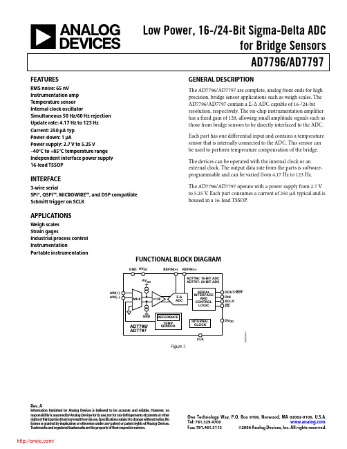
Low Power, 16-/24-Bit Sigma-Delta ADCfor Bridge SensorsAD7796/AD7797Rev. AInformation furnished by Analog Devices is believed to be accurate and reliable. However , no responsibility is assumed by Analog Devices for its use, nor for any infringements of patents or other rights of third parties that may result from its use. Specifications subject to change without notice. No license is granted by implication or otherwise under any patent or patent rights of Analog Devices. T rademarks and registered trademarks are the property of their respective owners.One Technology Way, P.O. Box 9106, Norwood, MA 02062-9106, U.S.A.Tel: 781.329.4700 Fax: 781.461.3113 ©2006 Analog Devices, Inc. All rights reserved.FEATURESRMS noise: 65 nV Instrumentation amp Temperature sensor Internal clock oscillatorSimultaneous 50 Hz/60 Hz rejection Update rate: 4.17 Hz to 123 Hz Current: 250 μA typ Power-down: 1 μAPower supply: 2.7 V to 5.25 V–40°C to +85°C temperature range Independent interface power supply 16-lead TSSOPINTERFACE3-wire serialSPI®, QSPI™, MICROWIRE™, and DSP compatible Schmitt trigger on SCLKAPPLICATIONSWeigh scales Strain gagesIndustrial process control InstrumentationPortable instrumentationGENERAL DESCRIPTIONThe AD7796/AD7797 are complete, analog front ends for high precision, bridge sensor applications such as weigh scales. The AD7796/AD7797 contain a Σ-Δ ADC capable of 16-/24-bit resolution, respectively. The on-chip instrumentation amplifier has a fixed gain of 128, allowing small amplitude signals such as those from bridge sensors to be directly interfaced to the ADC. Each part has one differential input and contains a temperature sensor that is internally connected to the ADC. This sensor can be used to perform temperature compensation of the bridge. The devices can be operated with the internal clock or an external clock. The output data rate from the parts is software-programmable and can be varied from 4.17 Hz to 123 Hz. The AD7796/AD7797 operate with a power supply from 2.7 V to 5.25 V . Each part consumes a current of 250 μA typical and is housed in a 16-lead TSSOP .FUNCTIONAL BLOCK DIAGRAMDOUT/RDY AIN(+)AIN(–)AV 06083-001Figure 1.AD7796/AD7797Rev. A | Page 2 of 24TABLE OF CONTENTSFeatures..............................................................................................1 Interface.............................................................................................1 Applications.......................................................................................1 General Description.........................................................................1 Functional Block Diagram..............................................................1 Revision History...............................................................................2 Specifications.....................................................................................3 Timing Characteristics.....................................................................5 Timing Diagrams..........................................................................6 Absolute Maximum Ratings............................................................7 Thermal Resistance......................................................................7 ESD Caution..................................................................................7 Pin Configuration and Function Descriptions.............................8 RMS Noise and Resolution Specifications....................................9 Typical Performance Characteristics...........................................10 On-Chip Registers..........................................................................11 Communication Register..........................................................11 Status Register.............................................................................12 Mode Register.............................................................................12 Configuration Register..............................................................14 Data Register...............................................................................14 ID Register...................................................................................14 Offset Register............................................................................15 Full-Scale Register......................................................................15 ADC Circuit Information..............................................................16 Overview.....................................................................................16 Digital Interface..........................................................................17 Circuit Description.........................................................................20 Analog Input Channel...............................................................20 Bipolar/Unipolar Configuration..............................................20 Data Output Coding..................................................................20 Reference.....................................................................................20 Reset.............................................................................................21 Burnout Currents.......................................................................21 AV DD Monitor.............................................................................21 Temperature Monitor................................................................21 Calibration...................................................................................21 Grounding and Layout..............................................................22 Applications.....................................................................................23 Weigh Scales................................................................................23 Outline Dimensions.......................................................................24 Ordering Guide.. (24)REVISION HISTORY8/06—Rev. 0 to Rev. A.Changes to Table 1............................................................................3 Changes to Figure 5..........................................................................8 Changes to Table 14 (13)7/06—Revision 0: Initial VersionAD7796/AD7797Rev. A | Page 3 of 24SPECIFICATIONSAV DD = 2.7 V to 5.25 V , DV DD = 2.7 V to 5.25 V , GND = 0 V , all specifications T MIN to T MAX , unless otherwise noted. Table 1.Parameter AD7796B/AD7797B 1 Unit Test Conditions/Comments ADC CHANNEL Output Update Rate 4.17 to 123 Hz nomNo Missing Codes 224 Bits min AD7797 only 16 Bits min AD7796 only Resolution See Table 7 and Table 8 RMS Noise and Update Rates See Table 6 Integral Nonlinearity ±10 ppm of FSR typOffset Error 3, 4±1 μV typ Offset Error Drift vs. Temperature 4±10 nV/°C typFull-Scale Error 3, 4, 5±10 μV typ Gain Drift vs. Temperature 4±3 ppm/°C typ Power Supply Rejection 90 dB min AIN = 1 V/128 ANALOG INPUTS Differential Input Voltage Ranges ±V REF /128 V nom V REF = REFIN(+) – REFIN(–)Absolute AIN Voltage Limits 2GND + 300 mV V min AV DD − 1.1 V max Common-Mode Voltage, V CM 0.5 V min V CM = (AIN(+) + AIN(–))/2 Analog Input CurrentAverage Input Current 2±250 pA max Update rate < 100 Hz Average Input Current Drift ±2 pA/°C typ Normal Mode Rejection 2 Internal Clock @ 50 Hz, 60 Hz 65 dB min 80 dB typ, 50 ± 1 Hz, 60 ± 1 Hz, FS[3:0] = 10106@ 50 Hz 80 dB min 90 dB typ, 50 ± 1 Hz, FS[3:0] = 10016@ 60 Hz 90 dB min 100 dB typ, 60 ± 1 Hz, FS[3:0] = 10006External Clock @ 50 Hz, 60 Hz 80 dB min 90 dB typ, 50 ± 1 Hz, 60 ± 1 Hz, FS[3:0] = 10106@ 50 Hz 94 dB min 100 dB typ, 50 ± 1 Hz, FS[3:0] = 10016@ 60 Hz 90 dB min 100 dB typ, 60 ± 1 Hz, FS[3:0] = 10006Common-Mode Rejection @ DC 90 dB min AIN = 7.81 mV @ 50 Hz, 60 Hz 290 dB min 50 ± 1 Hz, 60 ± 1 Hz, FS[3:0] = 10106@ 50 Hz, 60 Hz 290 dB min 50 ± 1 Hz (FS[3:0] = 10016), 60 ± 1 Hz,FS[3:0] = 10006REFERENCE External REFIN Voltage 2.5 V nom REFIN = REFIN(+) – REFIN(–)Reference Voltage Range 20.1 V min AV DD V maxAbsolute REFIN Voltage Limits 2GND − 30 mV V min AV DD + 30 mV V max Average Reference Input Current 400 nA/V typ Average Reference Input Current Drift ±0.03 nA/V/°C typ Normal Mode Rejection Same as for analog inputs Common-Mode Rejection 100 dB typ TEMPERATURE SENSOR Accuracy ±2 °C typ Applies if user calibrates the temperature sensor Sensitivity 0.81 mV/°C typAD7796/AD77971 Temperature range is –40°C to +85°C.2 Specification is not production tested, but is supported by characterization data at initial product release.3 Following a calibration, this error is in the order of the noise for the update rate selected.4 Recalibration at any temperature removes these errors.5 Full-scale error applies to both positive and negative full-scale and applies at the factory calibration conditions (AV DD = 4 V, T A = 25°C).6 FS[3:0] are the four bits used in the mode register to select the output word rate.7 Digital inputs equal to DV DD or GND.Rev. A | Page 4 of 24AD7796/AD7797Rev. A | Page 5 of 24TIMING CHARACTERISTICSAV DD = 2.7 V to 5.25 V , DV DD = 2.7 V to 5.25 V , GND = 0 V , Input Logic 0 = 0 V , Input Logic 1 = DV DD , unless otherwise noted.1 Sample tested during initial release to ensure compliance. All input signals are specified with t R = t F = 5 ns (10% to 90% of DV DD ) and timed from a voltage level of 1.6 V. 2See Figure 3 and Figure 4. 3These numbers are measured with the load circuit of Figure 2 and defined as the time required for the output to cross the V OL or V OH limits. 4SCLK active edge is falling edge of SCLK. 5These numbers are derived from the measured time taken by the data output to change 0.5 V when loaded with the circuit of Figure 2. The measured number is then extrapolated back to remove the effects of charging or discharging the 50 pF capacitor. This means that the times quoted in the timing characteristics are the true bus relinquish times of the parts and, as such, are independent of external bus loading capacitances. 6 RDY returns high after a read of the ADC. In single conversion mode and continuous conversion mode, the same data can be read again, if required, while RDY is high. Care should be taken to ensure that subsequent reads do not occur close to the next output update. In continuous read mode, the digital word can be read only once.WITH DV DD =5V,DV DD =3V)WITH DV DD =5V,DV DD =3V)1.6VTO OUTPUTPIN06083-002Figure 2. Load Circuit for Timing CharacterizationAD7796/AD7797Rev. A | Page 6 of 24TIMING DIAGRAMSCS SCLK I = INPUT, O= OUTPUT06083-003Figure 3. Read Cycle Timing DiagramI = INPUTCS (I)SCLK (I)DIN (I)06083-004Figure 4. Write Cycle Timing DiagramAD7796/AD7797Rev. A | Page 7 of 24ABSOLUTE MAXIMUM RATINGST A = 25°C, unless otherwise noted. Table 3.Parameter RatingAV DD to GND −0.3 V to +7 V DV DD to GND−0.3 V to +7 VAnalog Input Voltage to GND −0.3 V to AV DD + 0.3 V Reference Input Voltage to GND −0.3 V to AV DD + 0.3 V Digital Input Voltage to GND −0.3 V to DV DD + 0.3 V Digital Output Voltage to GND −0.3 V to DV DD + 0.3 V AIN/Digital Input Current10 mAOperating Temperature Range −40°C to +85°C Storage Temperature Range −65°C to +150°C Maximum Junction Temperature 150°C Lead Temperature, SolderingVapor Phase (60 sec) 215°C Infrared (15 sec)220°CStresses above those listed under Absolute Maximum Ratingsmay cause permanent damage to the device. This is a stress rating only; functional operation of the device at these or any other conditions above those indicated in the operationalsection of this specification is not implied. Exposure to absolute maximum rating conditions for extended periods may affect device reliability. THERMAL RESISTANCEθJA is specified for the worst-case conditions, that is, a device soldered in a circuit board for surface-mount packages. Table 4.Package Type θJA θJC Unit TSSOP 128 14 °C/WESD CAUTIONAD7796/AD7797Rev. A | Page 8 of 24PIN CONFIGURATION AND FUNCTION DESCRIPTIONSNC =NO CONNECT06083-005Figure 5. Pin ConfigurationAD7796/AD7797Rev. A | Page 9 of 24RMS NOISE AND RESOLUTION SPECIFICATIONSTable 6 shows the rms noise of the AD7796/AD7797 for some of the update rates. The numbers given are for the bipolar input range with an external 2.5 V reference. These numbers aretypical and are generated with a differential input voltage of 0 V . Table 7 and Table 8 show the effective resolution, while the output peak-to-peak (p-p) resolution is shown in brackets. It is important to note that the effective resolution is calculatedusing the rms noise, while the p-p resolution is based on the p-p noise. The p-p resolution represents the resolution for which there is no code flicker. These numbers are typical and are rounded to the nearest 0.5 LSB.Table 6. RMS Noise (μV) vs. Output Update Rate for the AD7796/AD7797 Using a 2.5 V ReferenceUpdate Rate (Hz) RMS Noise (μV) 4.17 0.065 6.25 0.07 8.33 0.08 10 0.09 12.5 0.1 16.7 0.12 33.2 0.17 50 0.21 62 0.23 1230.43Table 7. Typical Resolution (Bits) vs. Output Update Rate for the AD7797 Using a 2.5 V ReferenceUpdate Rate (Hz) Effective Bits (p-p) 4.17 19 (16.5) 6.25 19 (16.5) 8.33 19 (16) 10 18.5 (16) 12.5 18.5 (16) 16.7 18.5 (15.5) 33.2 18 (15) 50 17.5 (15) 62 17.5 (14.5) 12316.5 (13.5)Table 8. Typical Resolution (Bits) vs. Output Update Rate for the AD7796 Using a 2.5 V ReferenceUpdate Rate (Hz) Effective Bits (p-p) 4.17 16 (16) 6.25 16 (16) 8.33 16 (16) 10 16 (16) 12.5 16 (16) 16.7 16 (15.5) 33.2 16 (15) 50 16 (15) 62 16 (14.5) 12316 (13.5)AD7796/AD7797Rev. A | Page 10 of 24SAMPLES(µV )TYPICAL PERFORMANCE CHARACTERISTICS60–4001000 2.0–2.001000SAMPLES(µV )40200–2010020030040050060070080090006083-006Figure 6. AD7797 Noise (V REF = AV DD , Update Rate = 16.7 Hz)17.5083884858388744CODEO C C U R R E N C E15.012.510.07.55.02.5838855083886008388650838870006083-007Figure 7. AD7797 Noise Distribution Histogram(V REF = AV DD , Update Rate = 16.7 Hz) 1002003004005006007008009001.51.00.50–0.5–1.0–1.506083-008Figure 8. AD7797 Noise (V REF = AV DD , Update Rate = 4.17 Hz)35083885538388662CODEO C C U R R E N C E83885808388600838862083886403025201510506083-009Figure 9. AD7797 Noise Distribution Histogram(V REF = AV DD , Update Rate = 4.17 Hz)分销商库存信息:ANALOG-DEVICESAD7796BRUZ AD7797BRUZ AD7796BRUZ-REEL AD7797BRUZ-REEL EVAL-AD7797EBZ。
HT75XXHigh Driver RegulatorSelection TablePart No.Output VoltageToleranceHT7530 3.0V ±5%HT7533 3.3V ±5%HT7536 3.6V ±5%HT7544 4.4V ±5%HT7550 5.0V ±5%HT75808.0V±5%1May 2,2000Features·Low power consumption ·Low voltage drop·Low temperature coefficient ·High input voltage (up to 24V)·High output current :100mA (P d £250mW)·TO-92and SOT-89packageApplications·Battery-powered equipment ·Communication equipment·Audio/Video equipmentGeneral DescriptionThe HT75XX series is a set of three-terminal high current low voltage regulator imple-mented in CMOS technology.They can deliver 100mA output current and allow an input volt-age as high as 24V .They are available with sev-eral fixed output voltages ranging from 3.0V to 8V .CMOS technology ensures low voltage drop and low quiescent current.Although designed primarily as fixed voltage regulators,these devices can be used with ex-ternal components to obtain variable voltages and currents.Block DiagramPin AssignmentHT75XX2May 2,2000Pad Assignment Pad Coordinates Unit:m mPad No.X Y1-506.50-589.50261.00-582.503510.50-585.50 Chip size:1390´1530(m m)2*The IC substrate should be connected to VDD in the PCB layout artwork.Absolute Maximum RatingsSupply Voltage...............................-0.3V to26V Storage Temperature.................-50°C to125°C Power Consumption..............................250mW Operating Temperature..................0°C to70°CNote:These are stress ratings only.Stresses exceeding the range specified under²Absolute Maxi-mum Ratings²may cause substantial damage to the device.Functional operation of this device at other conditions beyond those listed in the specification is not implied and prolonged expo-sure to extreme conditions may affect device reliability.3May2,2000Electrical CharacteristicsHT7530,+3.0V output type Ta=25°CHT7533,+3.3V output type Ta=25°C4May2,2000HT7544,+4.4V output type Ta=25°C5May2,2000HT7580,+8.0V output type Ta=25°C6May2,2000Application CircuitsBasic circuitHigh output current positive voltage regulatorShort-Circuit protection for Tr1HT75XX7May 2,2000Circuit for increasing output voltageV=V(1+R2R1)+I R2OUT XX SS Circuit for increasing output voltageV=V+VOUT XX D1 Constant current regulatorI=VR +IOUTXXASS8May2,2000Dual supply9May2,200010May 2,2000Copyright ã2000by HOLTEK SEMICONDUCTOR INC.The information appearing in this Data Sheet is believed to be accurate at the time of publication.However,Holtek assumes no responsibility arising from the use of the specifications described.The applications mentioned herein are used solely for the purpose of illustration and Holtek makes no warranty or representation that such applications will be suitable without further modification,nor recommends the use of its products for application that may pres-ent a risk to human life due to malfunction or otherwise.Holtek reserves the right to alter its products without prior notification.For the most up-to-date information,please visit our web site at .Holtek Semiconductor Inc.(Headquarters)No.3Creation Rd.II,Science-based Industrial Park,Hsinchu,Taiwan,R.O.C.Tel:886-3-563-1999Fax:886-3-563-1189Holtek Semiconductor Inc.(Taipei Office)5F,No.576,Sec.7Chung Hsiao E.Rd.,Taipei,Taiwan,R.O.C.Tel:886-2-2782-9635Fax:886-2-2782-9636Fax:886-2-2782-7128(International sales hotline)Holtek Semiconductor (Hong Kong)Ltd.RM.711,Tower 2,Cheung Sha Wan Plaza,833Cheung Sha Wan Rd.,Kowloon,Hong Kong Tel:852-2-745-8288Fax:852-2-742-8657。
November 6, 2007 LMP7717/LMP771888 MHz, Precision, Low Noise, 1.8V CMOS Input, Decompensated Operational AmplifierGeneral DescriptionThe LMP7717 (single) and the LMP7718 (dual) low noise, CMOS input operational amplifiers offer a low input voltage noise density of 5.8 nV/ while consuming only 1.15 mA (LMP7717) of quiescent current. The LMP7717/LMP7718 are stable at a gain of 10 and have a gain bandwidth (GBW) product of 88 MHz. The LMP7717/LMP7718 have a supply voltage range of 1.8V to 5.5V and can operate from a single supply. The LMP7717/LMP7718 each feature a rail-to-rail output stage. Both amplifiers are part of the LMP® precision amplifier family and are ideal for a variety of instrumentation applications.The LMP7717 family provides optimal performance in low voltage and low noise systems. A CMOS input stage, with typical input bias currents in the range of a few femto-Am-peres, and an input common mode voltage range, which includes ground, make the LMP7717/LMP7718 ideal for low power sensor applications where high speeds are needed. The LMP7717/LMP7718 are manufactured using National’s advanced VIP50 process. The LMP7717 is offered in either a 5-Pin SOT23 or an 8-Pin SOIC package. The LMP7718 is offered in either the 8-Pin SOIC or the 8-Pin MSOP.Features(Typical 5V supply, unless otherwise noted)■Input offset voltage±150 µV (max)■Input referred voltage noise 5.8 nV/√Hz ■Input bias current100 fA ■Gain bandwidth product88 MHz ■Supply voltage range 1.8V to 5.5V ■Supply current per channel—LMP7717 1.15 mA —LMP7718 1.30 mA ■Rail-to-Rail output swing—@ 10 kΩ load25 mV from rail —@ 2 kΩ load45 mV from rail ■Guaranteed 2.5V and 5.0V performance■Total harmonic distortion0.04% @1 kHz, 600Ω■Temperature range−40°C to 125°C Applications■ADC interface■Photodiode amplifiers■Active filters and buffers■Low noise signal processing■Medical instrumentation■Sensor interface applicationsTypical Application30010869 Photodiode Transimpedance Amplifier30010839 Input Referred Voltage Noise vs. FrequencyLMP® is a registered trademark of National Semiconductor Corporation.© 2007 National Semiconductor LMP7717/LMP7718 88 MHz, Precision, Low Noise, 1.8V CMOS Input, Decompensated Operational AmplifierAbsolute Maximum Ratings (Note 1)If Military/Aerospace specified devices are required,please contact the National Semiconductor Sales Office/Distributors for availability and specifications.ESD Tolerance (Note 2) Human Body Model 2000V Machine Model200V V IN Differential±0.3V Supply Voltage (V + – V −) 6.0VInput/Output Pin Voltage V + +0.3V, V − −0.3V Storage Temperature Range −65°C to 150°CJunction Temperature (Note 3)+150°CSoldering Information Infrared or Convection (20 sec)235°C Wave Soldering Lead Temp (10 sec)260°COperating Ratings(Note 1)Temperature Range (Note 3)−40°C to 125°C Supply Voltage (V + – V −) −40°C ≤ T A ≤ 125°C 2.0V to 5.5V 0°C ≤ T A ≤ 125°C1.8V to 5.5V Package Thermal Resistance (θJA (Note 3)) 5-Pin SOT23180°C/W 8-Pin SOIC 190°C/W 8-Pin MSOP236°C/W2.5V Electrical Characteristics(Note 4)Unless otherwise specified, all limits are guaranteed for T A = 25°C, V + = 2.5V, V − = 0V, V CM = V +/2 = V O . Boldface limits apply at the temperature extremes.Symbol ParameterConditionsMin (Note 6)Typ (Note 5)Max (Note 6)UnitsV OS Input Offset Voltage±20±180±480µV TC V OS Input Offset Average Drift (Note 7)LMP7717 −1.0±4μV/°CLMP7718−1.8I BInput Bias CurrentV CM = 1.0V (Notes 8, 9)−40°C ≤ T A ≤ 85°C 0.05125pA−40°C ≤ T A ≤ 125°C0.051100I OS Input Offset CurrentV CM = 1.0V (Note 9).0060.550pA CMRR Common Mode Rejection Ratio 0V ≤ V CM ≤ 1.4V 838094 dBPSRRPower Supply Rejection Ratio2.0V ≤ V + ≤ 5.5V, V CM = 0V 8580100dB1.8V ≤ V + ≤ 5.5V, V CM = 0V8598 CMVR Input Common-Mode Voltage RangeCMRR ≥ 60 dB CMRR ≥ 55 dB −0.3−0.31.51.5V A VOLOpen Loop GainV OUT = 0.15V to 2.2V,R L = 2 k Ω to V +/2LMP7717888298 dB LMP7718848092 V OUT = 0.15V to 2.2V,R L = 10 k Ω to V +/2LMP77179288110 LMP7718908695 V OUTOutput Swing HighR L = 2 k Ω to V +/2 257077mV from rail R L = 10 k Ω to V +/2206066Output Swing LowR L = 2 k Ω to V +/2 307073R L = 10 k Ω to V +/2156062 2L M P 7717/L M P 7718I OUTOutput Short Circuit CurrentSourcing to V −V IN = 200 mV (Note 10)363047 mASinking to V +V IN = –200 mV (Note 10)7.5515 I SSupply Current per AmplifierLMP77170.95 1.301.65mALMP7718 per channel1.1 1.51.85SR Slew RateA V = +10, Rising (10% to 90%)32 V/μs A V = +10, Falling (90% to 10%)24 GBWP Gain Bandwidth Product A V = +10, R L = 10 k Ω 88 MHz e n Input-Referred Voltage Noise f = 1 kHz 6.2 nV/i n Input-Referred Current Noise f = 1 kHz0.01 pA/THD+NTotal Harmonic Distortion +Noisef = 1 kHz, A V = 1, R L = 600Ω0.01%5V Electrical Characteristics(Note 4)Unless otherwise specified, all limits are guaranteed for T A = 25°C, V + = 5V, V − = 0V, V CM = V +/2 = V O . Boldface limits apply at the temperature extremes.Symbol ParameterConditionsMin (Note 6)Typ (Note 5)Max (Note 6)UnitsV OS Input Offset Voltage±10±150±450µV TC V OS Input Offset Average Drift (Note 7)LMP7717 −1.0±4μV/°CLMP7718−1.8I BInput Bias CurrentV CM = 2.0V (Notes 8, 9)−40°C ≤ T A ≤ 85°C 0.1125pA−40°C ≤ T A ≤ 125°C0.11100I OS Input Offset CurrentV CM = 2.0V (Note 9).010.550pA CMRR Common Mode Rejection Ratio 0V ≤ V CM ≤ 3.7V 8580100 dBPSRRPower Supply Rejection Ratio2.0V ≤ V + ≤ 5.5V, V CM = 0V 8580100dB1.8V ≤ V + ≤ 5.5V, V CM = 0V8598 CMVR Input Common-Mode Voltage RangeCMRR ≥ 60 dB CMRR ≥ 55 dB −0.3−0.344V A VOLOpen Loop GainV OUT = 0.3V to 4.7V,R L = 2 k Ω to V +/2LMP77178882107 dB LMP7718848090 V OUT = 0.3V to 4.7V,R L = 10 k Ω to V +/2LMP77179288110 LMP7718908695LMP7717/LMP7718V OUTOutput Swing HighR L = 2 k Ω to V +/2LMP7717 357077mV from railLMP7718458077R L = 10 k Ω to V +/2256066Output Swing LowR L = 2 k Ω to V +/2LMP7717 427073LMP7718508078R L = 10 k Ω to V +/2256066I OUTOutput Short Circuit CurrentSourcing to V −V IN = 200 mV (Note 10)463860 mA Sinking to V +V IN = –200 mV (Note 10)10.56.521 I SSupply Current per AmplifierLMP77171.15 1.401.75mALMP7718 per channel1.30 1.702.05SR Slew RateA V = +10, Rising (10% to 90%) 35 V/μs A V = +10, Falling (90% to 10%)28 GBWP Gain Bandwidth Product A V = +10, R L = 10 k Ω 88 MHz e n Input-Referred Voltage Noise f = 1 kHz 5.8 nV/i n Input-Referred Current Noise f = 1 kHz0.01 pA/THD+NTotal Harmonic Distortion +Noisef = 1 kHz, A V = 1, R L = 600Ω0.01%Note 1:Absolute Maximum Ratings indicate limits beyond which damage to the device may occur. Operating Ratings indicate conditions for which the device is intended to be functional, but specific performance is not guaranteed. For guaranteed specifications and the test conditions, see the Electrical Characteristics Tables.Note 2:Human Body Model, applicable std. MIL-STD-883, Method 3015.7. Machine Model, applicable std. JESD22-A115-A (ESD MM std. of JEDEC)Field-Induced Charge-Device Model, applicable std. JESD22-C101-C (ESD FICDM std. of JEDEC).Note 3:The maximum power dissipation is a function of T J(MAX), θJA . The maximum allowable power dissipation at any ambient temperature is P D = (T J(MAX) - T A )/θJA . All numbers apply for packages soldered directly onto a PC Board.Note 4:Electrical Table values apply only for factory testing conditions at the temperature indicated. Factory testing conditions result in very limited self-heating of the device such that T J = T A . No guarantee of parametric performance is indicated in the electrical tables under conditions of internal self-heating where T J >T A .Note 5:Typical values represent the most likely parametric norm as determined at the time of characterization. Actual typical values may vary over time and will also depend on the application and configuration. The typical values are not tested and are not guaranteed on shipped production material.Note 6:Limits are 100% production tested at 25°C. Limits over the operating temperature range are guaranteed through correlations using the statistical quality control (SQC) method.Note 7:Offset voltage average drift is determined by dividing the change in V OS by temperature change.Note 8:Positive current corresponds to current flowing into the device.Note 9:Input bias current and input offset current are guaranteed by designNote 10:The short circuit test is a momentary test, the short circuit duration is 1.5 ms. 4L M P 7717/L M P 7718Connection Diagrams5-Pin SOT23 (LMP7717)30010801Top View8-Pin SOIC (LMP7717)30010885Top View8-Pin SOIC/MSOP (LMP7718)30010802Ordering InformationPackage Part Number Package MarkingTransport Media NSC Drawing5-Pin SOT23LMP7717MF AT4A 1k Units Tape and Reel MF05A LMP7717MFE 250 Units Tape and Reel LMP7717MFX 3k Units Tape and Reel8-Pin SOICLMP7717MA LMP7717MA95 Units/Rail M08A LMP7717MAE250 Units Tape and Reel LMP7717MAX 2.5k Units Tape and ReelLMP7718MA LMP7718MA 95 Units/Rail LMP7718MAE 250 Units Tape and Reel LMP7718MAX 2.5k Units Tape and Reel 8-Pin MSOPLMP7718MMAP4A 1k Units Tape and Reel MUA08A LMP7718MME 250 Units Tape and Reel LMP7718MMX3.5k Units Tape and ReelLMP7717/LMP7718Typical Performance CharacteristicsUnless otherwise specified, T A = 25°C, V – = 0, V + = 5V,V S = V + - V −, V CM = V S /2.TCV OS Distribution (LMP7717)30010890Offset Voltage Distribution30010891TCV OS Distribution (LMP7717)30010892Offset Voltage Distribution30010893Supply Current vs. Supply Voltage (LMP7717)30010805V OS vs. V CM30010809 6L M P 7717/L M P 7718V OS vs. V CM30010851V OS vs. V CM30010811V OS vs. Supply Voltage30010812Slew Rate vs. Supply Voltage30010852Input Bias Current vs. V CM 30010862Input Bias Current vs. V CM30010887LMP7717/LMP7718Sourcing Current vs. Supply Voltage30010820Sinking Current vs. Supply Voltage30010819Sourcing Current vs. Output Voltage 30010850Sinking Current vs. Output Voltage30010854Positive Output Swing vs. Supply Voltage 30010817Negative Output Swing vs. Supply Voltage30010815 8L M P 7717/L M P 7718Positive Output Swing vs. Supply Voltage30010816Negative Output Swing vs. Supply Voltage30010814Positive Output Swing vs. Supply Voltage30010818Negative Output Swing vs. Supply Voltage30010813Input Referred Voltage Noise vs. Frequency30010839Overshoot and Undershoot vs. CLOAD30010830LMP7717/LMP7718THD+N vs. Frequency30010826THD+N vs. Frequency30010804THD+N vs. Peak-to-Peak Output Voltage (V OUT )30010874THD+N vs. Peak-to-Peak Output Voltage (V OUT )30010875Open Loop Gain and Phase 30010806Closed Loop Output Impedance vs. Frequency30010832 10L M P 7717/L M P 7718Crosstalk Rejection30010880Small Signal Transient Response, A V = +1030010853Large Signal Transient Response, A V = +1030010855Small Signal Transient Response, A V = +1030010857Large Signal Transient Response, A V = +1030010863PSRR vs. Frequency30010870LMP7717/LMP7718CMRR vs. Frequency30010856Input Common Mode Capacitance vs. V CM30010876L M P 7717/L M P 7718Application InformationADVANTAGES OF THE LMP7717/LMP7718Wide Bandwidth at Low Supply CurrentThe LMP7717/LMP7718 are high performance op amps that provide a GBW of 88 MHz with a gain of 10 while drawing a low supply current of 1.15 mA. This makes them ideal for pro-viding wideband amplification in data acquisition applications. With the proper external compensation the LMP7717 can be operated at gains of ±1 and still maintain much faster slew rates than comparable unity gain stable amplifiers. The in-crease in bandwidth and slew rate is obtained without any additional power consumption over the LMP7715.Low Input Referred Noise and Low Input Bias Current The LMP7717/LMP7718 have a very low input referred volt-age noise density (5.8 nV/ at 1 kHz). A CMOS input stage ensures a small input bias current (100 fA) and low input re-ferred current noise (0.01 pA/). This is very helpful in maintaining signal integrity, and makes the LMP7717/ LMP7718 ideal for audio and sensor based applications.Low Supply VoltageThe LMP7717 and the LMP7718 have performance guaran-teed at 2.5V and 5V supply. These parts are guaranteed to be operational at all supply voltages between 2.0V and 5.5V, for ambient temperatures ranging from −40°C to 125°C, thus utilizing the entire battery lifetime. The LMP7717/LMP7718 are also guaranteed to be operational at 1.8V supply voltage, for temperatures between 0°C and 125°C optimizing their us-age in low-voltage applications.RRO and Ground SensingRail-to-Rail output swing provides the maximum possible dy-namic range. This is particularly important when operating at low supply voltages. An innovative positive feedback scheme is used to boost the current drive capability of the output stage. This allows the LMP7717/LMP7718 to source more than 40 mA of current at 1.8V supply. This also limits the per-formance of the these parts as comparators, and hence the usage of the LMP7717 and the LMP7718 in an open-loop configuration is not recommended. The input common-mode range includes the negative supply rail which allows direct sensing at ground in single supply operation.Small SizeThe small footprints of the LMP7717 packages and the LMP7718 packages save space on printed circuit boards, and enable the design of smaller electronic products, such as cel-lular phones, pagers, or other portable systems. Long traces between the signal source and the op amp make the signal path more susceptible to noise pick up.The physically smaller LMP7717 or LMP7718 packages allow the op amp to be placed closer to the signal source, thus re-ducing noise pickup and maintaining signal integrity.USING THE DECOMPENSATED LMP7717Advantages of Decompensated Op AmpA unity gain stable op amp, which is fully compensated, is designed to operate with good stability down to gains of ±1. The large amount of compensation does provide an op amp that is relatively easy to use; however, a decompensated op amp is designed to maximize the bandwidth and slew rate without any additional power consumption. This can be very advantageous.The LMP7717/LMP7718 require a gain of ±10 to be stable.However, with an external compensation network (a simpleRC network) these parts can be stable with gains of ±1 andstill maintain the higher slew rate. Looking at the Bode plotsfor the LMP7717 and its closest equivalent unity gain stableop amp, the LMP7715, one can clearly see the increased bandwidth of the LMP7717. Both plots are taken with a par-allel combination of 20 pF and 10 kΩ for the output load.30010822FIGURE 1. LMP7717 AVOLvs. Frequency30010823FIGURE 2. LMP7715 AVOLvs. FrequencyFigure 1 shows the much larger 88 MHz bandwidth of theLMP7717 as compared to the 17 MHz bandwidth of theLMP7715 shown in Figure 2. The decompensated LMP7717has five times the bandwidth of the LMP7715.What is a Decompensated Op Amp?The differences between the unity gain stable op amp and the decompensated op amp are shown in Figure 3. This Bode plot assumes an ideal two pole system. The dominant pole of thedecompensated op amp is at a higher frequency, f1, as com-pared to the unity gain stable op amp which is at fdas shownin Figure 3. This is done in order to increase the speed capa-bility of the op amp while maintaining the same power dissi-pation of the unity gain stable op amp. The LMP7717/LMP7718 have a dominant pole at 8.6 Hz. The unity gain sta-ble LMP7715/LMP7716 have their dominant pole at 1.6 Hz.LMP7717/LMP771830010824FIGURE 3. Open Loop Gain for Unity Gain Stable Op Ampand Decompensated Op Amp Having a higher frequency for the dominate pole will result in:1.The DC open loop gain (A VOL ) extending to a higherfrequency.2. A wider closed loop bandwidth.3.Better slew rate due to reduced compensationcapacitance within the op amp.The second open loop pole (f 2) for the LMP7717/LMP7718occurs at 45 MHz. The unity gain (f u ’) occurs after the second pole at 51 MHz. An ideal two pole system would give a phase margin of 45° at the location of the second pole. The LMP7717/LMP7718 have parasitic poles close to the second pole, giving a phase margin closer to 0°. Therefore it is nec-essary to operate the LMP7717/LMP7718 at a closed loop gain of 10 or higher, or to add external compensation in order to assure stability.For the LMP7715, the gain bandwidth product occurs at 17MHz. The curve is constant from f d to f u which occurs before the second pole.For the LMP7717/LMP7718 the GBW = 88 MHz and is con-stant between f 1 and f 2. The second pole at f 2 occurs before A VOL =1. Therefore f u ’ occurs at 51 MHz, well before the GBW frequency of 88 MHz. For decompensated op amps the unity gain frequency and the GBW are no longer equal. G min is the minimum gain for stability and for the LMP7717/LMP7718 this is a gain of 10 or 20 dB.Input Lead-Lag CompensationThe recommended technique which allows the user to com-pensate the LMP7717/LMP7718 for stable operation at any gain is lead-lag compensation. The compensation compo-nents added to the circuit allow the user to shape the feedback function to make sure there is sufficient phase margin when the loop gain is as low as 0 dB and still maintain the advan-tages over the unity gain op amp. Figure 4 shows the lead-lag configuration. Only R C and C are added for the necessary compensation.30010825FIGURE 4. LMP7717 with Lead-Lag Compensation forInverting ConfigurationTo cover how to calculate the compensation network values it is necessary to introduce the term called the feedback factor or F. The feedback factor F is the feedback voltage V A -V B across the op amp input terminals relative to the op amp out-put voltage V OUT .From feedback theory the classic form of the feedback equa-tion for op amps is:A is the open loop gain of the amplifier and AF is the loop gain.Both are highly important in analyzing op amps. Normally AF >>1 and so the above equation reduces to:Deriving the equations for the lead-lag compensation is be-yond the scope of this datasheet. The derivation is based on the feedback equations that have just been covered. The in-verse of feedback factor for the circuit in Figure 4 is:(1)where 1/F's pole is located at(2)1/F's zero is located at(3)L M P 7717/L M P 7718(4)The circuit gain for Figure 4 at low frequencies is −R F /R IN , but F , the feedback factor is not equal to the circuit gain. The feedback factor is derived from feedback theory and is the same for both inverting and non-inverting configurations. Yes,the feedback factor at low frequencies is equal to the gain for the non-inverting configuration.(5)From this formula, we can see that•1/F's zero is located at a lower frequency compared with 1/F's pole.•1/F's value at low frequency is 1 + R F /R IN .•This method creates one additional pole and one additional zero.•This pole-zero pair will serve two purposes:—To raise the 1/F value at higher frequencies prior to its intercept with A, the open loop gain curve, in order to meet the G min = 10 requirement. For the LMP7717some overcompensation will be necessary for good stability.—To achieve the previous purpose above with no additional loop phase delay.Please note the constraint 1/F ≥ G min needs to be satisfied only in the vicinity where the open loop gain A and 1/F inter-sect; 1/F can be shaped elsewhere as needed. The 1/F pole must occur before the intersection with the open loop gain A.In order to have adequate phase margin, it is desirable to fol-low these two rules:Rule 11/F and the open loop gain A should intersect at thefrequency where there is a minimum of 45° of phase margin. When over-compensation is required the in-tersection point of A and 1/F is set at a frequency where the phase margin is above 45°, therefore in-creasing the stability of the circuit.Rule 21/F’s pole should be set at least one decade belowthe intersection with the open loop gain A in order to take advantage of the full 90° of phase lead brought by 1/F’s pole which is F’s zero. This ensures that the effect of the zero is fully neutralized when the 1/F and A plots intersect each other.Calculating Lead-Lag Compensation for LMP7717Figure 5 is the same plot as Figure 1, but the A VOL and phase curves have been redrawn as smooth lines to more readily show the concepts covered, and to clearly show the key pa-rameters used in the calculations for lead-lag compensation.30010848FIGURE 5. LMP7717/LMP7718 Simplified Bode Plot To obtain stable operation with gains under 10 V/V the open loop gain margin must be reduced at high frequencies to where there is a 45° phase margin when the gain margin of the circuit with the external compensation is 0 dB. The pole and zero in F, the feedback factor, control the gain margin at the higher frequencies. The distance between F and A VOL is the gain margin; therefore, the unity gain point (0 dB) is where F crosses the A VOL curve.For the example being used R IN = R F for a gain of −1. There-fore F = 6 dB at low frequencies. At the higher frequencies the minimum value for F is 18 dB for 45° phase margin. From Equation 5 we have the following relationship:Now set R F = R IN = R. With these values and solving for R C we have R C = R/5.9. Note that the value of C does not affect the ratio between the resistors. Once the value of the resistors is set, then the position of the pole in F must be set. A 2 k Ωresistor is used for R F and R IN in this design. Therefore the value for R C is set at 330Ω, the closest standard value for 2k Ω/5.9.Rewriting Equation 2 to solve for the minimum capacitor value gives the following equation:C = 1/(2πf p R C )The feedback factor curve, F , intersects the A VOL curve at about 12 MHz. Therefore the pole of F should not be any larger than 1.2 MHz. Using this value and R C = 330Ω the minimum value for C is 390 pF. Figure 6 shows that there is too much overshoot, but the part is stable. Increasing C to 2.2nF did not improve the ringing, as shown in Figure 7.LMP7717/LMP771830010803FIGURE 6. First Try at Compensation, Gain = −130010807FIGURE 7. C Increased to 2.2 nF, Gain = −1Some over-compensation appears to be needed for the de-sired overshoot characteristics. Instead of intersecting the A VOL curve at 18 dB, 2 dB of over-compensation will be used,and the A VOL curve will be intersected at 20 dB. Using Equa-tion 5 for 20 dB, or 10 V/V, the closest standard value of R C is 240Ω. The following two waveforms show the new resistor value with C = 390 pF and 2.2 nF. Figure 9 shows the final compensation and a very good response for the 1 MHz square wave.30010808FIGURE 8. R C = 240Ω and C = 390 pF, Gain = −130010810FIGURE 9. R C = 240Ω and C = 2.2 nF, Gain = −1To summarize, the following steps were taken to compensate the LMP7717 for a gain of −1:1.Values for R c and C were calculated from the Bode plotto give an expected phase margin of 45°. The values were based on R IN = R F = 2 k Ω. These calculations gave R c = 330Ω and C = 390 pF.2.To reduce the ringing C was increased to 2.2 nF whichmoved the pole of F, the feedback factor, farther away from the A VOL curve.3.There was still too much ringing so 2 dB of over-compensation was added to F. This was done by decreasing R C to 240Ω.The LMP7715 is the fully compensated part which is compa-rable to the LMP7717. Using the LMP7715 in the same setup,but removing the compensation network, provided the re-sponse shown in Figure 10 .30010821FIGURE 10. LMP7715 ResponseFor large signal response the rise and fall times are dominat-ed by the slew rate of the op amps. Even though both parts are quite similar the LMP7717 will give rise and fall times about 2.5 times faster than the LMP7715. This is possible because the LMP7717 is a decompensated op amp and even though it is being used at a gain of −1, the speed is preserved by using a good technique for external compensation.L M P 7717/L M P 7718Non-Inverting CompensationFor the non-inverting amp the same theory applies for estab-lishing the needed compensation. When setting the inverting configuration for a gain of −1, F has a value of 2. For the non-inverting configuration both F and the actual gain are the same, making the non-inverting configuration more difficult to compensate. Using the same circuit as shown in Figure 4, but setting up the circuit for non-inverting operation (gain of +2)results in similar performance as the inverting configuration with the inputs set to half the amplitude to compensate for the additional gain. Figure 11 below shows the results.30010882FIGURE 11. R C = 240Ω and C = 2.2 nF, Gain = +230010883FIGURE 12. LMP7715 Response Gain = +2The response shown in Figure 11 is close to the response shown in Figure 9. The part is actually slightly faster in the non-inverting configuration. Decreasing the value of R C to around 200Ω can decrease the negative overshoot but will have slightly longer rise and fall times. The other option is to add a small resistor in series with the input signal. Figure 12shows the performance of the LMP7715 with no compensa-tion. Again the decompensated parts are almost 2.5 times faster than the fully compensated op amp.The most difficult op amp configuration to stabilize is the gain of +1. With proper compensation the LMP7717/LMP7718 can be used in this configuration and still maintain higher speedsthan the fully compensated parts. Figure 13 shows the gain =1, or the buffer configuration, for these parts.30010884FIGURE 13. LMP7717 with Lead-Lag Compensation forNon-Inverting Configuration Figure 13 is the result of using Equation 5 and additional ex-perimentation in the lab. R P is not part of Equation 5, but it is necessary to introduce another pole at the input stage for good performance at gain = +1. Equation 5 is shown below with R IN = ∞.Using 2 k Ω for R F and solving for R C gives R C = 2000/6.9 =290Ω. The closest standard value for R C is 300Ω. After some fine tuning in the lab R C = 330Ω and R P = 1.5 k Ω were chosen as the optimum values. R P together with the input capacitance at the non-inverting pin inserts another pole into the compen-sation for the LMP7717. Adding this pole and slightly reducing the compensation for 1/F (using a slightly higher resistor value for R C ) gives the optimum response for a gain of +1. Figure 14 is the response of the circuit shown in Figure 13. Figure 15 shows the response of the LMP7715 in the buffer config-uration with no compensation and R P = R F = 0.30010888FIGURE 14. R C = 330Ω and C = 10 nF, Gain = +1LMP7717/LMP7718。
Application Report SLAA625C – May 2014 – Revised July 20151 PurePath™ Smart Amp Overview (TAS5766M/68M)Jorge ArbonaHigh Performance Analog / AudioABSTRACTPurePath™ Smart Amp provides powerful tools to make speaker characterization and tuning easy.Smart Amp replaces traditional continuous power design principles and hardware basedspeaker protection methods with algorithms that allow significant increases in peak poweroutput, loudness and sound quality relative to conventional amplifiers.Smart Amp tools allow developers to understand how speakers are performing in thesystem and then make informed decisions to improve performance. The algorithms,characterization and tuning tools allow developers to overcome a wide variety of audiochallenges.WARNING: EXPORT NOTICERecipient agrees to not knowingly export or re-export, directly or indirectly, any product or technical data (as defined by the U.S., EU, and other Export Administration Regulations) including software, or any controlled product restricted by other applicable nationalregulations, received from Disclosing party under this Agreement, or any direct product of such technology, to any destination to which such export or re-export is restricted or prohibited by U.S. or other applicable laws, without obtaining prior authorization from U.S. Department of Commerce and other competent Government authorities to the extent required by those laws. This provision shall survive termination or expiration of this Agreement.According to our best knowledge of the state and end-use of this product or technology, and in compliance with the export control regulations of dual-use goods in force in the origin and exporting countries, this technology is classified as follows:US ECCN: 3E991EU ECCN: EAR99And may require export or re-export license for shipping it in compliance with the applicable regulations of certain countries.SLAA625C2 PurePath™ Smart Amp Overview (TAS5766M/68M)Contents1 Supported Smart Amp Devices (3)2 What is Smart Amp? (4)2.1 Smart Amp Features (5)3 Smart Amp Development Overview (6)4 What’s Needed (7)4.1 Obtaining TI Hardware and Software (8)4.2 Miscellaneous Equipment (9)5 Support (10)Revision History (11)Trademarks (11)FiguresFigure 1. PurePath™ Smart Amp Block Diagram (4)Figure 2. Smart Amp Development Overview (6)Figure 3.mySecureSoftware Page ................................................................................................. 8 TablesTable 1. Equipment and Software (7)Table 2. Miscellaneous Equipment (9)Table 3. Microphones Tested for Smart SPL and Passive Radiator Systems (9)Revision History (11)SLAA625C PurePath™ Smart Amp Overview (TAS5766M/68M) 3 1 Supported Smart Amp DevicesThis document supports the following Smart Amp devices:1. TAS5766M2. TAS5768MSLAA625C4 PurePath™ Smart Amp Overview (TAS5766M/68M)2 What is Smart Amp?Conventional hardware-based speaker protection matches the continuous power output of the audio amplifier with the speaker output rating and sometimes incorporates high pass filtering to prevent over-excursion. PurePath™ Smart Amp replaces hardware based speaker protection methods with predictive algorithms, speaker characterization tools and real-time signal monitoring to increase the peak output of the speaker without damage.The first implementation step of Smart Amp based audio solutions is characterizing the speaker with TI’s PurePath™ Console 3 and the PurePath™ Learning Board . These are powerful, easy-to-use tools designed specifically to simplify system level characterization, tuning andimplementation. The characterization process creates a digital model of the speaker based on thermal, electro-mechanical and acoustic parameters.The output of the characterization process is an initial set of coefficients that define the Safe Operating Area (SOA) which establishes the boundaries of maximum speaker diaphragm excursion and voice-coil temperature during operation. If the SOA is set correctly, the audioengineer need not worry about speaker damage during the audio tuning process – depending on how hard the system is pushed audio might sound more or less desirable, but speaker safety is ensured if configured properly.AudioInputFigure 1. PurePath™ Smart Amp Block DiagramPurePath™ Smart Amp technology enables significant sound quality and system reliability improvements while reducing component size and cost. The PurePath™ Console 3 graphical user interface and Learning Board speaker characterization hardware provide simpleconfiguration of advanced properties fully describing an audio system’s acoustical, electrical, thermal and reliability capabilities and simplifying system level characterization, tuning and integration.SLAA625CPurePath™ Smart Amp Overview (TAS5766M/68M) 52.1 Smart Amp FeaturesSmart BassBass can easily be extended into any alignmentautomatically. As signal amplitude is increased inthe bass region, Smart Bass automaticallymorphs the response to accommodate for larger excursion.Smart SPLHigh-frequency behavior of the loudspeaker diaphragmcannot be obtained electrically. Similarly, it is difficult toobtain accurate low-frequency acoustical measurementswithout an expensive anechoic chamber. Smart SPLautomatically merges electrical and acoustical measurementsto create a full picture of the SPL response .Smart EQAutomatically tunes high frequencies todeliver a flat response or match a targetcurve in seconds. And it does it veryefficiently, too.Thermal and Excursion ProtectionThe Smart Amp algorithm understands the thermal andexcursion limitations of the speaker. This allows to drive itat peak levels much louder than conventional amplifierswhile keeping the voice coil temperature and excursionwithin the specified limits. This results in louder audio playback.SLAA625C6 PurePath™ Smart Amp Overview (TAS5766M/68M)3 Smart Amp Development OverviewThe following steps summarize Smart Amp evaluation, planning, characterization, tuning and integration:Figure 2. Smart Amp Development Overview1. Obtain Hardware and Software – Speaker characterization and tuning are performedusing the PurePath™ Console 3 software. The TI Learning Board and the Smart Amp Target EVM are needed in order to fully evaluate and develop with Smart Amp .2. Plan for Development – Developing Smart Amp based systems for the first time can bedifferent than working with conventional amplifiers. Information obtained during thespeaker characterization process often leads to changes to the speaker or enclosure to maximize output and quality.3. Obtain Speaker Parameters – The next step is to understand the characteristics of thespeaker to be tested. Once a speaker is characterized, the ppc3 file obtained from this step will be used on the next step.4. Tune Speaker – Once the speaker data is obtained, a speaker can be tuned using theLearning Board or the Target EVM by importing a ppc3 file.5. End-system Integration – Smart Amp fundamentally shifts how audio systems aredesigned. Using the Smart Amp tool set, a designer gathers an in-depth understanding of speaker electro-mechanical, thermal and acoustic parameters. Based on theseparameters, Smart Amp algorithms deliver high peak voltage and current to the speaker while protecting the speaker from excessive heat or movement. Increased voltage and current levels lead to changes in the system power design. For these reasons it isimportant to understand the power supply requirements early in the design.SLAA625CPurePath™ Smart Amp Overview (TAS5766M/68M) 74 What’s NeededThe table below shows the hardware and software requirements organized by configuration type (e.g. 2.0, 2.1 or 4 channel). All the configurations require the Learning Board forcharacterization. The Target EVM is required to generate code to be implemented in the end-system.Table 1. Equipment and Software2 Channel Mid-Power Smart Amp 2.1 Channel Mid-Power Smart Amp 4 Channel Mid-PowerSmart Amp Hardware Tools (4.1)PurePath™ Smart Amp Learning Board x x xPurePath™ Console Motherboard x x xTarget EVM (4.1)2 Channel TAS5766M EVM (TSSOP) x4 Channel TAS5766M EVM (QFN) x xMiscellaneous Equipment (4.2)Weigh Scale o o oAdhesive Putty o o oMetric Ruler o o o24V Power Supply x x xMicrophone p p pSoftware Tools (4.1)PurePath™ Console 3 x x xx = required, o = optional, p = required for Passive Radiator / Smart SPLSLAA625C8 PurePath™ Smart Amp Overview (TAS5766M/68M)4.1 Obtaining TI Hardware and SoftwareTI approval is required to order Smart Amp-related hardware and software. Click the button in the Target EVM web site to begin the approval process. Once approved, the user will receive an email confirming access to the mySecureSoftware web site and hardware ordering information.The PurePath™ Console 3 software can be downloaded from the PUREPATHCONSOLE Software Product page in mySecureSoftware, as shown below. There is no need to download separate plugins – Smart Amp Apps will automatically be available within PurePath™ Console 3 once the user is given access to the proper Software Product (e.g. TAS5766MSW-SA , etc.). The Target Software Product , as shown in Figure 3, contains hardware ordering information, documentation, videos, etc.Figure 3. mySecureSoftware PagePlease contact audio_software@ for any issues related to software access.Target Software Product: Hardware ordering information, documentation,videos, etc.PurePath Console 3 SoftwareSLAA625CPurePath™ Smart Amp Overview (TAS5766M/68M) 94.2 Miscellaneous Equipment In order to perform a full characterization the following hardware is recommended. Some of these items are not needed if loudspeaker parameters are known.Table 2.Miscellaneous Equipment EquipmentDescription Weight Scale 20g in 1mg increments preferred. The Gemini-20 Portable Milligram Scaleby American Weigh is recommended. Not required if the force factor Bl isprovided by the speaker manufacturer.Adhesive PuttySimilar to Blu Tack or Removable Adhesive Putty by Scotch . Not required if the force factor Bl is provided by the speaker manufacturer.Metric RulerSize depends on loudspeaker diaphragm area (S d ). Also used to measure port area (S p ). Plastic is preferred to prevent the magnet from pulling theruler. Not required if S d and S p parameters are known.24V Power Supply A lab power supply capable of providing peak power to the speakers. A24V, 6A supply addresses most circumstances. An external AC/DCsupply could be used as well, such as the MENB1100A2403F01 by SLPower Electronics .A microphone is required for Smart SPL and characterizing passive radiator systems. Below is a list of microphones that have been tested for Smart Amp.Table 3. Microphones Tested for Smart SPL and Passive Radiator Systems ModelManufacturer Type Mic: CME-1538-100LBCUI, Inc. Electret Condenser (requires external 1.8V bias) Capsule: 4938Preamp: Type 2670Brüel & Kjær ¼” Diameter Pressure Field Mic: EMM-6Dayton Audio ½” Diameter Condenser (tested with Shure X2u USB Preamp) Mic: iMM-6 Dayton Audio Condenser(requires external 1.8V bias)SLAA625C10 PurePath™ Smart Amp Overview (TAS5766M/68M) 5 SupportSmart Amp is supported through the Audio Amplifiers Support Forum . Please include the words Smart Amp and the part number in the subject line. Contact your local TI sales representative for additional details.SLAA625CPurePath™ Smart Amp Overview (TAS5766M/68M) 11Revision HistoryThis revision history highlights the changes made to this application report.Revision History Version Date Author(s) Additions/Modifications/DeletionsSLAA625 May 2014 J. Arbona,M. Spence - Initial Release.SLAA625A July 2014 J. Arbona,M. Spence - Section 4.1 Hardware Tools, page 5o Added bullets and change wording in SmartAmp Device EVM bulleto Changed Smart Amp Learning Board bulleto Added Adhesive Putty bullet- Section 4.2 Software Tools, added a paragraphand changed bullets on page 5- Section 5 Documentation, removed link andreworded second to last paragraph on page 6.SLAA625B November 2014 J. Arbona - Added Section 1.1 with links to TAS5766M andTAS5768M.- Changed figure 1- PurePath Smart Amp BlockDiagram- Added passive radiator information to section 4.1Hardware Tools.- Deleted Appendix ASLAA625C July 2015 J. Arbona Complete re-write of the document.NOTE: Page numbers for previous revisions may differ from page numbers in the current version.TrademarksAll other trademarks are the property of their respective owners.IMPORTANT NOTICETexas Instruments Incorporated and its subsidiaries(TI)reserve the right to make corrections,enhancements,improvements and other changes to its semiconductor products and services per JESD46,latest issue,and to discontinue any product or service per JESD48,latest issue.Buyers should obtain the latest relevant information before placing orders and should verify that such information is current and complete.All semiconductor products(also referred to herein as“components”)are sold subject to TI’s terms and conditions of sale supplied at the time of order acknowledgment.TI warrants performance of its components to the specifications applicable at the time of sale,in accordance with the warranty in TI’s terms and conditions of sale of semiconductor products.Testing and other quality control techniques are used to the extent TI deems necessary to support this warranty.Except where mandated by applicable law,testing of all parameters of each component is not necessarily performed.TI assumes no liability for applications assistance or the design of Buyers’products.Buyers are responsible for their products and applications using TI components.To minimize the risks associated with Buyers’products and applications,Buyers should provide adequate design and operating safeguards.TI does not warrant or represent that any license,either express or implied,is granted under any patent right,copyright,mask work right,or other intellectual property right relating to any combination,machine,or process in which TI components or services are rmation published by TI regarding third-party products or services does not constitute a license to use such products or services or a warranty or endorsement e of such information may require a license from a third party under the patents or other intellectual property of the third party,or a license from TI under the patents or other intellectual property of TI.Reproduction of significant portions of TI information in TI data books or data sheets is permissible only if reproduction is without alteration and is accompanied by all associated warranties,conditions,limitations,and notices.TI is not responsible or liable for such altered rmation of third parties may be subject to additional restrictions.Resale of TI components or services with statements different from or beyond the parameters stated by TI for that component or service voids all express and any implied warranties for the associated TI component or service and is an unfair and deceptive business practice. TI is not responsible or liable for any such statements.Buyer acknowledges and agrees that it is solely responsible for compliance with all legal,regulatory and safety-related requirements concerning its products,and any use of TI components in its applications,notwithstanding any applications-related information or support that may be provided by TI.Buyer represents and agrees that it has all the necessary expertise to create and implement safeguards which anticipate dangerous consequences of failures,monitor failures and their consequences,lessen the likelihood of failures that might cause harm and take appropriate remedial actions.Buyer will fully indemnify TI and its representatives against any damages arising out of the use of any TI components in safety-critical applications.In some cases,TI components may be promoted specifically to facilitate safety-related applications.With such components,TI’s goal is to help enable customers to design and create their own end-product solutions that meet applicable functional safety standards and requirements.Nonetheless,such components are subject to these terms.No TI components are authorized for use in FDA Class III(or similar life-critical medical equipment)unless authorized officers of the parties have executed a special agreement specifically governing such use.Only those TI components which TI has specifically designated as military grade or“enhanced plastic”are designed and intended for use in military/aerospace applications or environments.Buyer acknowledges and agrees that any military or aerospace use of TI components which have not been so designated is solely at the Buyer's risk,and that Buyer is solely responsible for compliance with all legal and regulatory requirements in connection with such use.TI has specifically designated certain components as meeting ISO/TS16949requirements,mainly for automotive use.In any case of use of non-designated products,TI will not be responsible for any failure to meet ISO/TS16949.Products ApplicationsAudio /audio Automotive and Transportation /automotiveAmplifiers Communications and Telecom /communicationsData Converters Computers and Peripherals /computersDLP®Products Consumer Electronics /consumer-appsDSP Energy and Lighting /energyClocks and Timers /clocks Industrial /industrialInterface Medical /medicalLogic Security /securityPower Mgmt Space,Avionics and Defense /space-avionics-defense Microcontrollers Video and Imaging /videoRFID OMAP Applications Processors /omap TI E2E Community Wireless Connectivity /wirelessconnectivityMailing Address:Texas Instruments,Post Office Box655303,Dallas,Texas75265Copyright©2015,Texas Instruments Incorporated。
Particularly economic and versatile op amps. Owing to their excellent performance qualities they are well suited for a wide scope of applications, as in control engineering,automotive electronics, AF circuits, analog computers, etc.Type Ordering Code Package TAA 762 A Q67000-A2271P-DIP-6-1TAA 762 G Q67000-A2273P-DSO-6-1 (SMD)TAA 765 A Q67000-A524P-DIP-6-1TAA 765 GQ67000-A599-G403P-DSO-6-1 (SMD)Single Operational AmplifiersBipolar IC P-DIP-6-1P-DSO-6-1Featuresq Wide common-mode range q Large supply voltage range q Large control rangeq Wide temperature range (TAA 762)q High output frequency compensation qOpen collector outputApplicationsq Amplifier q Comparator q Level converter qDriverTAA 762TAA 765Pin Configurations (top view)Circuit Diagram TAA 762 G TAA 765 GTAA 762 ATAA 765 AConnection DiagramAbsolute Maximum Ratings (TAA 762)Parameter SymbolLimit Values Unit Supply voltage V S ±18V Output currentI Q 70mA Differential input voltage V ID ±V SV Junction temperatureStorage temperature range T j T stg 150–55 to 125°C °C Thermal resistance system - airTAA 762 A TAA 762 GR th SA R th SA115200K/W K/WOperating Range (TAA 762)Supply voltage V S ±1.5 to ±18V Ambient temperatureT A–55 to 125°CC C =output frequency compensation;R L =load resistance (collector resistance)Characteristics (TAA 762)V S =±5V to ±15V;R L = 2k Ω,unless otherwise specified ParameterSymbolLimit Values T A = 25°C Limit Values T A = – 55to 125°C Unitmin.typ.max.min.max.Open-loop supply current consumption I S 1.52.5 2.5mAInput offset voltage R G = 50ΩV IO –44–66mV Input offset current Input currentI IO I I –100±500.31000.7–3003001.0nA µA Control range V S =±15VR L = 620Ω,V S =±15V V S =±15V,f = 100kHz V Q pp V Q pp V Q pp 14.914.9±10–14–12.514.814.8–14–12V V V Input impedance f = 1kHzZ I200k ΩOpen-loop voltage gain f = 1kHzR L = 10k Ω,f = 1kHz f = 1MHzG V0G V0G V08587924380dB dB dBOutput reverse current I QR 15µACommon-mode input voltage range V IC –V S +2V S –2–V S +3V S –3VCommon-mode rejection k CMR 808575dB Supply voltage rejection G V = 100k SVR25200200µV/VTemperature coefficient of V lO R G = 50ΩTemperature coefficient of I IO R G = 50ΩαVIO αIIO60.3251.5251.5µV/K nA/K Slew rate of V Q fornon-inverting operation (test circuit 1)Slew rate of V Q for inverting operation (test circuit 2)SR SR 918V/µsV/µs Noise voltage(in acc. with DIN 45 405;referred to input;R S = 2.5k Ω)V n3µVCharacteristics (TAA 762)V S =±2V;R L = 2k ΩInput offset voltage R G = 50ΩV IO –44–66mV Input offset current Input currentI IO I I –700.2700.5–2002000.8nA µA Open-loop voltage gain f = 1kHzG V08075dBCharacteristics (TAA 762) (cont’d)V S =±5V to ±15V;R L = 2k Ω,unless otherwise specified ParameterSymbolLimit Values T A = 25°C Limit Values T A = – 55to 125°C Unitmin.typ.max.min.max.Absolute Maximum Ratings (TAA 765)Parameter Symbol Limit Values Unit Supply voltage V S±18V Output current I Q70mA Differential input voltage V ID±V S VJunction temperature Storage temperature range TjTstg150–55 to 125°C°CThermal resistancesystem - air TAA 765 ATAA 765 G Rth SARth SA115200K/WK/WOperating Range (TAA 765)Supply voltage V S±1.5 to±18V Ambient temperature T A–25 to 85°CCharacteristics (TAA 765)V S =±5V to ±15V;R L = 2k Ω, unless otherwise specified ParameterSymbolLimit Values T A = 25°C Limit Values T A = –25to 85°C Unitmin.typ.max.min.max.Open-loop supply current consumption I S 1.52.5 2.5mA Input offset voltage R G = 50ΩV IO –5.5 5.5–77mV Input offset current Input currentI IO I I –200±800.52000.8–3003001.0nA µA Control range V S =±15VR L = 620Ω,V S =±15V V S =±15V,f = 100kHz V Q pp V Q pp V Q pp 14.914.9±10–14–12.514.814.8–14–12V V V Input impedance f = 1kHzZ I200k ΩOpen-loop voltage gain f = 1kHzR L = 10k Ω,f = 1kHz f = 1MHzG V0G V0G V08085904380dB dB dBOutput reverse current I QR 1020µA Common-mode input voltage range V IC –V S +2V S –2– V S +3V S –3V Common-mode rejection k CMR 758375dBSupply voltage rejection G V = 100k SVR25200200µV/VTemperature coefficient of V lO R G = 50ΩTemperature coefficient of I IO R G = 50ΩαVIO αVIO60.3251.5251.5µV/K nA/K Slew rate of V Q fornon-inverting operation (test circuit 1)Slew rate of V Q for inverting operation (test circuit 2)SR SR 918V/µsV/µs Noise voltage(in acc. with DIN 45 405;referred to input;R S = 2.5k Ω)V n3µVCharacteristics (TAA 765)V S =±2V;R L = 2k ΩInput offset voltage R G = 30ΩV IO –66–7.57.5mV Input offset current Input currentI IO I I –1500.21500.6–2002000.8nA µA Open-loop voltage gain f = 1kHzG V07575dBCharacteristics (TAA 765) (cont’d)V S =±5V to ±15V;R L = 2k Ω, unless otherwise specified ParameterSymbolLimit Values T A = 25°C Limit Values T A = –25to 85°C Unitmin.typ.max.min.max.C1 for min. overshoot (approx. 22pF)Test Circuit 1 for Slew Rate(non-inverting operation)C2 causes a frequency-dependent compensation to reduce rise times (approx. 390pF) C1 for min. overshoot (approx. 3.9pF)Test Circuit 2 for Slew Rate(inverting operation)Transfer CharacteristicOutput Voltage versus Input Voltage V S = parameter,R L = 2k ΩOpen-Loop Voltage Gain and Phase versus Frequency V S =±15V;R L = 2kΩSaturation Voltage versus Output Current T A = 25°CFrequency Dependence of Large Signal Modulation Output Voltageversus FrequencyTransfer CharacteristicOutput Voltage versus Input Voltage V S =±15V;R L= parameterCommon-Mode Voltage Range Common-Mode InputVoltage versus Supply VoltageOpen-Loop Voltage Gain versus Supply VoltageTA= 25°C,R L= 2kΩOpen-Loop Voltage Gain versus Load ResistanceT A = 25°CInput Current versusSupply VoltageInput Offset Voltage versusLoad ResistanceVS=±15VInput Offset Voltage versus Ambient Temperature R L = 2k Ω; V S =±15V Input Current versus Ambient Temperature R L = 2kΩInput Offset Current versus Ambient Temperature R L = 2k Ω; V S = ±15VOpen-Loop Voltage Gain versus Ambient Temperature R L = 2k Ω; f = 1kHz。
DS07-13604-2EFUJITSU SEMICONDUCTORDATA SHEET16-bit Proprietary MicrocontrollerCMOSF 2MC-16L MB90660A SeriesMB90662A/663A/P663As DESCRIPTIONMB90660A series microcontrollers are 16-bit microcontrollers optimized for high speed realtime processing of consumer equipment and system control of air conditioner video cameras, VCRs, and copiers. Based on the F 2MC*-16 CPU core, an F 2MC-16L is used as the CPU. This CPU includes high-level language-support instructions and robust task switching instructions, and additional addressing modes.Microcontrollers in this series have built-in peripheral resources including multi-function timers, 16-bit reload timer four channels, 8-bit PWM one channel, UART one channel, 10-bit A/D eight converter channels, and external interrupt eight channels.*: F 2MC stands for FUJITSU Flexible Microcontroller.s FEATURES•F 2MC-16L CPU•Minimum execution time: 62.5 ns/4 MHz oscillation (uses PLL multiplier): fastest speed at quadruple operation •Instruction set optimized for controller applicationsUpward compatibility at object level with the F 2MC-16(H)Various data types (bit, byte, word, long-word)Higher speed due to review of instruction cycle Expanded addressing modes: 23 types High coding efficiencyT wo access methods (bank system or linear pointer)Improved multiply-and-divide instructions (additional signed instructions)Improved high-precision operation with 32-bit accumulatorExtended intelligent I/O services (access area extended by 64 Kbytes)Large memory space: 16 Mbytes(Continued)MB90660A Series(Continued)•Improved instruction set applicable to high-level language (C) and multitaskingSystem stack pointerImproved indirect instructions using various pointersBarrel shift instructionStack check function•Improved execution speed: 4-byte instruction queue•Improved interrupt functions•Automatic data transfer function independent of CPUPeripheral Resources•ROM:16 Kbytes (MB90661A)32 Kbytes (MB90662A)48 Kbytes (MB90663A)One-time PROM: 48 Kbytes (MB90P663A)•RAM:512 bytes (MB90661A)1.64 Kbytes (MB90662A)2 Kbytes (MB90663A/MB90P663A)•General-purpose ports: Max. 51•UART: 1 channelCan be used for both asynchronous transfer and clocked serial (I/O extended serial) communications •A/D converter: 10-bit, 8 channelsIncludes 8-bit conversion mode•16-bit reload timer: 4 channels•8-bit PWM: 1 channel•External interrupts: 8 channels•18-bit timebase timer with watchdog timer function•PLL clock multiplier function•CPU intermittent operation function•Various standby modes•Package: SH-DIP-64/LQFP-64 (0.65-mm pitch)•CMOS technology2MB90660A Series s PRODUCT LINEUPMB90P663A MB90662A MB90663AClassification OTPROM MASK ROM MASK ROMROM size48 Kbytes32 Kbytes48 KbytesRAM size 2 Kbytes 1.64 Kbytes 2 KbytesCPU functions Number of basic instructions:340Instruction bit length:8/16 bitsInstruction length:1 to 7 bytesData bit length:1, 4, 8, 16, or 32 bitsMinimum execution time:62.5 ns/4 MHz (PLL 4 multiply)Interrupt processing time:1000 ns/16 MHz (minimum)Ports Input Ports:4I/O ports (CMOS):39I/O ports (N channel open-drain):8T otal:51Packages DIP-64P-M01FPT-64P-M09DIP-64P-M01FPT-64P-M09DIP-64P-M01FPT-64P-M09Multi-Function Timer 14-bit up/down count timer × 1, buffered compare register × 4, buffered compare clear register, zero detect terminal control, 4 output channels, non-overlapped 3-phase waveform output, 3-phase independent dead time timer, 4-bit carrier counterUART Full duplex double bufferSelectable clock synchronous/asynchronous operationBuilt-in dedicated baud rate generator (During asynchronous operation: 62500, 31250,19230, 9615, 4808, 2404, 1202 bps)A/D Converter10-bit precision × 8 channelsA/D conversion time:6.13 µs (98 machine cycles at 16 MHz machine clock,includes sample hold time)Startup trigger:Startup by software, external source, or multi-functiontimer output (RT0) can be selectedActiviation:Single, scan (multiple channel continuous), continuous(1 channel continuous), stop (synchronized withconversion start in scan mode)16-Bit Reload Timer 16-bit reload timer operation (toggle output, one-shot output selectable)(Count clock can be selected from 0.125 µs, 0.5 µs, or 2.0 µs at 16 MHz machine cycle) Event count function selectable4 channels built-in8-Bit PWM8-bit resolution PWM operation (arbitrary cycle: duty ratio pulse output)(Count clock can be selected from 0.125 µs or 64.0 µs at 16 MHz machine cycle) External Interrupts Number of inputs: 8External interrupt mode (Interrupts can be generated by four types of request detectsources)PLL Function1/2/3/4-time multiplier can be selected (Please set so as not to exceed guaranteed operation frequency)Miscellaneous Items V PP is shared with MD2terminal (when writing theEPROM)——Part numberParameter3MB90660A Series s PIN ASSIGNMENT4MB90660A Series56MB90660A Seriess PIN DESCRIPTION(Continued)*1:DIP-64P-M01*2:FPT -64P-M09Pin no. Pin name Circuit type FunctionSH-DIP*1LQFP*23022X0A(Oscillator)Crystal oscillator pin (32 MHz).3123X133 to 4025 to 32P00 to P07B (CMOS)General-purpose I/O ports.41 to 4833 to 40P10 to P17B (CMOS)General-purpose I/O ports.49 to 5241 to 44P20 to P23B (CMOS)General-purpose I/O ports.53 to 5645 to 48P24 to P27G (CMOS)General-purpose I/O ports.This function is activated when the output specification of the reload timer is “disabled”.TIM0 to TIM3I/O pins for reload timers 0 to 4.Input is used only as necessary while serving as input for the reload timer. It is therefore necessary to stop outputbeforehand using other functions unless intentionally used otherwise.Their function as output terminals for the reload timer is activated when the output specification is “enabled”.INT4 to INT7External interrupt request input pins.Input is used only as necessary while external interrupts are enabled. It is therefore necessary to stop output beforehand using other functions unless intentionally used otherwise.22 to 2514 to 17P30 to P33B (CMOS)General-purpose I/O ports.359P40E(CMOS/H)General-purpose I/O port.This function is always enabled.SINUART serial data input pin.Input is used only as necessary while serving as UART input. It is therefore necessary to stop output beforehand using other functions unless intentionally used otherwise.460P41E(CMOS/H)General-purpose I/O port.This function is activated when the serial data output specification of the UART is “disabled”.SOTUART serial data output pin.This function is activated when the serial data output specification of the UART is “enabled”.7MB90660A Series(Continued)*1:DIP-64P-M01*2:FPT -64P-M09Pin no.Pin name Circuit type FunctionSH-DIP*1LQFP*2561P42E(CMOS/H)General-purpose I/O port.This function is activated when the clock output specification of the UART is “disabled”.SCKUART clock I/O pin.This function is activated when the clock output specification of the UART is “enabled”.Input is used only as necessary while serving as UART input. It is therefore necessary to stop output beforehand using other functions unless intentionally used otherwise.662P43E(CMOS/H)General-purpose I/O port.This function is activated when the output specification of the PWM is “disabled”.PWMPWM timer output pin.This function is activated when the waveform output specifica-tion of the PWM timer is “enabled”.786364P44 to P45D(CMOS/H)General-purpose I/O ports. This function is always active.INT0 to INT1External interrupt request input pins.Input is used only as necessary while external interrupts are enabled.91P46D(CMOS/H)General-purpose input port. This function is always active.INT2External interrupt request input pin.Input is used only as necessary while external interrupts are enabled.TRGTimer clear trigger input pin for multi-function timer.Input is used only as necessary while multi-function timer input is enabled.102P47D(CMOS/H)General-purpose input port. This function is always active.INT3External interrupt request input pin.Input is used only as necessary while external interrupts are enabled.A TGT rigger input pin for the A/D converter.Input is used only as necessary while the A/D converter is performing input.11 to 18 3 to 10P50 to P57C (AD)Open-drain type I/O ports.This function is enabled when the analog input enable register specification is “port”.AN0 to AN7Analog input pins for the A/D converter.This function is enabled when the analog input enable register specification is “AD”.8MB90660A Series(Continued)*1:DIP-64P-M01*2:FPT -64P-M09Pin no. Pin name Circuit type FunctionSH-DIP*1LQFP*25850P60E(CMOS/H)General-purpose I/O port.This function is enabled when the multi-function timerwaveform output specification is “disabled” and the 3-phase waveform output specification is “disabled”.RT1Multi-function timer waveform output pin.This function is enabled when the multi-function timer output specification is “enabled”.U3-phase waveform output pin.This function is enabled when the 3-phase waveform output specification is “enabled”.5951P61E(CMOS/H)General-purpose I/O port.This function is enabled when the multi-function timerwaveform output specification is “disabled” and the 3-phase waveform output specification is “disabled”.RT2Multi-function timer waveform output pin.This function is enabled when the multi-function timer output specification is “enabled”.V3-phase waveform output pin.This function is enabled when the 3-phase waveform output specification is “enabled”.6052P62E(CMOS/H)General-purpose I/O port.This function is enabled when the multi-function timerwaveform output specification is “disabled” and the 3-phase waveform output specification is “disabled”.RT3Multi-function timer waveform output pin.This function is enabled when the multi-function timer output specification is “enabled”.W3-phase waveform output pin.This function is enabled when the 3-phase waveform output specification is “enabled”.6153P63E(CMOS/H)General-purpose I/O port.This function is enabled when the 3-phase waveform output specification is “disabled”.X3-phase waveform output pin.This function is enabled when the 3-phase waveform output specification is “enabled”.6254P64E(CMOS/H)General-purpose I/O port.This function is enabled when the 3-phase waveform output specification is “disabled”.Y3-phase waveform output pin.This function is enabled when the 3-phase waveform output specification is “enabled”.9MB90660A Series(Continued)*1:DIP-64P-M01*2:FPT -64P-M09Pin no. Pin name Circuit type FunctionSH-DIP*1LQFP*26355P65E(CMOS/H)General-purpose I/O port.This function is enabled when the 3-phase waveform output specification is “disabled”.Z3-phase waveform output pin.This function is enabled when the 3-phase waveform output specification is “enabled”.157P66E(CMOS/H)General-purpose I/O port.This function is enabled when the multi-function timer waveform output specification is “disabled”.RT0Multi-function timer waveform output pin.This function is enabled when the multi-function timer output specification is “enabled”.258DTTI D(CMOS/H)3-phase waveform output disable input (DTTI) pin.1911AV CCPower supply Power supply for analog circuits.T urn this power supply on/off by applying a voltage level greater than AV CC to V CC .2012AVRPower supply Reference power supply for analog circuits.T urn this pin on/off by applying a voltage level greater than AVR to AV CC .2113AV SSPower supply Ground level for analog circuits.262829182021MD0 to MD2F(CMOS/H)Input pins for specifying operation mode.Use these pins by directly connecting to V CC or V SS .2719RST D(CMOS/H)External reset request input pin.6456V CC Power supply Power supply for digital circuits.32572449V SSPower supplyGround level for digital circuits.MB90660A Seriess I/O CIRCUIT TYPE(Continued) 10s HANDLING DEVICES1.Preventing LatchupLatchup may occur with CMOS ICs if voltage higher than V CC or lower than V SS is applied to input and output pins other than medium- to high-voltage pins or if higher than the voltage which shows on “1. Absolute Maximum Ratings” in section “s Electrical Characteristics” is applied between V CC and V SS.When latchup occurs, power supply current increases rapidly and might thermally damage elements. When using, take great care not to exceed the absolute maximum ratings.T o prevent the similar aftereffects, use also the utmost care not to allow the analog supply voltage to exceed the digital supply voltage.2.Treatment of Unused Input PinsLeaving unused input pins open could cause malfunctions. They should be pins should be connected to a pull-up or pull-down resistor.3.External Reset Inputensure that internal reset has occurred. Be aware of this point when using external clock input.4.V CC, V SS PinBe sure that both V CC and V SS are at the same voltage.5.Notes on Using an External ClockDrive X0 when using an external clock.6.Order of Power-on to A/D Converter and Analog InputsPower-off (AV CC, AVR) to the digital power supply (V CC) must be performed only after the A/D converter and the analog inputs (AN0 to AN7) has been turned on.T urning on or off should always be performed keeping AVR below AV CC.Use caution for the input voltage not to exceed AV CC when the pin sharing the analog input for its function is used as an input port.7.Programming ModeWhen the MB90P663A is shipped from Fujitsu, all bits (48 K × 8 bits) are set to “1”. Program by setting selected bits to “0” when you wish to set the data. Note that “1” cannot be programming electrically.8.Recommended Screening ConditionsHigh-temperature aging is recommended as the pre-assembly screening procedure for a product with a blanked OTPROM microcomputer program.9.Programming YieldsAll bits cannot be programmed at Fujitsu shipping test to a blanked OTPROM microcomputer, due to its nature.For this reason, a programming yield of 100% cannot be assured at all times.10.Fluctuations in Supply VoltageAlthough the assured V CC supply voltage operating range is as specified, sudden fluctuations even within this range may cause a malfunction. Therefore, the voltage supply to the IC should be kept as constant as possible.The V CC ripple (P-P value) at the supply frequency (50 to 60 Hz) should be less than 10% of the typical V CC value, or the coefficient of excessive variation should not be more than 0.1 V/ms instantaneous change when power is supplied.s PROGRAMMING THE MB90P663A EPROMSince the MB90P663A is functionally equivalent to the MBM27C1000 when it is in EPROM mode, it is possible to program them with a general-purpose EPROM programmer by using a special adaptor socket.However, the MB90660A does not support the electronic signature (device ID code) mode.1.Pin Assignment in EPROM Mode•MBM27C1000-compatible pins •Power supply, GND connection pins MBM27C1000MB90P663A MBM27C1000MB90P663A Pin no.Pin name Pin no.Pin name Pin no.Pin name Pin no.Pin name SH-DIPLQFPSH-DIPLQFP1V PP 2921MD2 (V PP )32V CC 6456V CC 2OE 2416P3231PGM 2517P333A154840P1730NC ———4A124537P1429A144739P165A075648P2728A134638P156A065547P2627A084133P107A055446P2526A094234P118A045345P2425A114436P139A035244P2324A162214P3010A025143P2223A104335P1211A015042P2122CE 2315P3112A004941P2021D074032P0713D003325P0020D063931P0614D013426P0119D053830P0515D023527P0218D043729P0416GND———17D033628P03Type Pin no.Pin name SH-DIP LQFP Power 2645856DTTI V CC GND57212732263454913192418596061V SS AV SS RST V SS MD0P40P41P42•Pins other than MBM27C1000-compatible pins2.EPROM Programmer Socket Adapter and Recommended Programmer ManufacturerInquiry:Sun Hayato Co., Ltd.:TEL (81)-3-3986-0403FAX (81)-3-5396-9106Minato Electronics Inc.:TEL:USA (1)-916-348-6066JAP AN (81)-45-591-5611Data I/O Co., Ltd.:TEL:USA/ASIA (1)-206-881-6444EUROPE (49)-8-985-8580Advantest Corp.:TEL:Except JAP AN (81)-3-3930-4111Part no.PackageCompatible socketadapterSun Hayato Co., Ltd.Recommended programmer manufacturerand programmer name Minato Electronics Inc.Data I/O Co.,Ltd.Advantest Corp.MB90P663AP SH-DIP-64ROM-64SD-32DP-16L Recommended Recommended Recommended MB90P663APFLQFP-64ROM-64SF-32DP-16LRecommendedRecommendedRecommended3.Programming Data(1)Adjust the EPROM programmer to settings for the MBM27C1000.(2)Load program data from addresses 10000H to 1FFFF H in the EPROM programmer.OTPROM addresses FF4000H to FFFFFF H of the MB90P663A in operation mode correspond to addresses 14000H to 1FFFF H in EPROM mode.(3)Set the MB90P663A into the adaptor socket and install the adaptor socket into the EPROM programmer.Pay attention to the orientation of the device and the adaptor socket at this time.(4)Programming data to the EPROM.(5)If data cannot be programmed, try again with a 0.1 µF capacitor connected between V CC and GND and V PPand GND.Note:Since Mask ROM products (MB90662A/663A) do not include an EPROM mode, data cannot be read-out using an EPROM programmer.4.PROM Option BitmapThe programming method is the same as a PROM, and can be set by programming values to addresses indicated in the memory map.The following bit map shows the relation between bits and options.•PROM Option BitmapInitially (value when blank), all bits are “1”.*1:Under this release, the pull-up resistor is cut-off during stop mode for pins for which the pull-up option wasselected. (Pins for which the circuit type shown in the “s Pin Description” is B or E.)However, the pull-up resistor is not cut-off even in stop mode for P44 to 47, RST , DTTI (pins for which the circuit type shown in the “s Pin Description” is D or G), and MD1 and MD0.*2:Whether or not a pull-up/pull-down resistor is present for MD2, MD1 and MD0 is determined as follows. If pull-up/pull-down resistor is selected, it is included with all 2 (or 3) pins. Presence or absence of the pull-up or pull-down resistors for the mode terminal cannot be selected for each pin.Notes:•“FF H ” must be set to addresses no defined in the table above.•Since the option setting for the MB90P663A takes 8 machine cycles, the option setting is not made until a clock is provided after power-on. (This results in no pull-up for all pins, and asynchronous reset input is accepted.)7654321000004HP07Pull-up 1: No 0: Y es P06Pull-up 1: No 0: Y es P05Pull-up 1: No 0: Y es P04Pull-up 1: No 0: Y es P03Pull-up 1: No 0: Y es P02Pull-up 1: No 0: Y es P01Pull-up 1: No 0: Y es P00Pull-up 1: No 0: Y es 00008HP17Pull-up 1: No 0: Y es P16Pull-up 1: No 0: Y es P15Pull-up 1: No 0: Y es P14Pull-up 1: No 0: Y es P13Pull-up 1: No 0: Y es P12Pull-up 1: No 0: Y es P11Pull-up 1: No 0: Y es P10Pull-up 1: No 0: Y es 0000CHP27Pull-up 1: No 0: Y es P26Pull-up 1: No 0: Y es P25Pull-up 1: No 0: Y es P24Pull-up 1: No 0: Y es P23Pull-up 1: No 0: Y es P22Pull-up 1: No 0: Y es P21Pull-up 1: No 0: Y es P20Pull-up 1: No 0: Y es 00010HP43Pull-up 1: No 0: Y esP42Pull-up 1: No 0: Y es P41Pull-up 1: No 0: Y es P40Pull-up 1: No 0: Y es P33Pull-up 1: No 0: Y es P32Pull-up 1: No 0: Y es P31Pull-up 1: No 0: Y esP30Pull-up 1: No 0: Y es 00014H *1P47Pull-up 1: No 0: Y es P46Pull-up 1: No 0: Y es P45Pull-up 1: No 0: Y es P44Pull-up 1: No 0: Y es RST Pull-up 1: No 0: Y es DTTI Pull-up 1: No 0: Y es Accept asyn-chronous reset1: Y es 0: NoMD1/MD0*2Pull-up 1: No 0: Y es 00018HOpenP66Pull-up 1: No 0: Y esP65Pull-up 1: No 0: Y esP64Pull-up 1: No 0: Y esP63Pull-up 1: No 0: Y esP62Pull-up 1: No 0: Y esP61Pull-up 1: No 0: Y esP60Pull-up 1: No 0: Y esPin MB90P663A MB90663A/2AMD2NoPull-down can be selected MD1With pull-up resistor With pull-up resistor MD0With pull-up resistorWith pull-up resistorBitAddresss BLOCK DIAGRAMs F2MC-16L CPU PROGRAMMING MODELs MEMORY MAPs I/O MAP(Continued)Address RegisterName Access *2Resource name Initial value 000000H Port 0 data register PDR0R/W*Port 0X X X X X X X X 000001H Port 1 data register PDR1R/W*Port 1X X X X X X X X 000002H Port 2 data register PDR2R/W*Port 2X X X X X X X X 000003H Port 3 data register PDR3R/W*Port 3––––X X X X 000004H Port 4 data register PDR4R/W!Port 4X X X X X X X X 000005H Port 5data registerPDR5R/W*Port 511111111000006HPort 6 data register/Port data buffer registerPDR6/PDBRR/W*Port 6–X X X X X X X000007H to0F H Vacancy—*1——000010H Port 0 direction register DDR0R/W Port 000000000000011H Port 1 direction register DDR1R/W Port 100000000000012H Port 2 direction register DDR2R/W Port 200000000000013H Port 3 direction register DDR3R/W Port 3––––0000000014H Port 4 direction register DDR4R/W Port 4––––0000000015H Analog input enable register ADER R/W Port 511111111000016H Port 6 direction register DDR6R/W Port 6–0000000000017H to 1B H Vacancy—*1——00001C H to 1F H System reserved area —*1——000020H PWM operation mode control register PWMCR/W PWM 00000––1000021H Vacancy—*1—000022H PWM reload register PRLL R/W X X X X X X X X 000023H PRLH R/W X X X X X X X X 000024H Serial mode register SMR R/W!UART 00000–00000025H Serial control register SCR R/W!00000100000026H Serial input data register/Serial output data register SIDR/SODR R/W X X X X X X X X 000027H Serial status register SSR R/W!00001–00000028H Interrupt enable register ENIR R/W External interrupt 00000000000029H Interrupt source register EIRR R/W External interrupt X X X X X X X X 00002A H Request level setting register EL VR R/W 0000000000002B H 0000000000002C H A/D control status registerADCSR/W!A/D converter0000000000002D H00000000(Continued) (Continued)AddressRegisterName Access *2Resource name Initial value 00002E H A/D data registerADCR R/W!A/D converterX X X X X X X X 00002F H 000000X X 000030H Control status register TMCSR0R/W16-bitreload timer 000000000000031H ––––0000000032H 16-bit timer register/16-bit reload registerTMR0/TMRLR0R/W X X X X X X X X 000033H X X X X X X X X 000034H Control status register TMCSR1R/W16-bitreload timer 100000000000035H ––––0000000036H 16-bit timer register/16-bit reload register TMR1/TMRLR1R/W X X X X X X X X 000037H X X X X X X X X 000038H Control status register TMCSR2R/W16-bitreload timer 200000000000039H ––––000000003A H 16-bit timer register/16-bit reload register TMR2/TMRLR2R/W X X X X X X X X 00003B H X X X X X X X X 00003C H Control status register TMCSR3R/W16-bitreload timer 30000000000003D H ––––000000003E H 16-bit timer register/16-bit reload register TMR3/TMRLR3R/W X X X X X X X X 00003F H X X X X X X X X 000040H Timer control status register TCSR R/W!Multi-function timer10000000000041H Compare interrupt control register CICR R/W 00000000000042H Timer mode control register TMCR R/W!001–0000000043H Compare/data select register COER R/W ––––0000000044H Compare buffer mode control registerCMCR R/W ––––0000000045H Zero detect output control register ZOCTR W –––X 0000000046H Output control buffer register OCTBR R/W 11111111000047H Zero detect interrupt control register ZICR R/W!0–––X X X X 000048H Output compare buffer register 0OCPBR0W X X X X X X X X 000049H ––X X X X X X 00004A H Output compare buffer register 1OCPBR1W X X X X X X X X 00004B H ––X X X X X X 00004C H Output compare buffer register 2OCPBR2WX X X X X X X X 00004D H––X X X X X X(Continued) (Continued)Address Register Name Access *2Resource name Initial value 00004E H Output compare buffer register 3OCPBR3W Multi-functiontimerX X X X X X X X 00004F H––X X X X X X 000050H Compare clear buffer register CLRBR W 00000000000051H ––000000000052H Dead time control register DTCR R/W!00000000000053H Dead time setting register DTSR W X X X 0X X X X 000054H Dead time compare register DTCMRW X X X X X X X X000055H Vacancy—*1——000056H Timer pin control register TPCRR/W 16-bit reload timer–001–000000057H –011–010000058H to 5E H Vacancy—*1——00005F HMachine clock division control registerCDCRW UART––––1111000060H to8F HVacancy—*1——000090H to 9E H System reserved area—*1——00009F H Delayed interrupt source generate/cancel registerDIRR R/W Delayed interrupt generator module –––––––00000A0H Low power mode control register LPMCR R/W!Low power000110000000A1HClock select registerCKSCRR/W!111111000000A2H toA7H System reserved area—*1——0000A8H Watchdog timer control register WDTC R/W!Watchdog timer X –X X X 1110000A9HTimebase timer control registerTBTCR/W!Timebased timer1––001000000AA Hto AF H System reserved area—*1——0000B0H Interrupt control register 00ICR00R/W!Interrupt controller000001110000B1H Interrupt control register 01ICR01R/W!000001110000B2H Interrupt control register 02ICR02R/W!000001110000B3H Interrupt control register 03ICR03R/W!000001110000B4H Interrupt control register 04ICR04R/W!000001110000B5H Interrupt control register 05ICR05R/W!000001110000B6H Interrupt control register 06ICR06R/W!000001110000B7HInterrupt control register 07ICR07R/W!00000111(Continued) *1:Access prohibited*2:Registers marked “R/W!” in the access column include some bits that can only be read or only be written. Fordetails, see the register list for each resource.* :When a register marked “R/W!”, “R/W*” or “W” in the access column is accessed by a read-modify-writeinstruction (such as a bit set instruction), the bit operated on by the instruction will be set to the specified value,but a malfunction will occur if there are any other bits which can only be written. Therefore, do not access these locations using these instructions.Description of Initial Values 0:The initial value of this bit is “0”.1:The initial value of this bit is “1”.*:The initial value of this bit is “1” or “0”. (This is determined depending on the level of the MD0 to MD2 pins.)X:The initial value of this bit is undefined.–:This bit is not used. The initial value is undefined.Note:The initial value results for bits which can only be written when initialized by a reset. Note that this is not thevalue when read.Also, sometimes LPMCR, CKSCR and WDTC are initialized and sometimes they are not depending on the type of reset. If they are initialized, the initial value is used.AddressRegister Name Access *2Resource name Initial value 0000B8H Interrupt control register 08ICR08R/W!Interrupt controller000001110000B9H Interrupt control register 09ICR09R/W!000001110000BA H Interrupt control register 10ICR10R/W!000001110000BB H Interrupt control register 11ICR11R/W!000001110000BC H Interrupt control register 12ICR12R/W!000001110000BD H Interrupt control register 13ICR13R/W!000001110000BE H Interrupt control register 14ICR14R/W!000001110000BF H Interrupt control register 15ICR15R/W!000001110000C0H to FF HSystem reserved area—*1——。