msp430f2121
- 格式:pdf
- 大小:758.27 KB
- 文档页数:52
AVAILABLE OPTIONS PACKAGED DEVICES TA PLASTIC 20-PIN SOWB (DW) MSP430F2101IDW MSP430F2111IDW MSP430F2121IDW MSP430F2131IDW MSP430F2101TDW MSP430F2111TDW MSP430F2121TDW MSP430F2131TDW PLASTIC 20-PIN TSSOP (PW) MSP430F2101IPW MSP430F2111IPW MSP430F2121IPW MSP430F2131IPW MSP430F2101TPW MSP430F2111TPW MSP430F2121TPW MSP430F2131TPW PLASTIC 20-PIN TVSOP (DGV) MSP430F2101IDGV MSP430F2111IDGV MSP430F2121IDGV MSP430F2131IDGV MSP430F2101TDGV MSP430F2111TDGV MSP430F2121TDGV MSP430F2131TDGV PLASTIC 24-PIN QFN (RGE) MSP430F2101IRGE MSP430F2111IRGE MSP430F2121IRGE MSP430F2131IRGE MSP430F2101TRGE MSP430F2111TRGE MSP430F2121TRGE MSP430F2131TRGE
RST/NMI
NOTE: See port schematics section for detailed I/O information.
POST OFFICE BOX 655303
• DALLAS, TEXAS 75265
MSP430x21x1 MIXED SIGNAL MICROCONTROLLER
Basic Clock System+
MCLK
16MHz CPU incl. 16 Registers
MAB
MDB
Emulation (2BP) JTAG Interface Brownout Protection Watchdog WDT+ 15/16− Bit Timer_A3 3 CC Registers
functional block diagram
VCC VSS P1.x & JTAG 8 XIN XOUT ACLK SMCLK Flash 8kB 4kB 2kB 1kB RAM 256B 256B 128B 128B Port P1 Comparator _A+ 8 Channel Input Mux 8 I/O Interrupt capability, pull− up/down resistors Port P2 8 I/O Interrupt capability, pull− up/down resistors P2.x & XIN/XOUT 8
24 23 22 21 20 19
NC 18 P1.5/TA0/TMS 17 P1.4/SMCLK/TCK 16 P1.3/TA2 15 P1.2/TA1 14 P1.1/TA0 13 P1.0/TACLK
Note: NC pins not internally connected Power Pad connection to VSS recommended
D D D
D Basic Clock Module Configurations:
D
D D D
D
description
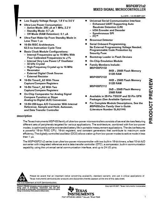
The Texas Instruments MSP430 family of ultralow power microcontrollers consist of several devices featuring different sets of peripherals targeted for various applications. The architecture, combined with five low power modes is optimized to achieve extended battery life in portable measurement applications. The device features a powerful 16-bit RISC CPU, 16-bit registers, and constant generators that attribute to maximum code efficiency. The digitally controlled oscillator (DCO) allows wake-up from low-power modes to active mode in less than 1μs. The MSP430x21x1 series is an ultralow-power mixed signal microcontroller with a built-in 16-bit timer, versatile analog comparator and sixteen I/O pins. Typical applications include sensor systems that capture analog signals, convert them to digital values, and then process the data for display or for transmission to a host system. Stand alone RF sensor front end is another area of application. The analog comparator provides slope A/D conversion capability.
device pinout
DW, PW, or DGV PACKAGE (TOP VIEW) TEST VCC P2.5/CA5 VSS XOUT/P2.7/CA7 XIN/P2.6/CA6 RST/NMI P2.0/ACLK/CA2 P2.1/INCLK/CA3 P2.2/CAOUT/TA0/CA4 1 2 3 4 5 6 7 8 9 10 20 19 18 17 16 15 14 13 12 11 P1.7/TA2/TDO/TDI P1.6/TA1/TDI/TCLK P1.5/TA0/TMS P1.4/SMCLK/TCK P1.3/TA2 P1.2/TA1 P1.1/TA0 P1.0/TACLK P2.4/TA2/CA1 P2.3/TA1/CA0 NC VSS XOUT/P2.7/CA7 XIN/P2.6/CA6 RST/NMI P2.0/ACLK/CA2 1 2 3 4 5 6 7 8 P2.2/CAOUT/TA0/CA4 P2.1/INCLK/CA3 9 10 11 12 P2.3/TA1/CA0 P2.4/TA2/CA1 NC NC P2.5/CA5 RGE PACKAGE (TOP VIEW) VCC TEST P1.7/TA2/TDO/TDI P1.6/TA1/TDI/TCLK
D Serial Onboard Programming,
No External Programming Voltage Needed Programmable Code Protection by Security Fuse Bootstrap Loader On Chip Emulation Module Family Members Include: MSP430F2101: 1KB + 256B Flash Memory 128B RAM MSP430F2111: 2KB + 256B Flash Memory 128B RAM MSP430F2121: 4KB + 256B Flash Memory 256B RAM MSP430F2131: 8KB + 256B Flash Memory 256B RAM Available in a 20-Pin Plastic Small-Outline Wide Body (SOWB) Package, 20-Pin Plastic Small-Outline Thin (TSSOP) Package, 20-Pin TVSOP and 24-Pin QFN For Complete Module Descriptions, Refer to the MSP430x2xx Family User’s Guide
MSP430x21x1 MIXED SIGNAL MICROCONTROLLER
SLAS439C − SEPTEMBER 2004 − REVISED JULY 2006
D Low Supply Voltage Range 1.8 V to 3.6 V D Ultralow-Power Consumption
Copyright © 2004 − 2006 Texas Instruments Incorporated
POST OFFICE BOX 655303
• DALLAS, TEXAS 75265
1
MSP430x21x1 MIXED SIGNAL MICROCONTROLLER
SLAS439C − SEPTEMBER 2004 − REVISED JULY 2006
PRODUCTION DATA information is current as of publication date. Products conform to specifications per the terms of Texas Instruments standard warranty. Production processing does not necessarily include testing of all parameters.
RST/NMI
NOTE: See port schematics section for detailed I/O information.
POST OFFICE BOX 655303
• DALLAS, TEXAS 75265
MSP430x21x1 MIXED SIGNAL MICROCONTROLLER
Basic Clock System+
MCLK
16MHz CPU incl. 16 Registers
MAB
MDB
Emulation (2BP) JTAG Interface Brownout Protection Watchdog WDT+ 15/16− Bit Timer_A3 3 CC Registers
functional block diagram
VCC VSS P1.x & JTAG 8 XIN XOUT ACLK SMCLK Flash 8kB 4kB 2kB 1kB RAM 256B 256B 128B 128B Port P1 Comparator _A+ 8 Channel Input Mux 8 I/O Interrupt capability, pull− up/down resistors Port P2 8 I/O Interrupt capability, pull− up/down resistors P2.x & XIN/XOUT 8
24 23 22 21 20 19
NC 18 P1.5/TA0/TMS 17 P1.4/SMCLK/TCK 16 P1.3/TA2 15 P1.2/TA1 14 P1.1/TA0 13 P1.0/TACLK
Note: NC pins not internally connected Power Pad connection to VSS recommended
D D D
D Basic Clock Module Configurations:
D
D D D
D
description
The Texas Instruments MSP430 family of ultralow power microcontrollers consist of several devices featuring different sets of peripherals targeted for various applications. The architecture, combined with five low power modes is optimized to achieve extended battery life in portable measurement applications. The device features a powerful 16-bit RISC CPU, 16-bit registers, and constant generators that attribute to maximum code efficiency. The digitally controlled oscillator (DCO) allows wake-up from low-power modes to active mode in less than 1μs. The MSP430x21x1 series is an ultralow-power mixed signal microcontroller with a built-in 16-bit timer, versatile analog comparator and sixteen I/O pins. Typical applications include sensor systems that capture analog signals, convert them to digital values, and then process the data for display or for transmission to a host system. Stand alone RF sensor front end is another area of application. The analog comparator provides slope A/D conversion capability.
device pinout
DW, PW, or DGV PACKAGE (TOP VIEW) TEST VCC P2.5/CA5 VSS XOUT/P2.7/CA7 XIN/P2.6/CA6 RST/NMI P2.0/ACLK/CA2 P2.1/INCLK/CA3 P2.2/CAOUT/TA0/CA4 1 2 3 4 5 6 7 8 9 10 20 19 18 17 16 15 14 13 12 11 P1.7/TA2/TDO/TDI P1.6/TA1/TDI/TCLK P1.5/TA0/TMS P1.4/SMCLK/TCK P1.3/TA2 P1.2/TA1 P1.1/TA0 P1.0/TACLK P2.4/TA2/CA1 P2.3/TA1/CA0 NC VSS XOUT/P2.7/CA7 XIN/P2.6/CA6 RST/NMI P2.0/ACLK/CA2 1 2 3 4 5 6 7 8 P2.2/CAOUT/TA0/CA4 P2.1/INCLK/CA3 9 10 11 12 P2.3/TA1/CA0 P2.4/TA2/CA1 NC NC P2.5/CA5 RGE PACKAGE (TOP VIEW) VCC TEST P1.7/TA2/TDO/TDI P1.6/TA1/TDI/TCLK
D Serial Onboard Programming,
No External Programming Voltage Needed Programmable Code Protection by Security Fuse Bootstrap Loader On Chip Emulation Module Family Members Include: MSP430F2101: 1KB + 256B Flash Memory 128B RAM MSP430F2111: 2KB + 256B Flash Memory 128B RAM MSP430F2121: 4KB + 256B Flash Memory 256B RAM MSP430F2131: 8KB + 256B Flash Memory 256B RAM Available in a 20-Pin Plastic Small-Outline Wide Body (SOWB) Package, 20-Pin Plastic Small-Outline Thin (TSSOP) Package, 20-Pin TVSOP and 24-Pin QFN For Complete Module Descriptions, Refer to the MSP430x2xx Family User’s Guide
MSP430x21x1 MIXED SIGNAL MICROCONTROLLER
SLAS439C − SEPTEMBER 2004 − REVISED JULY 2006
D Low Supply Voltage Range 1.8 V to 3.6 V D Ultralow-Power Consumption
Copyright © 2004 − 2006 Texas Instruments Incorporated
POST OFFICE BOX 655303
• DALLAS, TEXAS 75265
1
MSP430x21x1 MIXED SIGNAL MICROCONTROLLER
SLAS439C − SEPTEMBER 2004 − REVISED JULY 2006
PRODUCTION DATA information is current as of publication date. Products conform to specifications per the terms of Texas Instruments standard warranty. Production processing does not necessarily include testing of all parameters.