
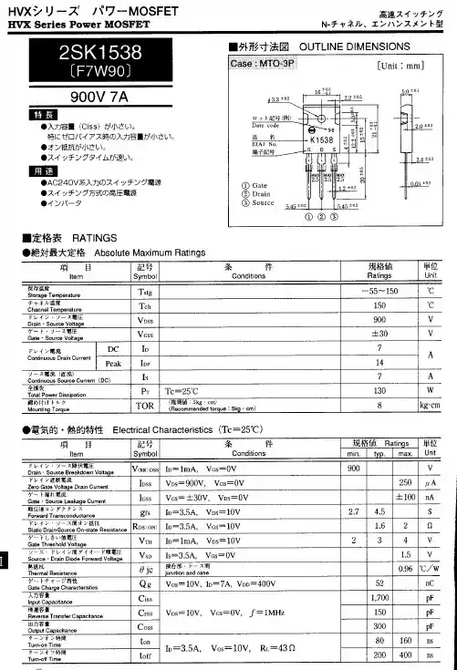
2SK1538-芯片资料介绍
- 格式:pdf
- 大小:152.89 KB
- 文档页数:2
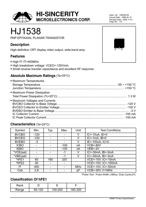
Page No. : 1/3HJ1538PNP EPITAXIAL PLANAR TRANSISTORDescriptionHigh-definition CRT display video output, wide-band amp.Features• High fT: fT=400MHz• High breakdown voltage: VCEO=-120Vmin• Small reverse transfer capacitance and excellent HF responseAbsolute Maximum Ratings (Ta=25°C)• Maximum TemperaturesStorage Temperature............................................................................................ -55 ~ +150 °C Junction Temperature.................................................................................................... +150 °C • Maximum Power DissipationTotal Power Dissipation (Tc=25°C)................................................................................... 1.3 W • Maximum Voltages and CurrentsBVCBO Collector to Base Voltage................................................................................... -120 V BVCEO Collector to Emitter Voltage................................................................................ -120 V BVEBO Emitter to Base Voltage.......................................................................................... -3 V IC Collector Current...................................................................................................... -100 mA IC Peak Collector Current............................................................................................. -100 mA Characteristics (Ta=25°C)Symbol Min.Typ.Max.Unit Test ConditionsBVCBO-120--V IC=-10uA, IE=0BVCEO-120--V IC=-1mA, IB=0BVEBO-3--V IE=-100uA, IC=0ICBO---100nA VCB=-80VIEBO---100nA VEB=-2V*VCE(sat)---1V IC=-30mA, IB=-3mA*VBE(sat)---1V IC=-30mA, IB=-3mA*hFE160160320VCE=-10V, IC=-10mA*hFE240--VCE=-10V, IC=-100mAfT400--MHz VCE=-10V, IC=-50mACob 2.8--pF VCB=-30V, f=1MHz*Pulse Test : Pulse Width ≤380us, Duty Cycle≤2% Classification Of hFE1Rank D E FRange60-120100-200160-320Page No. : 2/3 Characteristics CurvePage No. : 3/3*:TypicalInches Millimeters Inches Millimeters DIM Min.Max.Min.Max.DIM Min.Max.Min.Max.A 0.01770.02170.450.55G0.08660.1102 2.20 2.80B 0.06500.0768 1.65 1.95H -*0.0906-*2.30C 0.03540.05910.90 1.50I -0.0354-0.90D 0.01770.02360.450.60J -0.0315-0.80E 0.25200.2677 6.40 6.80K 0.20470.2165 5.20 5.50F0.21250.2283 5.40 5.80L0.05510.0630 1.40 1.60Notes : 1.Dimension and tolerance based on our Spec. dated May. 05,1996.2.Controlling dimension : millimeters.3.Maximum lead thickness includes lead finish thickness, and minimum lead thickness is the minimum thickness of base material.4.If there is any question with packing specification or packing method, please contact your local HSMC sales office.Material :• Lead : 42 Alloy ; solder plating• Mold Compound : Epoxy resin family, flammability solid burning class:UL94V-0Important Notice:• All rights are reserved. Reproduction in whole or in part is prohibited without the prior written approval of HSMC.• HSMC reserves the right to make changes to its products without notice.• HSMC semiconductor products are not warranted to be suitable for use in Life-Support Applications, or systems.• HSMC assumes no liability for any consequence of customer product design, infringement of patents, or application assistance.Head Office And Factory :• Head Office (Hi-Sincerity Microelectronics Corp.) : 10F.,No. 61, Sec. 2, Chung-Shan N. Rd. Taipei Taiwan R.O.C.Tel : 886-2-25212056 Fax : 886-2-25632712, 25368454• Factory 1 : No. 38, Kuang Fu S. Rd., Fu-Kou Hsin-Chu Industrial Park Hsin-Chu Taiwan. R.O.C Tel : 886-3-5983621~5 Fax : 886-3-5982931• Factory 2 : No. 17-1, Ta-Tung Rd., Fu-Kou Hsin-Chu Industrial Park Hsin-Chu Taiwan. R.O.C Tel : 886-3-5977061 Fax : 886-3-5979220。

TOSHIBA Field Effect Transistor Silicon N Channel MOS Type2SK3078AVHF/UHF Band Amplifier Applications· Output power: P o ≥ 28.0dBmW · Gain: G p ≥ 8.0dB· Drain Efficiency: ηD ≥ 50%Maximum Ratings (Ta = 25°C)Characteristics Symbol Rating UnitDrain-source voltage V DSS10 VGate-source voltage V GSS 5 V Drain current I D 0.5 A Power dissipation P D (Note 1)3WChannel temperature T ch 150 °C Storage temperature rangeT stg−45~150 °CNote 1: Tc = 25°CMarkingElectrical Characteristics (Ta = 25°C)Characteristics Symbol Test Condition Min Typ. Max UnitOutput power P O 28.0 ¾ ¾ dBmW Drain efficiency ηD 50 ¾ ¾ % Power gain G p V DS = 4.5 V, Iidle = 50 mA(V GS = adjust)f = 470 MHz, P i = 20dBmWZ G = Z L == 50 Ω 8.0 ¾ ¾ dB Threshold voltage V th V DS = 4.8 V, I D = 0.5 mA 0.20 ¾ 1.20VDrain cut-off current I DSS V DS = 10 V, V GS = 0 V ¾ ¾ 10 µA Gate-source leakage currentI GSSV GS = 5 V, V DS = 0 V¾¾ 5 µALoad mismatch (Note 2)¾V DS = 6.5 V, f = 470 MHz, P i = 20dBmW,P o = 28.0dBmW (V GS = adjust) VSWR LOAD 10:1 all phaseNo degradation ¾Caution: This transistor is the electrostatic sensitive device. Please handle with caution. Note 2: When the RF output power test fixture is usedUnit: mmJEDEC―JEITA SC-62 TOSHIBA 2-5K1DU WPF Output Power Test FixtureGS DSL1: f 0.6, 5.5ID, 5T L2: f 0.6, 5.5ID, 7TLine: 2 mmP i – P o , G p , EffIidle – G p , EffP i – P oP i – IddVdd – G p , EffP i – P oP i (dBmW)Iidle (mA)P i (dBmW)P i (dBmW)Vdd (V)P i (dBmW)G p (d B m W )P o (d B m W )D r a i n c u r r e n t (m A )P o (d B m W )E f f (%) P o (d B m W )G p (d B )E f f (%)10050Idd (%)255 15 20 10 03020100 302010 082 46Eff3020Vdd Vdd Vdd VddCaution: These are typical curves and devices are not necessarily guaranteed at these curves.P i – IddP i (dBmW)I d d (m A )301020· TOSHIBA is continually working to improve the quality and reliability of its products. Nevertheless, semiconductor devices in general can malfunction or fail due to their inherent electrical sensitivity and vulnerability to physical stress. It is the responsibility of the buyer, when utilizing TOSHIBA products, to comply with the standards of safety in making a safe design for the entire system, and to avoid situations in which a malfunction or failure of such TOSHIBA products could cause loss of human life, bodily injury or damage to property.In developing your designs, please ensure that TOSHIBA products are used within specified operating ranges as set forth in the most recent TOSHIBA products specifications. Also, please keep in mind the precautions and conditions set forth in the “Handling Guide for Semiconductor Devices,” or “TOSHIBA Semiconductor Reliability Handbook” etc.. · The TOSHIBA products listed in this document are intended for usage in general electronics applications (computer, personal equipment, office equipment, measuring equipment, industrial robotics, domestic appliances, etc.). These TOSHIBA products are neither intended nor warranted for usage in equipment that requires extraordinarily high quality and/or reliability or a malfunction or failure of which may cause loss of human life or bodily injury (“Unintended Usage”). Unintended Usage include atomic energy control instruments, airplane or spaceship instruments, transportation instruments, traffic signal instruments, combustion control instruments, medical instruments, all types of safety devices, etc.. Unintended Usage of TOSHIBA products listed in this document shall be made at the customer’s own risk. · The information contained herein is presented only as a guide for the applications of our products. No responsibility is assumed by TOSHIBA CORPORATION for any infringements of intellectual property or other rights of the third parties which may result from its use. No license is granted by implication or otherwise under any intellectual property or other rights of TOSHIBA CORPORATION or others. · The information contained herein is subject to change without notice.000707EAARESTRICTIONS ON PRODUCT USE。

123Request for your special attention and precautions in using the technical information andsemiconductors described in this book(1)If any of the products or technical information described in this book is to be exported or provided to non-residents, the laws andregulations of the exporting country, especially, those with regard to security export control, must be observed. (2)The technical information described in this book is intended only to show the main characteristics and application circuit examplesof the products, and no license is granted under any intellectual property right or other right owned by our company or any other company. Therefore, no responsibility is assumed by our company as to the infringement upon any such right owned by any other company which may arise as a result of the use of technical information described in this book.(3)The products described in this book are intended to be used for standard applications or general electronic equipment (such as officeequipment, communications equipment, measuring instruments and household appliances). Consult our sales staff in advance for information on the following applications:– Special applications (such as for airplanes, aerospace, automobiles, traffic control equipment, combustion equipment, life support systems and safety devices) in which exceptional quality and reliability are required, or if the failure or malfunction of the prod-ucts may directly jeopardize life or harm the human body.– Any applications other than the standard applications intended.(4)The products and product specifications described in this book are subject to change without notice for modification and/or im-provement. At the final stage of your design, purchasing, or use of the products, therefore, ask for the most up-to-date Product Standards in advance to make sure that the latest specifications satisfy your requirements. (5)When designing your equipment, comply with the range of absolute maximum rating and the guaranteed operating conditions(operating power supply voltage and operating environment etc.). Especially, please be careful not to exceed the range of absolute maximum rating on the transient state, such as power-on, power-off and mode-switching. Otherwise, we will not be liable for any defect which may arise later in your equipment.Even when the products are used within the guaranteed values, take into the consideration of incidence of break down and failure mode, possible to occur to semiconductor products. Measures on the systems such as redundant design, arresting the spread of fire or preventing glitch are recommended in order to prevent physical injury, fire, social damages, for example, by using the products.(6)Comply with the instructions for use in order to prevent breakdown and characteristics change due to external factors (ESD, EOS,thermal stress and mechanical stress) at the time of handling, mounting or at customer's process. When using products for which damp-proof packing is required, satisfy the conditions, such as shelf life and the elapsed time since first opening the packages.(7)This book may be not reprinted or reproduced whether wholly or partially, without the prior written permission of MatsushitaElectric Industrial Co., Ltd.M a i n t e n a n D i s c o n t i n u eP le a s ev i s it f o l l o w i n g U R L a b o u t l a t e s t i n fo r mh t t p ://p a n a s o n i c .n e t /s c /e n。
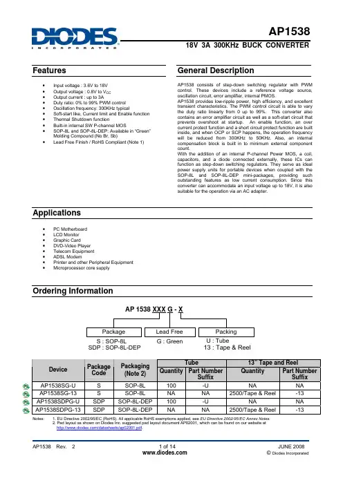
FeaturesGeneral DescriptionAP1538 consists of step-down switching regulator with PWM control. These devices include a reference voltage source, oscillation circuit, error amplifier, internal PMOS.• Input voltage : 3.6V to 18V • Output voltage : 0.8V to V CC • Output current : up to 3AAP1538 provides low-ripple power, high efficiency, and excellent transient characteristics. The PWM control circuit is able to vary the duty ratio linearly from 0 up to 99%. This converter also contains an error amplifier circuit as well as a soft-start circuit that prevents overshoot at startup. An enable function, an over current protect function and a short circuit protect function are built inside, and when OCP or SCP happens, the operation frequency will be reduced from 300KHz to 50KHz. Also, an internal compensation block is built in to minimum external component count.• Duty ratio: 0% to 99% PWM control • Oscillation frequency: 300KHz typical• Soft-start like, Current limit and Enable function • Thermal Shutdown function• Built-in internal SW P-channel MOS• SOP-8L and SOP-8L-DEP: Available in “Green” Molding Compound (No Br, Sb)•Lead Free Finish / RoHS Compliant (Note 1)With the addition of an internal P-channel Power MOS, a coil, capacitors, and a diode connected externally, these ICs can function as step-down switching regulators. They serve as ideal power supply units for portable devices when coupled with the SOP-8L and SOP-8L-DEP mini-packages, providing such outstanding features as low current consumption. Since this converter can accommodate an input voltage up to 18V, it is also suitable for the operation via an AC adapter.Applications• PC Motherboard • LCD Monitor • Graphic Card• DVD-Video Player • Telecom Equipment • ADSL Modem• Printer and other Peripheral Equipment •Microprocessor core supplyOrdering InformationAP 1538 XXX G - XPackage Packing S : SOP-8LLead Free U : Tube13 : Tape & ReelG : GreenSDP : SOP-8L-DEPTube 13” Tape and ReelDevice PackageCodePackaging (Note 2)Quantity Part Number Suffix Quantity Part NumberSuffixAP1538SG-U S SOP-8L 100 -U NA NA AP1538SG-13 S SOP-8L NA NA 2500/Tape & Reel -13 AP1538SDPG-U SDP SOP-8L-DEP 100 -U NA NA AP1538SDPG-13 SDP SOP-8L-DEP NA NA 2500/Tape & Reel -13Notes: 1. EU Directive 2002/95/EC (RoHS). All applicable RoHS exemptions applied, see EU Directive 2002/95/EC Annex Notes .2. Pad layout as shown on Diodes Inc. suggested pad layout document AP02001, which can be found on our website at/datasheets/ap02001.pdf .Pin Assignments(1) SOP-8L (2) SOP-8L-DEP (Dual Exposed Pads)FBOutputOCSETOutputENVssVssV CC( Top View )FBOutputOCSETOutputENVssVssV CC( Top View )Notes: 3. Exposed pad 1 is connected to VSS and exposed pad 2 is connected to Output. The board layout for exposed pads needs to be considered to avoid short circuit.Pin DescriptionsPin Name Pin No. DescriptionFB 1FeedbackpinEN 2Power-off pinH: Normal operation(Step-down operation)L: Step-down operation stopped(All circuits deactivated)OCSET 3 Add an external resistor to set max output currentV CC 4 IC power supply pinOutput 5,6Switch Pin. Connect external inductor/diode here. Minimize tracearea at this pin to reduce EMIV SS7, 8 GND PinBlock DiagramVccAbsolute Maximum RatingsSymbol ParameterRating Unit ESD HBM Human Body Model ESD Protection7 KV ESD MM Machine Model ESD Protection 450V V CC V CC Pin Voltage V SS - 0.3 to V SS + 20VV FB Feedback Pin Voltage V SS - 0.3 to V CC V V EN EN Pin Voltage V SS - 0.3 to V CC V V OUT Switch Pin Voltage V SS - 0.3 to V CC V P D Power DissipationInternally limited mWT J Operating Junction Temperature Range -40 to +125 o C T ST Storage Temperature Range-65 to +150oCCaution: The absolute maximum ratings are rated values exceeding which the product could suffer physical damage.These values must therefore not be exceeded under any conditions.Recommended Operating ConditionsSymbol Parameter MinMax Unit V IN Input Voltage (Note 4) 3.618VI OUT Output Current 0 3 A T A Operating Ambient Temperature-20+85o CNotes: 4. For the operations in low input voltage, AP1538 can tolerate down to 3.6V but max output current loading will be less than 3A. For nominalapplications in such low input voltage range, especially lower than 4V, a higher ROCSET with larger heat sink is recommended.Electrical Characteristics(V IN = 12V, T A = 25°C, unless otherwise specified) Symbol Parameter Conditions Min Typ. Max Unit V FB Feedback Voltage I OUT = 0.1A 0.784 0.8 0.816V I FB Feedback Bias Current I OUT = 0.1A- 0.1 0.5 µA I SHDN Current Consumption DuringPower Off V EN = 0V- 10 - µA ∆V OUT/ V INLine RegulationV IN = 5V~18V-12%∆V OUT/ V OUTLoad Regulation I OUT = 0.1 to 3A - 0.2 0.5 %f OSC Oscillation Frequency Measure waveform at SW pin 240 300 400 KHzf OSC1 Frequency of Current Limit orShort Circuit Protection Measure waveform at SW pin - 50 - KHzV IH Evaluate oscillation at SW pin 2.0 - -V IL EN Pin Input Voltage Evaluate oscillation stop at SW pin - - 0.8 V I SH EN Pin High - 20 - µAI SL EN Pin Input Leakage Current EN Pin Low - -10 - µA I OCSET OCSET Pin Bias Current -- 75 90 105 µAV IN =5V, V FB =0V - 110 -R DS(ON) Internal MOSFET R DS(ON)V IN =12V, V FB =0V -70 - m Ω EFFI EfficiencyV IN =12V, V OUT = 5VI OUT =3A- 92 - % T SHDN Thermal shutdown threshold - 150 - °C T HYS Thermal shutdown hysteresis - 55 - °CSOP-8L (Note 5) 24 θJC Thermal Resistance Junction-to-Case SOP-8L-DEP (Note 5) - 26- oC/WNotes: 5. Test condition for SOP-8L and SOP-8L-DEP: Devices mounted on 2oz copper, minimum recommended pad layout on top & bottom layer with thermal vias, double sided FR-4 PCB.Typical Application CircuitVV OUT = V FB x (1+R A /R B )R B = 0.7K~5K ohmNotes: 6. Suggested DIODES Power Schottky P/N: B340 series or PDS340.7. Suggested C OUT for V OUT < 1V; 680μF.8. Typical feedback compensation (Cc): 5600pF.Typical Performance CharacteristicsTypical Performance Characteristics (Continued)V OUT Ripple(V IN = 12V, V OUT = 3.3V, I OUT = 0.1A)V OUT Ripple(V IN = 12V, V OUT = 3.3V, I OUT = 3.0A)Load Transient Response(V IN = 12V, V OUT = 3.3V, I OUT = 0.1~3A)Test CircuitFunctional DescriptionPWM ControlThe AP1538 is a DC/DC converter that employs pulse width modulation (PWM) scheme. Its pulse width varies in the range of 0% to 99%, based on the output current loading. The output ripple voltage caused by the PWM high frequency switching can easily be reduced through an output filter. Therefore, this converter provides a low ripple output supply over a broad range of input voltage & output current loadingUnder Voltage LockoutThe under voltage lockout circuit of the AP1538 assures that the high-side MOSFET driver remains in the off state whenever the supply voltage drops below 3.3V. Normal operation resumes once V CC rises above 3.5V.Current Limit ProtectionThe current limit threshold is set by external resistor R OCSET connected from V CC supply to OCSET pin. The internal sink current I OCSET (90uA typical) across this resistor sets the voltage at OCSET pin. When the PWM voltage is less than the voltage at OCSET, an over-current condition is triggered.The current limit threshold is given by the following equation:R I R I OCSET OCSET DS(ON)PEAK ×=×2I)(I I (MAX) OUT PEAKΔ+>where,INOUTS OUT V V L F V V I ××−=ΔINI PEAK is the output peak current; R DS (ON) is the MOSFET ON resistance; F S is the PWM frequency (300KHz typical). Also, the inductor value will affect the ripple current ΔI.The above equation is recommended for input voltage range of 5V to 18V. For input voltage lower than 5V or ambient temperature over 100°C, higher R OCSET is recommended.The recommended minimum R OCSET value is summarized below:V IN (V) V OUT(V) 5V 12V 18V 0.8 4.7K 3.0K 3.3K 1.0 5.6K 3.0K 3.9K 1.2 5.6K 3.0K 3.9K 1.8 5.6K 3.0K 3.9K 2.5 5.6K 3.0K 3.9K 3.3 5.6K 3.0K 3.9K 5.0 N/A 3.0K 4.7KInductor SelectionFor most designs, the operates with inductors of 22µH to 33µH. The inductor value can be derived from the following equation:()oscL ONOUT IN f I T V V L ×Δ×−=2Where ΔI L is inductor Ripple Current. Large value inductors lower ripple current and small value inductors result in high ripple current. Choose inductor ripple current approximately 15% of the maximum load current 3A, ∆I L =0.45A. The DC current rating of the inductor should be at least equal to the maximum load current plus half the ripple current to prevent core saturation (3A+0.225A).Input Capacitor SelectionThis capacitor should be located close to the IC using short leads and the voltage rating should be approximately 1.5 times the maximum input voltage. The RMS current rating requirement for the input capacitor of a buck regulator is approximately 1⁄2 the DC load current. A low ESR input capacitor sized for maximum RMS current must be used. A 470µF low ESR capacitor for most applications is sufficient.Output Capacitor SelectionThe output capacitor is required to filter the output voltage and provides regulator loop stability. The important capacitor parameters are the 100KHz Equivalent Series Resistance (ESR), the RMS ripples current rating, voltage rating and capacitance value. For the output capacitor, the ESR value is the most important parameter. The output ripple can be calculated from the following formula.ESR I V L RIPPLE ×Δ=The bulk capacitor’s ESR will determine the output ripple voltage and the initial voltage drop after a high slew-rate transient.An aluminum electrolytic capacitor's ESR value is related to the capacitance and its voltage rating. In most case, higher voltage electrolytic capacitors have lower ESR values. Most of the time, capacitors with much higher voltage ratings may be needed to provide the low ESR values required for low output ripple voltage.PCB Layout GuideIf you need low T C & T J or large PD (Power Dissipation), The dual SW pins(5& 6) and Vss pins(7& 8)on the SOP-8L package are internally connected to die pad, The evaluation board should be allowed for maximum copper area at output (SW) pins.1. Connect FB circuits (R 1, R 2, C 1) as closely as possible and keep away from inductor flux for pure V FB .2. Connect C3 to Vcc and Vss pin as closely as possible to get good power filter effect.3. Connect R4 to Vcc and OCSET pin as closely as possible.4. Connect ground side of the C2 & D1 & C4 as closely as possible and use ground plane for best performance.Functional Description (Continued)Functional Description (Continued)V OUTVINFigure: Layout numbering comparison.Marking Information(1) SOP-8L( Top View )SOP-8LAP1538Logo Part No Year : "07" =2007 "08" =2008Xth week:01~52~G : Green(2) SOP-8L-DEP( Top View )SOP-8L-DEPLogo Part No Internal code Year : "07" =2007 "08" =2008Xth week:01~52~G : GreenE : SOP-8L-DEPPackage Information ( All Dimensions in mm ) (1) SOP-8LDetail "A"(Unit: mm)(2) SOP-8L-DEPBottom viewIMPORTANT NOTICEDiodes Incorporated and its subsidiaries reserve the right to make modifications, enhancements, improvements, corrections or other changes without further notice to any product herein. Diodes Incorporated does not assume any liability arising out of the application or use of any product described herein; neither does it convey any license under its patent rights, nor the rights of others. The user of products in such applications shall assume all risks of such use and will agree to hold Diodes Incorporated and all the companies whose products are represented on our website, harmless against all damages.LIFE SUPPORTDiodes Incorporated products are not authorized for use as critical components in life support devices or systems without the expressed written approval of the President of Diodes Incorporated.。