
39-01-2125;中文规格书,Datasheet资料
- 格式:pdf
- 大小:254.41 KB
- 文档页数:3

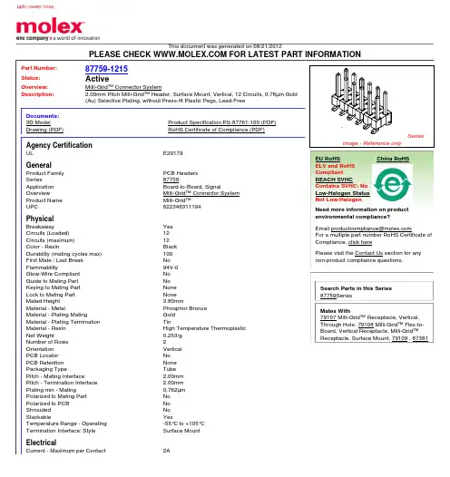
This document was generated on 08/21/2012PLEASE CHECK FOR LATEST PART INFORMATIONPart Number:87759-1215Status:ActiveOverview:Milli-Grid™ Connector SystemDescription:2.00mm Pitch Milli-Grid™ Header, Surface Mount, Vertical, 12 Circuits, 0.76µm Gold (Au) Selective Plating, without Press-fit Plastic Pegs, Lead-FreeDocuments:3D ModelProduct Specification PS-87761-100 (PDF)Drawing (PDF)RoHS Certificate of Compliance (PDF)Agency CertificationULE29179GeneralProduct Family PCB Headers Series87759Application Board-to-Board, SignalOverviewMilli-Grid™ Connector System Product Name Milli-Grid™UPC822348311194PhysicalBreakawayYes Circuits (Loaded)12Circuits (maximum)12Color - ResinBlack Durability (mating cycles max)100First Mate / Last Break No Flammability94V-0Glow-Wire Compliant No Guide to Mating Part No Keying to Mating Part None Lock to Mating Part None Mated Height 3.80mmMaterial - MetalPhosphor Bronze Material - Plating MatingGold Material - Plating Termination TinMaterial - Resin High Temperature Thermoplastic Net Weight0.253/g Number of Rows 2Orientation Vertical PCB Locator No PCB Retention None Packaging TypeTube Pitch - Mating Interface2.00mm Pitch - Termination Interface 2.00mm Plating min - Mating 0.762µm Polarized to Mating Part No Polarized to PCB No Shrouded No StackableYesTemperature Range - Operating -55°C to +105°C Termination Interface: StyleSurface Mount ElectricalCurrent - Maximum per Contact2ASeriesimage - Reference onlyEU RoHSChina RoHSELV and RoHS Compliant REACH SVHCContains SVHC: No Low-Halogen Status Not Low-HalogenNeed more information on product environmental compliance?Email productcompliance@For a multiple part number RoHS Certificate of Compliance, click herePlease visit the Contact Us section for any non-product compliance questions.Search Parts in this Series 87759SeriesMates With79107 Milli-Grid™ Receptacle, Vertical,Through Hole, 79108 Milli-Grid™ Flex-to-Board, Vertical Receptacle, Milli-Grid™Receptacle, Surface Mount, 79109 , 87381Voltage - Maximum125VSolder Process DataDuration at Max. Process Temperature (seconds)10Lead-free Process Capability Reflow Capable (SMT only)Max. Cycles at Max. Process Temperature3Process Temperature max. C260Material InfoReference - Drawing NumbersProduct Specification PS-87761-100Sales Drawing SD-87759-118This document was generated on 08/21/2012PLEASE CHECK FOR LATEST PART INFORMATION分销商库存信息: MOLEX 0877591215。
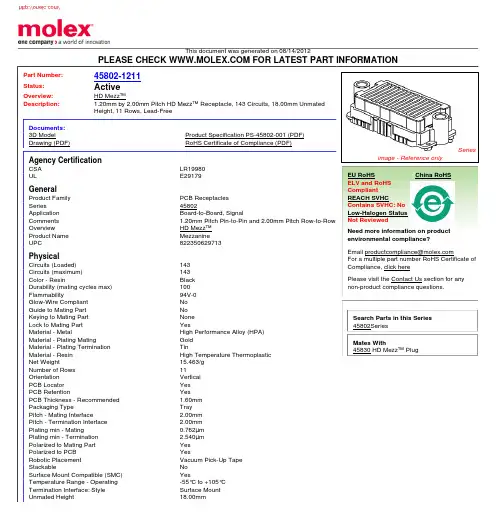
This document was generated on 08/14/2012PLEASE CHECK FOR LATEST PART INFORMATIONPart Number:45802-1211Status:ActiveOverview:HD Mezz™Description:1.20mm by2.00mm Pitch HD Mezz™ Receptacle, 143 Circuits, 18.00mm Unmated Height, 11 Rows, Lead-FreeDocuments:3D ModelProduct Specification PS-45802-001 (PDF)Drawing (PDF)RoHS Certificate of Compliance (PDF)Agency CertificationCSA LR19980ULE29179GeneralProduct Family PCB Receptacles Series45802Application Board-to-Board, SignalComments 1.20mm Pitch Pin-to-Pin and 2.00mm Pitch Row-to-Row OverviewHD Mezz™Product Name Mezzanine UPC822350629713PhysicalCircuits (Loaded)143Circuits (maximum)143Color - ResinBlack Durability (mating cycles max)100Flammability94V-0Glow-Wire Compliant No Guide to Mating Part No Keying to Mating Part None Lock to Mating Part YesMaterial - MetalHigh Performance Alloy (HPA)Material - Plating MatingGold Material - Plating Termination TinMaterial - Resin High Temperature Thermoplastic Net Weight15.463/g Number of Rows 11Orientation Vertical PCB Locator Yes PCB RetentionYes PCB Thickness - Recommended 1.60mm Packaging TypeTray Pitch - Mating Interface2.00mm Pitch - Termination Interface 2.00mm Plating min - Mating0.762µm Plating min - Termination 2.540µm Polarized to Mating Part Yes Polarized to PCB YesRobotic Placement Vacuum Pick-Up Tape StackableNo Surface Mount Compatible (SMC)YesTemperature Range - Operating -55°C to +105°C Termination Interface: Style Surface Mount Unmated Height18.00mmSeriesimage - Reference onlyEU RoHSChina RoHSELV and RoHS Compliant REACH SVHCContains SVHC: No Low-Halogen Status Not ReviewedNeed more information on product environmental compliance?Email productcompliance@For a multiple part number RoHS Certificate of Compliance, click herePlease visit the Contact Us section for any non-product compliance questions.Search Parts in this Series 45802SeriesMates With45830 HD Mezz™ PlugElectricalCurrent - Maximum per Contact2AGrounding to PCB NoVoltage - Maximum250V ACSolder Process DataDuration at Max. Process Temperature (seconds)20Lead-free Process Capability Reflow Capable (SMT only)Max. Cycles at Max. Process Temperature2Process Temperature max. C260Material InfoReference - Drawing NumbersProduct Specification PS-45802-001Sales Drawing SD-45802-0001, SD-45802-0002This document was generated on 08/14/2012PLEASE CHECK FOR LATEST PART INFORMATION分销商库存信息: MOLEX 0458021211。

12-Bit RDCwith Reference OscillatorAD2S1205 Rev. AInformation furnished by Analog Devices is believed to be accurate and reliable. However, noresponsibility is assumed by Analog Devices for its use, nor for any infringements of patents or other rights of third parties that may result from its use. Specifications subject to change without notice. No license is granted by implication or otherwise under any patent or patent rights of Analog Devices. T rademarks and registered trademarks are the property of their respective owners. One Technology Way, P.O. Box 9106, Norwood, M A 02062-9106, U.S.A. Tel: 781.329.4700 Fax: 781.461.3113 ©2007–2010 Analog Devices, Inc. All rights reserved.FEATURESComplete monolithic resolver-to-digital converter (RDC) Parallel and serial 12-bit data portsSystem fault detection±11 arc minutes of accuracyInput signal range: 3.15 V p-p ± 27%Absolute position and velocity outputs1250 rps maximum tracking rate, 12-bit resolution Incremental encoder emulation (1024 pulses/rev) Programmable sinusoidal oscillator on boardSingle-supply operation (5.00 V ± 5%)−40°C to +125°C temperature rating44-lead LQFP4 kV ESD protectionQualified for automotive applications APPLICATIONSAutomotive motion sensing and controlHybrid-electric vehiclesElectric power steeringIntegrated starter generator/alternatorIndustrial motor controlProcess control FUNCTIONAL BLOCK DIAGRAMFigure 1.GENERAL DESCRIPTIONThe AD2S1205 is a complete 12-bit resolution tracking resolver-to-digital converter that contains an on-board programmable sinusoidal oscillator providing sine wave excitation for resolvers.The converter accepts 3.15 V p-p ± 27% input signals on the Sin and Cos inputs. A Type II tracking loop is employed to track the inputs and convert the input Sin and Cos information into a digital representation of the input angle and velocity. The maximum tracking rate is a function of the external clock frequency. The performance of the AD2S105 is specified across a frequency range of 8.192 MHz ± 25%, allowing a maximum tracking rate of 1250 rps. PRODUCT HIGHLIGHTS1.Ratiometric Tracking Conversion. The Type II trackingloop provides continuous output position data withoutconversion delay. It also provides noise immunity andtolerance of harmonic distortion on the reference andinput signals.2.System Fault Detection. A fault detection circuit can senseloss of resolver signals, out-of-range input signals, inputsignal mismatch, or loss of position tracking.3.Input Signal Range. The Sin and Cos inputs can acceptdifferential input voltages of 3.15 V p-p ± 27%.4.Programmable Excitation Frequency. Excitation frequencyis easily programmable to 10 kHz, 12 kHz, 15 kHz, or 20 kHz by using the frequency select pins (the FS1 and FS2 pins).5.Triple Format Position Data. Absolute 12-bit angular positiondata is accessed via either a 12-bit parallel port or a 3-wire serial interface. Incremental encoder emulation is in standard A-quad-B format with direction output available.6.Digital Velocity Output. 12-bit signed digital velocity accessedvia either a 12-bit parallel port or a 3-wire serial interface.AD2S1205Rev. A | Page 2 of 20TABLE OF CONTENTSFeatures .............................................................................................. 1 Applications ....................................................................................... 1 Functional Block Diagram .............................................................. 1 General Description ......................................................................... 1 Product Highlights ........................................................................... 1 Revision History ............................................................................... 2 Specifications ..................................................................................... 3 Absolute Maximum Ratings ............................................................ 5 ESD Caution .................................................................................. 5 Pin Configuration and Function Descriptions ............................. 6 Resolver Format Signals ................................................................... 8 Theory of Operation ........................................................................ 9 Fault Detection Circuit ................................................................ 9 Monitor Signal .............................................................................. 9 Loss of Signal Detection .............................................................. 9 Signal Degradation Detection .................................................. 10 Loss of Position Tracking Detection ........................................ 10 Responding to a Fault Condition ............................................. 10 False Null Condition .................................................................. 10 On-Board Programmable Sinusoidal Oscillator .................... 11 Synthetic Reference Generation ............................................... 11 Charge-Pump Output ................................................................ 11 Connecting the Converter ........................................................ 11 Clock Requirements ................................................................... 12 Absolute Position and Velocity Output ................................... 12 Parallel Interface ......................................................................... 12 Serial Interface ............................................................................ 14 Incremental Encoder Outputs .................................................. 16 Supply Sequencing and Reset ................................................... 16 Circuit Dynamics ........................................................................... 17 Loop Response Model ............................................................... 17 Sources of Error .......................................................................... 18 Connecting to the DSP .............................................................. 19 Outline Dimensions ....................................................................... 20 Ordering Guide .......................................................................... 20 Automotive Products .. (20)REVISION HISTORY5/10—Rev. 0 to Rev. AChanges to Features Section............................................................ 1 Changes to Input Bias Current Parameter and InputImpedance Parameter ...................................................................... 3 Changes to Table 2 ............................................................................ 5 Changes to Loss of Signal Detection Section ................................ 9 Changes to Connecting the Converter Section and Figure 5 ... 11 Change to t 6 Max Value in Table 6 ............................................... 13 Changes to t 9 and t 10 Max Values Table 7 .................................... 15 Changes to Ordering Guide .......................................................... 20 Added Automotive Products Section .......................................... 20 1/07—Revision 0: Initial VersionAD2S1205SPECIFICATIONSAV DD = DV DD = 5.0 V ± 5% at −40°C to +125°C, CLKIN = 8.192 MHz ± 25%, unless otherwise noted.Rev. A | Page 3 of 20AD2S12051 The voltages for Sin, SinLO, Cos, and CosLO relative to AGND must be between 0.2 V and AV DD.Rev. A | Page 4 of 20AD2S1205Rev. A | Page 5 of 20ABSOLUTE MAXIMUM RATINGSTable 2.Parameter RatingSupply Voltage (V DD ) −0.3 V to +7.0 VSupply Voltage (AV DD ) −0.3 V to +7.0 VInput Voltage −0.3 V to V DD + 0.3 VOutput Voltage Swing −0.3 V to V DD + 0.3 VInput Current to Any Pin Except Supplies 1 ±10 mAOperating Temperature Range (Ambient) −40°C to +125°C Storage Temperature Range −65°C to +150°C1Transient currents of up to 100 mA do not cause latch-up.Stresses above those listed under Absolute Maximum Ratings may cause permanent damage to the device. This is a stressrating only; functional operation of the device at these or anyother conditions above those indicated in the operationalsection of this specification is not implied. Exposure to absolutemaximum rating conditions for extended periods may affectdevice reliability. ESD CAUTIONAD2S1205Rev. A | Page 6 of 2006339-002PIN CONFIGURATION AND FUNCTION DESCRIPTIONSR E F O U T44R E F B Y P43C o s L O40S i n L O38A G N D42A G N D36A V D D39E X C35E X C34C o s41S i n37DV DD 1RD 2CS 3SAMPLE4RDVEL 5SOE 6DB11/SO 7DB10/SCLK8DB99DB810DB71133FS232FS131LOT 30DOS 29AD2S1205TOP VIEW (Not to Scale)DIR 28NM 27B 26A 25CPO 24DGND23DB 612D B 513D B 414D B 315D G N D16D V D D17D B 218D B 119D B 020X T A L O U T21C L K I N22Figure 2. Pin ConfigurationAD2S1205Rev. A | Page 7 of 20AD2S1205Rev. A | Page 8 of 20RESOLVER FORMAT SIGNALS06339-003V b = V s × Sin(ωt) × Sin(θ)(A) CLASSICAL RESOLVERs × Sin(ωt) × Cos(θ)V b = V s × Sin(ωt) × Sin(θ)(B)VARIABLE RELUCTANCE RESOLVERs × Sin(ωt) × Cos(θ)Figure 3. Classical Resolver vs. Variable Reluctance ResolverA classical resolver is a rotating transformer that typically has a primary winding on the rotor and two secondary windings on the stator. A variable reluctance resolver, on the other hand, has the primary and secondary windings on the stator and no windings on the rotor, as shown in Figure 3; however, the saliency in this rotor design provides the sinusoidal variation in the secondary coupling with the angular position. For both designs, the resolver output voltages (S3 − S1, S2 − S4) are as follows:Sinθt Sin E S1S30×ω=−)( (1)Cosθt Sin E S4S20×ω=−)(where:θ is the shaft angle.Sin(ωt) is the rotor excitation frequency. E 0 is the rotor excitation amplitude.The stator windings are displaced mechanically by 90° (see Figure 3). The primary winding is excited with an ac reference. The amplitude of subsequent coupling onto the secondary windings is a function of the position of the rotor (shaft) relative to the stator. The resolver therefore produces two output voltages (S3 − S1, S2 − S4), modulated by the sine and cosine of the shaft angle. Resolver format signals refer to the signals derived from the output of a resolver, as shown in Equation 1. Figure 4 illustrates the output format. 06339-0040°R2 – R4(REFERENCE)90°180°θ270°360°Figure 4. Electrical Resolver RepresentationAD2S1205Rev. A | Page 9 of 20THEORY OF OPERATIONThe AD2S1205’s operation is based on a Type II tracking closed-loop principle. The digitally implemented tracking loop continually tracks the position and velocity of the resolver without the need for external convert and wait states. As the resolver moves through a position equivalent to the least significant bit weighting, the tracking loop output is updated by 1 LSB.The converter tracks the shaft angle (θ) by producing an output angle (ϕ) that is fed back and compared with the input angle (θ); the difference between the two angles is the error, which is driven towards 0 when the converter is correctly tracking the input angle. T o measure the error, S3 − S1 is multiplied by Cosϕ and S2 − S4 is multiplied by Sinϕ to giveS4 S2for )(S1S3for )(00−×−×SinφCosθωt Sin E CosφSinθωt Sin E (2)The difference is taken, giving)()(0SinφCosθCos Sinθωt Sin E −φ× (3)This signal is demodulated using the internally generated synthetic reference, yielding)(0φ−φSin CosθCos SinθE (4)Equation 4 is equivalent to E 0Sin (θ − ϕ), which is approximately equal to E 0(θ − ϕ) for small values of θ − ϕ, where θ − ϕ is the angular error. The value E 0(θ − ϕ) is the difference between the angular error of the rotor and the digital angle output of the converter. A phase-sensitive demodulator, some integrators, and a compen-sation filter form a closed-loop system that seeks to null the error signal. If this is accomplished, ϕ equals the resolver angle, θ, within the rated accuracy of the converter. A Type II tracking loop is used so that constant velocity inputs can be tracked without inherent error.For more information about the operation of the converter, see the Circuit Dynamics section.FAULT DETECTION CIRCUITThe AD2S1205 fault detection circuit can sense loss of resolver signals, out-of-range input signals, input signal mismatch, or loss of position tracking; however, the position indicated by the AD2S1205 may differ significantly from the actual shaft position of the resolver.MONITOR SIGNALThe AD2S1205 generates a monitor signal by comparing the angle in the position register to the incoming Sin and Cos signals from the resolver. The monitor signal is created in a similar fashion to the error signal (described in the Theory of Operation section). The incoming Sinθ and Cosθ signals are multiplied by the Sin and Cos of the output angle, respectively, and then these values are added together:)()(CosφCosθA2SinφSinθA1Monitor ××+××= (5)where:A1 is the amplitude of the incoming Sin signal (A1 × Sinθ). A2 is the amplitude of the incoming Cos signal (A2 × Cosθ).θ is the resolver angle.ϕ is the angle stored in the position register.Note that Equation 5 is shown after demodulation with thecarrier signal Sin(ωt) removed. Also note that for a matchedinput signal (that is, a no fault condition), A1 is equal to A2.When A1 is equal to A2 and the converter is tracking (therefore, θ is equal to ϕ), the monitor signal output has aconstant magnitude of A1 (Monitor = A1 × (Sin 2θ + Cos 2θ) = A1), which is independent of the shaft angle. When A1 does notequal A2, the monitor signal magnitude alternates between A1 and A2 at twice the rate of the shaft rotation. The monitor signal is used to detect degradation or loss of input signals. LOSS OF SIGNAL DETECTIONLoss of signal (LOS) is detected when either resolver input (Sin or Cos) falls below the specified LOS Sin/Cos threshold. The AD2S1205 detects this by comparing the monitor signal to a fixed minimum value. Without the use of external circuitry, the AD2S1205 can detect the loss of up to three of the four connections from the resolver. The addition of two external 68 kΩ resistors, as outlined in Figure 5, ensures that the loss of all 4 connections, that is, complete removal of the resolver, may also be detected. LOS is indicated by both DOS and LOT latching as logic low outputs. The DOS and LOT pins are reset to the no fault state by a rising edge of SAMPLE . The LOS condition has priority over both the DOS and LOT conditions, as shown in . LOS is indicated within 57° of the angular output error (worst case).Table 4AD2S1205Rev. A | Page 10 of 20SIGNAL DEGRADATION DETECTIONDegradation of signal (DOS) is detected when either resolver input (Sin or Cos) exceeds the specified DOS Sin/Cos threshold. The AD2S1205 detects this by comparing the monitor signal to a fixed maximum value. In addition, DOS is detected when the amplitudes of the Sin and Cos input signals are mismatched by more than the specified DOS Sin/Cos mismatch. This is identified because the AD2S1205 continuously stores the minimum and maximum magnitude of the monitor signal in internal registers and calculates the difference between these values. DOS is indicated by a logic low on the DOS pin and is not latched when the input signals exceed the maximum input level. When DOS is indicated due to mismatched signals, the output is latched low until a rising edge of SAMPLE resets the stored minimum and maximum values. The DOS condition has priority over the LOT condition, as shown in . DOS is indicated within 33° of the angular output error (worst case).Table 4LOSS OF POSITION TRACKING DETECTIONLoss of tracking (LOT) is detected when • The internal error signal of the AD2S1205 exceeds 5°. • The input signal exceeds the maximum tracking rate. •The internal position (at the position integrator) differs from the external position (at the position register) by more than 5°.LOT is indicated by a logic low on the LOT pin and is not latched. LOT has a 4° hysteresis and is not cleared until the internal error signal or internal/external position mismatch is less than 1°. When the maximum tracking rate is exceeded, LOT is cleared only if the velocity is less than the maximum tracking rate and the internal/external position mismatch is less than 1°. LOT can be indicated for step changes in position (such as after a RESET signal is applied to the AD2S1205), or for accelerations of >~65,000 rps 2. It is also useful as a built-in test to indicate that the tracking converter is functioningproperly. The LOT condition has lower priority than both the DOS and LOS conditions, as shown in . The LOT and DOS conditions cannot be indicated at the same time. Table 4Table 4. Fault Detection DecodingConditionDOS Pin LOT Pin Order of Priority Loss of Signal (LOS)0 0 1 Degradation of Signal (DOS) 0 1 2 Loss of Tracking (LOT) 1 0 3 No Fault1 1RESPONDING TO A FAULT CONDITIONIf a fault condition (LOS, DOS, or LOT) is indicated by the AD2S1205, the output data is presumed to be invalid. Even if a RESET or SAMPLE pulse releases the fault condition and is not immediately followed by another fault, the output data may be corrupted. As discussed previously, there are some fault conditions with inherent latency. If the device fault is cleared, there may be some latency in the resolver’s mechanical position before the fault condition is reindicated.When a fault is indicated, all output pins still provide data, although the data may or may not be valid. The fault condition does not force the parallel, serial, or encoder outputs to a known state. Response to specific fault conditions is a system-level requirement. The fault outputs of the AD2S1205 indicate that the device has sensed a potential problem with either the internal or external signals of the AD2S1205. It is the responsibility of the system designer to implement the appropriate fault-handling schemes within the control hardware and/or algorithm of a given appli-cation based on the indicated fault(s) and the velocity or position data provided by the AD2S1205.FALSE NULL CONDITIONResolver-to-digital converters that employ Type II tracking loops based on the previously stated error equation (see Equation 4 in the Theory of Operation section) can suffer from a condition known as a false null. This condition is caused by a metastable solution to the error equation when θ − ϕ = 180°. The AD2S1205 is not susceptible to this condition because its hysteresis is implemented external to the tracking loop. As a result of the loop architecture chosen for the AD2S1205, the internal error signal constantly has some movement (1 LSB per clock cycle); therefore, in a metastable state, the converter moves to anunstable condition within one clock cycle. This causes the tracking loop to respond to the false null condition as if it were a 180° step change in input position (the response time is the same, as specified in the Dynamic Performance section of Table 1). Therefore, it is impossible to enter the metastable condition after the start-up sequence if the resolver signals are valid.分销商库存信息:ANALOG-DEVICESAD2S1205WSTZ AD2S1205YSTZ ADW71205WSTZ-RL ADW71205WSTZ ADW71205YSTZ EVAL-AD2S1205SDZ。

M I C R O J A C K S98density packaging•Beryllium Copper multi-spring contact maintains retention after multiple insertions•Ideal for mounting transistors,re-sistors,diodes,IC’s and similar miniature components•Custom micro jacks manufactured to your specifications •Other platings available upon request.016 [0.41].083[2.11].055[1.40]L3-FINGER CLOSED ENTRY CONTACT.038[0.96].038[0.96]HEX ..020[0.50].130 [3.3].095 [2.4]L.072[1.9].045[1.14]4-FINGER CLOSED ENTRY CONTACT.056[1.42].049[1.24].041[1.04].063[1.60]4-FINGER CLOSED ENTRY CONTACT.205[5.2].089[2.23].248[6.3]4-FINGER CLOSED ENTRY CONTACT.120[3.1].259[6.6].233[5.9].060[1.52]DIA..014[0.4].077[2.0]DIA..015(.38)-.021(.53)PIN -SOLDER MOUNT.015(.38)-.021(.53)PIN -PRESS FIT.015(.38)-.025(.64)PIN -TAPER-FIT.022(.56)-.032(.81)PIN -SOLDER MOUNT.015(.38)-.025(.64)PIN -SOLDER MOUNT.015(.38)-.025(.64)PIN -SOLDER MOUNT.022(.56)-.034(.86)PIN -PRESS FIT.025(.64)-.037(.94)PIN -PRESS FIT.025(.64)-.037(.94)PIN -SOLDER MOUNT.055[1.39].072[1.83].016 [0.41]4-FINGER CLOSED ENTRY CONTACT.093 [2.36].142[3.6].161[4.1]RoHS NON-RoHS Mtg.GOLD/GOLD TIN/TIN TIN/GOLD L Hole CAT.NO.CAT.NO.CAT.NO.Length Dia.1411-11431-11420-1.140(3.6).0421411-21431-21420-2.170(4.3)(1.07)RoHS NON-RoHS Mtg.GOLD/GOLD TIN/TIN TIN/GOLD L Hole CAT.NO.CAT.NO.CAT.NO.Length Dia.1412-11432-11468-1.140(3.6).0401412-21432-21468-2.170(4.3)(1.02)1412-31432-31468-3.282(7.2)RoHS NON-RoHS Mtg.GOLD/GOLD TIN/TIN TIN/GOLD L Hole CAT.NO.CAT.NO.CAT.NO.Length Dia.1415-11435-11469-1.160(4.1).0551415-21435-21469-2.190(4.8)(1.40)RoHS NON-RoHS Mtg.GOLD/GOLD TIN/TIN TIN/GOLD Hole CAT.NO.CAT.NO.CAT.NO.Dia.169316941695.063(1.60)RoHS NON-RoHS Mtg.GOLD/GOLD TIN/TIN TIN/GOLD Hole CAT.NO.CAT.NO.CAT.NO.Dia.141314331470.059(1.50)RoHS NON-RoHS Mtg.GOLD/GOLD TIN/TIN TIN/GOLD Hole CAT.NO.CAT.NO.CAT.NO.Dia.160316061607.052(1.32).061 [1.55].015[0.38].028[0.71].091 [2.3].086[2.2].170[4.3].200[5.1].070 [1.78]KNURL6-FINGER CLOSEDENTRY CONTACT6-FINGER CLOSED ENTRY CONTACT.057[1.45].077[1.96].083[2.11].025[0.7]L.025(.64)-.037(.94)PIN -SOLDER MOUNTRoHS NON-RoHS Mtg.GOLD/GOLD TIN/TIN TIN/GOLD Hole CAT.NO.CAT.NO.CAT.NO.Dia.141614361471.067(1.70)RoHSNON-RoHS Mtg.GOLD/GOLD TIN/TIN TIN/GOLD L Hole CAT.NO.CAT.NO.CAT.NO.Length Dia.1626-11614-11619-1.095(2.4).0621626-21614-21619-2.105(2.7)(1.57)1626-31614-31619-3.155(3.9).045 [1.14].062[1.57].090[2.29]6-FINGER CLOSED ENTRY CONTACT.080 [2.03].083 [2.11].022(.56)-.034(.86)PIN -SOLDER MOUNTRoHS NON-RoHS Mtg.GOLD/GOLD TIN/TIN TIN/GOLD Hole CAT.NO.CAT.NO.CAT.NO.Dia.165816591673.065(1.65).128[3.3].168[4.3].040 [1.02].092 [2.34].065 [1.65]L.200[5.1].230[5.9]4-FINGER CLOSED ENTRY CONTACT.125 [3.2].032(.81)-.046(1.17)PIN -SWAGE MOUNTRoHS NON-RoHS Mtg.GOLD/GOLD TIN/TIN TIN/GOLD Hole CAT.NO.CAT.NO.CAT.NO.Dia.359035913592.065(1.65)RoHS NON-RoHS Mtg.GOLD/GOLD TIN/TIN TIN/GOLD Hole CAT.NO.CAT.NO.CAT.NO.Dia.169716981699.063(1.60)RoHSNON-RoHS Mtg.GOLD/GOLD TIN/TIN TIN/GOLD L Hole CAT.NO.CAT.NO.CAT.NO.Length Dia.1419-11439-11478-1.062(1.6).0691419-21439-21478-2.094(2.4)(1.75)PLATING OPTIONSCONTACT PLATING BODY SPRING RoHS Gold/Gold Gold Gold Compliant Tin/Tin Tin/Lead Tin/Lead Non-CompliantTin/GoldTin/LeadGoldBody:Brass,ASTM-B16Spring:Beryllium Copper(QQ-C-533).057[1.45]HEX.057[1.45]DIA..200[5.1].020[0.52].078[1.98]DIA.6-FINGER CLOSED ENTRY CONTACT.165[4.2].078[1.98].040[1.02].090[2.29].040[1.02].062[1.57].210[5.3].187[4.7].180[4.6]6-FINGER CLOSED ENTRY CONTACTRoHS Plating:Gold:.000010per MIL-G-45204(RoHS Compliant)Tin/Lead:.000200to.000300per MIL-T-10727,Type 1(Non-RoHS Compliant).038[0.96]3-FINGER CLOSED ENTRY CONTACTL .055[1.40].083[2.11].016[0.41]RoHS Tel (718)956-8900•Fax (718)956-9040(800)221-5510•kec@31-0720th Road –Astoria,NY 11105-2017RoHS COMPLIANT ~ISO 9001CERTIFIED®分销商库存信息:KEYSTONE-ELECTRONICS1435-21431-11431-2 1420-11420-21470 1411-11411-21435-1 1469-11469-21614-3 1468-11468-21607 16951619-31606 169414711699 1415-11415-21413 359116981659 359216031432-1 1432-21432-31673 1468-316581697 1614-214161619-1 1619-216933590 1626-11626-21626-3 1412-11412-21412-3 1439-11439-21478-2 1419-21419-1。