脉宽调制技术外文翻译
- 格式:docx
- 大小:819.74 KB
- 文档页数:27
毕业设计外文资料翻译学院:专业:姓名:学号:外文出处: Home Power #75·February/March2000 (用外文写)24.437 Power Electronics附件: 1.外文资料翻译译文;2.外文原文。
附件1:外文资料翻译译文自制程序脉冲幅宽调节——应用于12-24伏G.弗勒斯特库克宽幅脉冲调节器(PWM)可以作为调光器使用,还可以作为直流电机调速器。
这里所描述的设备可以控制几安培的直流电流。
该电路系统可以用于调节12-24伏内的微小变化。
此设备已被用于控制汽车尾灯亮度,以及电脑电源控制的小型直流风扇的转速。
脉冲幅宽调节一个PWM电路的工作原理是形成一系列占空比率可控的直流脉冲方波。
在平均时间内可以有0-100%的不同变化。
这样,就能把量化的电力传送到负载。
PWM电路相比于电阻功率控制器上的的主要优点是效率更高。
在PWM的50%的水平时,将使用全部功率的50%,几乎将所有这些都转移到负载。
而在电阻功率控制器的50%水平时,将消耗约全部功率的71%;50%的功率转移到负载,另外21%的能量浪费到了加热电阻上。
根据负载电流,通常PWM电路浪费的功率远低于1%。
它需要在连续恒定功率下运行,所以更多被用于高功率负载的效率提高。
优势能源再生系统中的关键是提高负载效率。
一个脉宽调制器的另一个优点是,有充分的脉冲电源电压,并且产生一个更容易克服电机内阻的更大的扭矩。
而一个电阻功率控制器对电机速度的控制会使电压减弱,这将导致电机反应延迟。
最后,在PWM电路,常见的小电位器可用于控制各种负载,而大型和昂贵的高功率可变电阻器必须要用电阻控制器。
缺点脉宽调制电路的主要缺点是增加了复杂性,和可能产生射频干扰(RFI)。
射频干扰会更少通过附近的负载控制器而通过短路线,而且在某些情况下,会通过额外的电源滤波线路。
该电路会产生调幅无线干扰,这些干扰在横跨负载电容(C3)的旁路形成,远离最近的引脚。
外文原文Pulse-width modulationPulse-width modulation(PWM)is a modulationtechnique that conforms th ewidth of thepulse,formally the pulse duration,based on modulator signal informat ion。
Althoughthis modulation technique can be used to encode information for transmission,its mainuse is to allow the control of the power suppliedtoelectrical devices,especially to inertialloadssuch as motors.Inaddition,PWM is oneof the two principal algorithms used in photovoltaic solar battery chargers,[1]The averagevalue of voltage (and current)fed totheload iscontrolle dbyturning the switch betweensupply andload onand offatafa st pace。
The longer the switchisoncompared tothe off periods,the higher the powersupplied to the load is.ThePWM switching frequency has to bemuchfaster than whatwould affect the loa d,which is to say thedevice thatuses the power. Typically switchings have tobe done several times a minute in an electric stove,120 Hz inalamp dimmer,fromfewkilohertz(kHz)to tens of kHz foramotor drive and well into the tens or hundreds ofkHzin audioamplifiers and computer power supplies.The term duty cycledescribes theproportionof 'on’ time totheregular interval or ’period'of time; a low dutycyclecorresponds tolow power, because t he powerisofffor most ofthetime.Duty cycle is expressed in percent, 100% being fully on.Themain advantage ofPWM is thatpower loss in the switchingdevices is very low. Whenaswitch is off there is practically no current, andwhen it ison,there is almost no voltage dropacross the switch。
正弦波脉冲宽度调制英文缩写Sine Wave Pulse Width Modulation, often shortened as SPWM, is a technique used in power electronics to control the output voltage of an inverter or converter. It's pretty handy when you want to adjust the power delivery in a precise way.SPWM, as the name suggests, modulates the pulse width of a sine wave. This modulation is key to controlling the average voltage and, ultimately, the power output. It'slike having a dimmer switch for your electronic devices.The beauty of SPWM lies in its simplicity and effectiveness. By adjusting the pulse width, you can precisely manipulate the output voltage. This makes it perfect for applications where precise control is crucial, like in motor drives or renewable energy systems.In practical use, SPWM is implemented using digital controllers or specialized hardware. The result is a smoothand efficient power delivery, minimizing power losses and improving overall system performance.So in a nutshell, SPWM is a cool technique that lets you control the voltage output of electronic devices using sine wave pulses. It's efficient, precise, and pretty useful in a wide range of applications.。
脉冲宽度调制脉冲宽度调制(PWM)是英文“Pulse Width Modulation”的缩写,简称脉宽调制。
它是利用微处理器的数字输出来对模拟电路进行控制的一种非常有效的技术,广泛应用于测量,通信,功率控制与变换等许多领域。
一种模拟控制方式,根据相应载荷的变化来调制晶体管栅极或基极的偏置,来实现开关稳压电源输出晶体管或晶体管导通时间的改变,这种方式能使电源的输出电压在工作条件变化时保持恒定。
脉冲宽度调制(PWM)是一种对模拟信号电平进行数字编码的方法。
通过高分辨率计数器的使用,方波的占空比被调制用来对一个具体模拟信号的电平进行编码。
PWM信号仍然是数字的,因为在给定的任何时刻,满幅值的直流供电要么完全有(ON),要么完全无(OFF)。
电压或电流源是以一种通(ON)或断(OFF)的重复脉冲序列被加到模拟负载上去的。
通的时候即是直流供电被加到负载上的时候,断的时候即是供电被断开的时候。
只要带宽足够,任何模拟值都可以使用PWM进行编码。
多数负载(无论是电感性负载还是电容性负载)需要的调制频率高于10Hz,通常调制频率为1kHz到200kHz之间。
许多微控制器内部都包含有PWM控制器。
例如,Microchip公司的PIC16C67内含两个PWM控制器,每一个都可以选择接通时间和周期。
占空比是接通时间与周期之比;调制频率为周期的倒数。
执行PWM操作之前,这种微处理器要求在软件中完成以下工作:* 设置提供调制方波的片上定时器/计数器的周期* 在PWM控制寄存器中设置接通时间* 设置PWM输出的方向,这个输出是一个通用I/O管脚* 启动定时器* 使能PWM控制器PWM的一个优点是从处理器到被控系统信号都是数字形式的,无需进行数模转换。
让信号保持为数字形式可将噪声影响降到最小。
噪声只有在强到足以将逻辑1改变为逻辑0或将逻辑0改变为逻辑1时,也才能对数字信号产生影响。
对噪声抵抗能力的增强是PWM相对于模拟控制的另外一个优点,而且这也是在某些时候将PWM用于通信的主要原因。
51单片机脉宽调制控制器外文文献及翻译51单片机脉宽调制控制器外文文献及翻译Design of PWM Controller in a MCS-51 Compatible MCU Yue-Li Hu, Wei Wang Microelectronic Research & Development Center,Key Laboratory of Advanced Display and System Applications (Shanghai University), Ministry of Education Campus P.O.B.221, 149 Yanchang Rd, Shanghai 200072, ChinaE-mail: ****************AbstractThis paper presents a design of Pulse-Width Modulated(PWM) controller module in a MCU based on MCS-51structure. The design can generate 2-channel programmable periodic PWM signals. These output PWM signals from MCU can be used for a variety of applications including motor control. The function of the design allows users to select independent or complementary inversion timing relationships between 2 PWM wave forms. The latter mode selection also includes optional dead time function to support driving H-bridges and inverters. Therefore, users can controlthe output PWM signals through setting the duty-cycle registers. After the successful simulation at the front end, practical experiments made on a NIOS development board verify the design.1. IntroductionPWM technology is a kind of voltage regulation method by controlling the switch frequency of DC power with fixed voltage to modify the two-end voltage of load.This technology can be used for a variety of applications including motor control, temperature control and pressure control and so on. In the motor control system shown as Fig. 1, through adjusting the duty cycle of power switch, the speed of motor can be controlled. As shown in Fig. 2, under the control of PWM signal, the average of voltage that controls the speed of motor changes with Duty-cycle ( D = t1/T in this Figure ),thus the motor speed can be increased when motor power turn on, decreased when power turn off.Fig.1 PWM control block diagramFig.2: The Relationship between Voltage of Armature and Duty-cycle Therefore, the motor speed can be controlled with regularly adjusting the time of turn-on and turn-off. There are three methods could achieve the adjustment of duty cycle: (1)Adjust frequency with fixed pulse-width. (2) Adjust both frequency and pulse-width. (3) Adjust pulse-width with fixed frequency.Generally, there are four methods to generate the PWM signals as the following: (1) Generated by the device composed of separate logic components. This method is the original method which now has been discarded. (2) Generated by software. This method need CPU to continuously operate instructions to control I/O pins for generating PWM output signals, so that CPU can not do anything other. Therefore, the method also has been discarded gradually. (3) Generated by ASIC. The ASIC makes a decrease of CPU burden and steady work generally has several functions such as over-current protection, dead-time adjustment and so on. Then the method has been widely used in many kinds of occasion now. (4) Generated byPWM function module of MCU. Through embedding PWM function module in MCU and initializing the function六-维^论'文.网 , PWM pins of MCU can also automatically generate PWM out signals without CPU controlling only when need to change duty-cycle. It is the method that will be implemented in this paper.In this paper, we propose a PWM module embedded in a 8051 microcontroller. The PWM module can support PWM pulse signals by initializing the control register and duty-cycle register with three methods just mentioned above to adjust the duty cycle and several operation modes to add flexibility for user.The following section explains the architecture of the PWM module and the architectures of basic functional blocks.Section3 describes two operation modes. Experimental and simulation results verifying proper system operation are also shown in that section. Depending on mode of operation, the PWM module creates one or more pulse-width modulated signals, whose duty ratios can be independently adjusted.2. Implementation of PWM module in MCU2.1 Overview of the PWM module六-维^论'文.网A block diagram of PWM module is shown in Fig.3. It is clearly from the diagram that the whole module is composed of two sections: PWM signal generator and dead-time generator with channel select logic. The PWM function can be started by the user through implementing some instructions for initializing the PWM module. In particular, the following power and motion control applications are supported:• DC Motor• Uninterruptable Power Supply (UPS)Fig.3 Architecture of PWM ModuleThe PWM module also has the following features:• Two PWM signal outputs with complementary or independent operation• Hardware dead-time generators for complementary mode•Duty cycle updates are configurable to be immediated or synchronized to the PWM2. 2 Details of the architecture2.2.1 PMW generatorThe architecture of the 2-output PWM generator shown in Fig.3 is based on a 16-bit resolution counter which creates a pulse-width modulated signal. The system is synthesized by a system clock signal whose frequency can be divided by 4 times or 12 times through setting the value of T3M for PWM0 or T4M for PWM1 in the special register PWMCON as shown in Fig.4. To PWM0 generator, the clock to 16-bit counter will be pre-divided by 4 times by default when T3M is set to zero. And the clock will be divided by 12 times when T3M is set to 1. This is also true for PWM1. The other bits in PWMCON are explained in detail in T able 1.161551单片机脉宽调制控制器外文文献及翻译第2页Fig .4 Bit Mapping of PWMCONTable 1: The Bit Definition in PWMCONBIT DescriptionTF4 Interrupt Request for PWM0TR4 RUN bit for PWM0TF3 Interrupt Request for PWM1TR3 RUN bit for PWM1PSEL Channel Select inComplementary ModeCPWM Mode SelectT4M Clock Prescaler for PWM1T3M Clock Prescaler for PWM02.2.2 Channel-select logicThe follow Fig. 5 shows the channel-select logic which is useful in Complementary Mode. From this diagram, it is clear to know that signal CP and CPWM control the source of PWMH and PWML. And the details about the two control signals will be discussed in the section 3, and the architecture of dead-time generator will also be discussed in section 3.1 for the continuity of Complementary Mode.Fig. 5 Diagram of Channel-select Logic3. Operation Mode and Simulation ResultsThe design has two operation modes: Independent Mode and Complimentary Mode. By setting the corresponding bit CPWM in register PWMCON shown in Fig. 4, user can select one of the two operation modes. When CPWM is set to zero,PWMmodule will work in Independent Mode, whereas,PWM module will work in Complimentary Mode. In the following of this section, the two operation mode will be explained respectively in detail and the simulation results of the PWM module from the Synoposys VCS EDA platform which verify the design will also be shown.3.1 Independent PWM Output ModeAn Independent PWM Output mode is useful for driving loads such as the one shown in Figure 1. A particular PWM output is in the Independent Output mode when the corresponding CP bit in the PWMCON register is set to zero.In this case, two-channel PWM outputs are independent of each other. The signal on pin PWM0/PWMH is from PWM0 generator, and the signal on pin PWM1/PWML is from PWM0 generator. The separate case is achieved by the channel-select logic shown in Fig. 6. The PWM I/O pins are set to independent mode by default upon advice reset. The dead-time generator is disabled in the Independent mode. The simulation result is shown in Figure 4 as the following Fig.5.Tr4 and tr3 are run bits to PWM0 and PWM1, respectively.Actually, from this diagram, Pin P1[5]/ P1[4] of MCU is used for PWMH/ PWML or normal I/O ,alternatively.Fig.6 the Waveform of PWM Outputs in Independent Mode3.2 Complementary PWM Output ModeThe Complementary Output mode is used to drive inverter loads similar to the one shown in Figure 7. This inverter topology is typical for DC applications. InComplementary Output Mode, the pair of PWM outputs cannot be active simultaneously. The PWM channel and output pin pair are internally configured through channel-select logic as shown in Figure 5. A dead-time may be optionally inserted duringdevice switching where both outputs are inactive for a short period.Authorized licensed use limited to: East China Normal University. Downloaded on January 11, 2009 at 00:36 from IEEE Xplore. Restrictions apply.Proceedings of HDP’07 六-维^论'文.网The Complementary mode is selected for PWM I/O pin pair by setting the appropriate CPWM bit in PWMCON. In this case, PSEL is in effect. PWMH and PWML will come from PWM0 generator when PSEL is set to zero, when the signals from PWM1 generator is useless, whereas PWMH and PWML will come from PWM1 generator when PSEL is set to 1, when the signals from PWM0 generator is useless. In the process of producing the PWM outputs in Complementary Mode, the dead-time will be inserted to be discussed in the following section.Fig 7: Typical Load for Complementary PWM Outputs3.3 Dead-time ControlDead-time generation is automatically enabled when PWM I/O pin pair is operating in the Complementary Output mode. Because the power output devices cannot switchinstantaneously, some amount of time must be provided between the turn-offevent of one PWM output in a complementary pair and the turn-on event of the othertransistor. The 2-output PWM module has one programmable dead-time with 8-bit register.The complementary output pair for the PWM module has an 8-bit down counter that is used to produce the dead-time insertion. As shown in Figure 8, the dead time unit has a rising and falling edge detector connected to PWM signal from one of PWM generator. The dead times is loaded into the timer on the detected PWM edge event. Depending on whether the edge is rising or falling, one of the transitions on the complementary outputs is delayed until the timer counts down to zero. A timing diagram indicating the dead time insertion for the pair of PWM outputs is shown in Figure 8.Fig.8 Dead-time Unit Block DiagramConclusionsIn this paper, we have designed PWM module based on an 8-bit MCU compatible with 8051 family. The design can generate 2-channel programmable periodic PWM signals with two operation mode, Independent Mode and Complementary Mode in which dead-time will be inserted. The simulation results on the EDA platform have proven its correctness andusefulness.AcknowledgmentsThe authors would like to thank Shanghai Leading Academic Discipline Project (Project Number: T0103) for the financial support.51单片机脉宽调制控制器外文文献及翻译第3页Fig. 9 the Waveforms of PWM Outputs in ComplementaryModeReferences1. Xiang hui-fang and Hu yue-li, Computer measurement and control, 14(7) p. 942(2006)2. Hu yue-li and Ding qian, Conference on High Density Microsystem Design and Packaging and Component Failure Analysis, p.267 (2006)3. Yue-Li Hu and Bing Xiong, Proceedings of 2006 Conf. on High Density Microsystem Design and Packaging and Component Failure Analysis (HDP’06), China, p.278(2006).六-维^论'文.网4. Yue-Li Hu, Jia-Lin Cao, Feng Ran and Zhi-Jian Liang,Proceedings of 2004 Conf. on High Density Microsystem Design and Packaging and Component Failure Analysis(HDP'04),China, p.25(2004)5. JING Wei-liang, HU Yue-li, CAO Jia-lin. “Design of 16MB Addr essing Spaces in an MCU Based on the MCS-51 Structure,”The 7th IEEE CPMT Conference on HighDensity Microsystem Design and Packaging and Component Failure Analysis (HDP’05),Shanghai,China,June30-July 3,(2005), pp.509-512.6. Peterchev, A.V, Jinwen Xiao; S anders, S.R, “Architecture and IC implementation of a digital VRM controller,”Power Electronics, IEEE Transactions on Volume 18, Issue 1, Part 2, Jan. 2003 Page(s):356 –364.7. Smith, K.M., Jr.; Lai, Z.; Smedley, K.M.; “A new PWM controller with one-cycle response,” Power Electronics,IEEE Transactions on Volume 14, Issue 1, Jan. 1999Page(s):142 - 150Authorized licensed use limited to: East China Normal University. Downloaded on January 11, 2009 at 00:36 from IEEE Xplore. Restrictions apply.中文译文:基于51单片机兼容的脉宽调制控制器的设计胡越黎王伟微电子研发中心,重点实验室显示器及系统应用(上海大学),教育部校园POB221,149延长路,上海200072,中国摘要:这篇论文描述了脉宽调制控制器模块在微控制器中基于51单片机构造的设计。
脉宽调制[浏览次数:158次]
脉宽调制(Pulse Width Modulation简称PWM)是靠改变脉冲宽度来控制输出电压,通过改变周期来控制其输出频率。
而输出频率的变化可通过改变此脉冲的调制周期来实现。
这样,使调压和调频两个作用配合一致,且于中间直流环节无关,因而加快了调节速度,改善了动态性能。
由于输出等幅脉冲只需恒定直流电源供电,可用不可控整流器取代相控整流器,使电网侧的功率因数大大改善。
利用PWM逆变器能够抑制或消除低次谐波。
加上使用自关断器件,开关频率大幅度提高,输出波形可以非常接近正弦波。
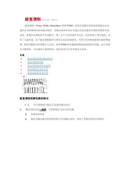
目录
∙脉宽调制变频电路的特点
∙脉宽调制的原理
∙脉宽调制的典型电路图
∙脉宽调制技术的分类
∙脉宽调制的典型应用
脉宽调制变频电路的特点
∙ 1. 可以得到相当接近正弦波的输出电压
2. 整流电路采用二极管,可获得接近1的功率因数
3. 电路结构简单
4. 通过对输出脉冲宽度的控制可改变输出电压,加快了变频过程的动态响应。
外文原文Pulse-width modulationPulse-width modulation (PWM)is a modulation technique that conforms the width of the pulse, formally the pulse duration, based on modulator signal information. Although this modulation technique can be used to encode information for transmission, its main use is to allow the control of the power supplied to electrical devices, especially to inertial loads such as motors. In addition, PWM is one of the two principal algorithms used in photovoltaic solar battery chargers,[1]The average value of voltage (and current) fed to the load is controlled by turning the switch between supply and load on and off at a fast pace. The longer the switch is on compared to the off periods, the higher the power supplied to the load is.The PWM switching frequency has to be much faster than what would affect the load, which is to say the device that uses the power. Typically switchings have to be done several times a minute in an electric stove, 120 Hz in a lamp dimmer, from few kilohertz (kHz) to tens of kHz for a motor drive and well into the tens or hundreds of kHz in audio amplifiers and computer power supplies.The term duty cycle describes the proportion of 'on' time to the regular interval or 'period' of time; a low duty cycle corresponds to low power, because the power is off for most of the time. Duty cycle is expressed in percent, 100% being fully on.The main advantage of PWM is that power loss in the switching devices is very low. When a switch is off there is practically no current, and when it is on, there is almost no voltage drop across the switch. Power loss, being the product of voltage and current, is thus in both cases close to zero. PWM also works well with digital controls, which, because of their on/off nature, can easily set the needed duty cycle.PWM has also been used in certain communication systems where its duty cycle has been used to convey information over a communications channel.HistoryIn the past, when only partial power was needed (such as for a sewing machine motor), a rheostat (located in the sewing machine's foot pedal) connected in series with the motor adjusted the amount of current flowing through the motor, but also wasted power as heat in the resistor element. It was an inefficient scheme, but tolerable because the total power was low. This was one of several methods of controlling power. There were others—some still in use—such as variable autotransformers, including thetrademarked 'Autrastat' for theatrical lighting; and the Variac, for general AC power adjustment. These were quite efficient, but also relatively costly.For about a century, some variable-speed electric motors have had decent efficiency, but they were somewhat more complex than constant-speed motors, and sometimes required bulky external electrical apparatus, such as a bank of variable power resistors or rotating converter such as Ward Leonard drive.However, in addition to motor drives for fans, pumps and robotic servos, there was a great need for compact and low cost means for applying adjustable power for many devices, such as electric stoves and lamp dimmers.One early application of PWM was in the Sinclair X10, a 10 W audio amplifier available in kit form in the 1960s. At around the same time PWM started to be used in AC motor control.Fig. 1: a pulse wave, showing the definitions of , and D.Pulse-width modulation uses a rectangular pulse wave whose pulse width is modulated resulting in thevariation of the average value of the waveform. If we consider a pulse waveform , with period ,low value , a high value and a duty cycle D (see figure 1), the average value of thewaveform is given by:As is a pulse wave, its value is for and for. The above expression then becomes:This latter expression can be fairly simplified in many cases where as. From this, it is obvious that the average value of the signal () is directly dependent on the duty cycle D大连交通大学2014届本科生毕业论文外文翻译Fig. 2: A simple method to generate the PWM pulse train corresponding to a given signal is the intersective PWM: the signal (here the red sinewave) is compared with a sawtooth waveform (blue). When the latter is less than the former, the PWM signal (magenta) is in high state (1). Otherwise it is in the low state (0).The simplest way to generate a PWM signal is the intersective method, which requires only a sawtooth or atriangle waveform (easily generated using a simple oscillator) and a comparator. When the value of the reference signal (the red sine wave in figure 2) is more than the modulation waveform (blue), the PWM signal (magenta) is in the high state, otherwise it is in the low state.Time proportioningMany digital circuits can generate PWM signals (e.g., many microcontrollers have PWM outputs). They normally use a counter that increments periodically (it is connected directly or indirectly to the clock of the circuit) and is reset at the end of every period of the PWM. When the counter value is more than the reference value, the PWM output changes state from high to low (or low to high).[3]This technique is referred to as time proportioning, particularly as time-proportioning control[4]– which proportion of a fixed cycle time is spent in the high state.The incremented and periodically reset counter is the discrete version of the intersecting method's sawtooth. The analog comparator of the intersecting method becomes a simple integer comparison between the current counter value and the digital (possibly digitized) reference value. The duty cycle can only be varied in discrete steps, as a function of the counter resolution. However, a high-resolution counter can provide quite satisfactory performance.PWM sampling theoremThe process of PWM conversion is non-linear and it is generally supposed that low pass filter signal recovery is imperfect for PWM. The PWM sampling theorem[6] shows that PWM conversion can be perfect. The theorem states that "Any bandlimited baseband signal within ±0.637 can be represented by a pulsewidth modulation (PWM) waveform with unit amplitude. The number of pulses in the waveform is equal to the number of Nyquist samples and the peak constraint is independent of whether the waveform is two-level or three-level."Power deliveryPWM can be used to control the amount of power delivered to a load without incurring the losses that would result from linear power delivery by resistive means. Potential drawbacks to this technique are the pulsations defined by the duty cycle, switching frequency and properties of the load. With a sufficiently high switching frequency and, when necessary, using additional passive electronic filters, the pulse train can be smoothed and average analog waveform recovered.High frequency PWM power control systems are easily realisable with semiconductor switches. As explained above, almost no power is dissipated by the switch in either on or off state. However, during the transitions between on and off states, both voltage and current are nonzero and thus power is dissipated in the switches. By quickly changing the state between fully on and fully off (typically less than 100 nanoseconds), the power dissipation in the switches can be quite low compared to the power being delivered to the load.Modern semiconductor switches such as MOSFETs or Insulated-gate bipolar transistors (IGBTs) are well suited components for high efficiency controllers. Frequency converters used to control AC motors may have efficiencies exceeding 98%. Switching power supplies have lower efficiency due to low output voltage levels (often even less than 2 V for microprocessors are needed) but still more than 70–80% efficiency can be achieved.Variable-speed fan controllers for computers usually use PWM, as it is far more efficient when compared to a potentiometer or rheostat. (Neither of the latter is practical to operate electronically; they would require a small drive motor.)Light dimmers for home use employ a specific type of PWM control. Home-use light dimmers typically include electronic circuitry which suppresses current flow during defined portions of each cycle of the AC line voltage. Adjusting the brightness of light emitted by a light source is then merely a matter of setting at what voltage (or phase) in the AC halfcycle the dimmer begins to provide electrical current to the light source (e.g. by using an electronic switch such as a triac). In this case the PWM duty cycle is the ratio of the conduction time to the duration of the half AC cycle defined by the frequency of the AC line voltage (50 Hz or 60 Hz depending on the country).V oltage regulationMain article: Switched-mode power supplyPWM is also used in efficient voltage regulators. By switching voltage to the load with the appropriate duty cycle, the output will approximate a voltage at the desired level. The switching noise is usually filtered with an inductor and a capacitor.One method measures the output voltage. When it is lower than the desired voltage, it turns on the switch. When the output voltage is above the desired voltage, it turns off the switch.Audio effects and amplificationPWM is sometimes used in sound (music) synthesis, in particular subtractive synthesis, as it gives a sound effect similar to chorus or slightly detuned oscillators played together. (In fact, PWM is equivalent to the difference of two sawtooth waves with one of them inverted.[1]) The ratio between the high and low level is typically modulated with a low frequency oscillator. In addition, varying the duty cycle of a pulse waveform in a subtractive-synthesis instrument creates useful timbral variations. Some synthesizers have a duty-cycle trimmer for their square-wave outputs, and that trimmer can be set by ear; the 50% point (true square wave) was distinctive, because even-numbered harmonics essentially disappear at 50%. Pulse waves, usually 50%, 25%, and 12.5%, make up the soundtracks of classic video games.A new class of audio amplifiers based on the PWM principle is becoming popular. Called "Class-D amplifiers", they produce a PWM equivalent of the analog input signal which is fed to the loudspeaker via大连交通大学2014届本科生毕业论文外文翻译a suitable filter network to block the carrier and recover the original audio. These amplifiers are characterized by very good efficiency figures (≥ 90%) and compact size/light weight for large power outputs. For a few decades, industrial and military PWM amplifiers have been in common use, often for drivingservo motors. Field-gradient coils in MRI machines are driven by relatively high-power PWM amplifiers.Historically, a crude form of PWM has been used to play back PCM digital sound on the PC speaker, which is driven by only two voltage levels, typically 0 V and 5 V. By carefully timing the duration of the pulses, and by relying on the speaker's physical filtering properties (limited frequency response, self-inductance, etc.) it was possible to obtain an approximate playback of mono PCM samples, although at a very low quality, and with greatly varying results between implementations.In more recent times, the Direct Stream Digital sound encoding method was introduced, which uses a generalized form of pulse-width modulation called pulse density modulation, at a high enough sampling rate (typically in the order of MHz) to cover the whole acoustic frequencies range with sufficient fidelity. This method is used in the SACD format, and reproduction of the encoded audio signal is essentially similar to the method used in class-D amplifiers.中文翻译一、脉冲宽度调制脉冲宽度调制(PWM),是一种在一定的脉冲持续时间内,基于调制信号来追踪所希望达到的脉冲宽度的调制方式。
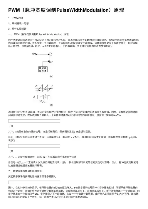
PWM(脉冲宽度调制PulseWidthModulation)原理1、 PWM原理2、调制器设计思想3、具体实现设计⼀、 PWM(脉冲宽度调制Pulse Width Modulation)原理:脉冲宽度调制波通常由⼀列占空⽐不同的矩形脉冲构成,其占空⽐与信号的瞬时采样值成⽐例。
图1所⽰为脉冲宽度调制系统的原理框图和波形图。
该系统有⼀个⽐较器和⼀个周期为Ts的锯齿波发⽣器组成。
语⾳信号如果⼤于锯齿波信号,⽐较器输出正常数A,否则输出0。
因此,从图1中可以看出,⽐较器输出⼀列下降沿调制的脉冲宽度调制波。
通过图1b的分析可以看出,⽣成的矩形脉冲的宽度取决于脉冲下降沿时刻t k时的语⾳信号幅度值。
因⽽,采样值之间的时间间隔是⾮均匀的。
在系统的输⼊端插⼊⼀个采样保持电路可以得到均匀的采样信号,但是对于实际中tk-kTs<(1)其中,x{t}是离散化的语⾳信号;Ts是采样周期;是未调制宽度;m是调制指数。
然⽽,如果对矩形脉冲作如下近似:脉冲幅度为A,中⼼在t = k Ts处,在相邻脉冲间变化缓慢,则脉冲宽度调制波x p(t)可以表⽰为:(2)其中,。
⽆需作频谱分析,由式(2)可以看出脉冲宽度信号由语⾳信号x(t)加上⼀个直流成分以及相位调制波构成。
当时,相位调制部分引起的信号交迭可以忽略,因此,脉冲宽度调制波可以直接通过低通滤波器进⾏解调。
⼆、数字脉冲宽度调制器的实现:实现数字脉冲宽度调制器的基本思想参看图2。
图中,在时钟脉冲的作⽤下,循环计数器的5位输出逐次增⼤。
5位数字调制信号⽤⼀个寄存器来控制,不断于循环计数器的输出进⾏⽐较,当调制信号⼤于循环计数器的输出时,⽐较器输出⾼电平,否则输出低电平。
循环计数器循环⼀个周期后,向寄存器发出⼀个使能信号EN,寄存器送⼊下⼀组数据。
在每⼀个计数器计数周期,由于输⼊的调制信号的⼤⼩不同,⽐较器输出端输出的⾼电平个数不⼀样,因⽽产⽣出占空⽐不同的脉冲宽度调制波。

脉冲宽度调制————————————————————————————————作者:————————————————————————————————日期:ﻩ脉冲宽度调制脉冲宽度调制(PWM),是英文“Pulse Width Modulation”的缩写,简称脉宽调制,是利用微处理器的数字输出来对模拟电路进行控制的一种非常有效的技术,广泛应用在从测量、通信到功率控制与变换的许多领域中。
目录1简介2背景介绍3基本原理4谐波频谱5具体过程6优点7控制方法8应用领域9具体应用1简介脉冲宽度调制是一种模拟控制方式,其根据相应载荷的变化来调制晶体管基极或MOS管栅极的偏置,来实现晶体管或MOS管导通时间的改变,从而实现开关稳压电源输出的改变。
这种方式能使电源的输出电压在工作条件变化时保持恒定,是利用微处理器的数字信号对模拟电路进行控制的一种非常有效的技术。
PWM控制技术以其控制简单,灵活和动态响应好的优点而成为电力电子技术最广泛应用的控制方式,也是人们研究的热点。
由于当今科学技术的发展已经没有了学科之间的界限,结合现代控制理论思想或实现无谐振软开关技术将会成为PWM控制技术发展的主要方向之一。
2背景介绍随着电子技术的发展,出现了多种PWM技术,其中包括:相电压控制PWM、脉宽PWM法、随机PWM、SPWM法、线电压控制PWM等,而在镍氢电池智能充电器中采用的脉宽PWM法,它是把每一脉冲宽度均相等的脉冲列作为PWM波形,通过改变脉冲列的周期可以调频,改变脉冲的宽度或占空比可以调压,采用适当控制方法即可使电压与频率协调变化。
可以通过调整PWM的周期、PWM的占空比而达到控制充电电流的目的。
模拟信号的值可以连续变化,其时间和幅度的分辨率都没有限制。
9V电池就是一种模拟器件,因为它的输出电压并不精确地等于9V,而是随时间发生变化,并可取任何实数值。
与此类似,从电池吸收的电流也不限定在一组可能的取值范围之内。
模拟信号与数字信号的区别在于后者的取值通常只能属于预先确定的可能取值集合之内,例如在{0V,5V}这一集合中取值。
脉冲宽度调制电路的设计与实现英文Pulse Width Modulation Circuit Design and Implementation IntroductionPulse Width Modulation (PWM) is a commonly used technique in power electronics to control the amount of power delivered to a load. It involves varying the width of a pulse with respect to a period, where the average voltage delivered to the load is proportional to the duty cycle of the pulse. In this article, we will discuss the design and implementation of a PWM circuit.Circuit DiagramThe PWM circuit consists of a Comparator, Astable Multivibrator, RC circuit and a Power MOSFET. The circuit diagram is shown below:[Insert Circuit Diagram]Working PrincipleThe operation of the PWM circuit can be understood by the following steps:1. A triangle wave signal is generated by the Astable Multivibrator with a frequency f.2. The output of the Astable Multivibrator is compared with a DC voltage signal Vref by the Comparator.3. The Comparator output switches between high and low depending on the comparison result.4. The RC circuit filters the Comparator output signal to obtain a PWM signal.5. The Power MOSFET switches on and off according to the PWM signal, delivering power to the load.Design ConsiderationsThe following design considerations should be taken into account while designing the PWM circuit:1. The frequency of the Astable Multivibrator should be chosen to be higher than the maximum frequency of the load.2. The amplitude of the triangle wave should be large enough to allow sufficient variation of the duty cycle.3. The value of the RC circuit should be chosen such that the filtered PWM signal has a smooth transition between high and low states.4. The Power MOSFET should be chosen such that it can operate at the frequency of the PWM signal and handle the power delivered to the load.ImplementationThe following steps should be followed while implementing the PWM circuit:1. Choose appropriate values for the components according to the design considerations.2. Construct the circuit on a breadboard, using a Power MOSFET of appropriate rating.3. Connect a load to the output of the Power MOSFET andverify its operation using an oscilloscope.4. Test the circuit at different duty cycles and measure the voltage and current delivered to the load.5. Modify the circuit or choose different components if necessary to achieve the desired performance.ConclusionIn this article, we discussed the design and implementation of a PWM circuit. PWM is a widely used technique in power electronics to control the output power of a load. By following the design considerations and implementation steps,engineers can design and build PWM circuits for various applications.。
直流脉宽调制(PWM)变换器
直流pwn变换器在一个开关周期内;当0
什么是PWM脉宽调制脉冲宽度调制(PWM),是英文“Pulse Width Modulation”的缩写,简称脉宽调制,是利用微处理器的数字输出来对模拟电路进行控制的一种非常有效的技术,广泛应用在从测量、通信到功率控制与变换的许多领域中
所谓脉宽,其实就是指脉冲的宽度。
举个例:我们放一盆水,一直不停的放要1分钟放满,但我为了控制放满的时间,在每一秒的时间里需要开一下,关一下。
而这开和关的时间比值就可以认为是脉冲的占空比,开的时间长,相应的关的时间就会缩短(每秒必须完成一次开和关,相当于脉冲的频率)。
而放满的时间就可以通过这样的方式来调节(相当于控制输出)这样通过调整开和关的时间(脉冲宽度)来调整输出的,就是脉宽调制。
基本原理控制方式就是对逆变电路开关器件的通断进行控制,使输出端得到一系列幅值相等的脉冲,用这些脉冲来代替正弦波或所需要的波形。
也就是在输出波形的半个周期中产生多个脉冲,使各脉冲的等值电压为正弦波形,所获得的输出平滑且低次谐波少。
优点:从处理器到被控系统信号都是数字形式的,无需进行数模转换。
让信号保持为数字形式可将噪声影响降到最小。
噪声只有在强到足以将逻辑1改变为逻辑0或将逻辑0改变为逻辑1时,也才能对数字信号产生影响。
相关链接什么是直流pwm变换器直流PWM 变换器的原理。
直流电机脉冲宽度调制(Pulse Width Modwtated-简称PWM)调速系统产生于70年代中期.最早用于不可逆、小功率驱动,例如自动跟踪天文望远镜、自动记录仪表等。
近十多年来,由于晶体管器件水平的提高及电路技术的发展,同时又因出现了宽调速永磁直流电机, 它们之间的结合促使PWM技术的高速发展,并使电气驱动技术推进到一个新的高度.在国外,PWM最早是在军事工业以及空间技术中应用。
它以优越的性能,满足那些高速度、高精度随动跟踪系统的需求。
近八、九年来,进一步扩散到民用工业,特别是在机床行业、自动生产线及机器人等领域中广泛应用。
可以这样说,六十年代中期发展起来的晶体管OTL电路、OCL电路,特别是桥型无变压器输出的BTL电路,为PWM系统的发展奠定了电路基础,而各种先进的功率器件(如GTR,IGBT模块等)及宽调速直流电机的出现,更为PWM技术的应用提供了良好的条件。
PWM系统的特点1)开关损耗小,变流器效率高。
2)系统主回路电源是经过整流及大容量电容器虑波后供电,因而不会因电网电压波形的失真而影响调节质量。
3)以1KHZ-8KHZ的高频脉冲电流给电机的电枢供电,由于是感性负载,脉冲电流得以滤平,所以波系数小,电机发热量小,可以减小机械变形,从而能提高工作机械的精度。
也正是由于波形系数小,电机利用率高,从相同发热量的角度考虑,PWM 系统获得可以比SCR系统高1.3-1.8倍的转矩,因此PWM系统可以选用较小容量的电机.特别是工作在正反转频繁的伺服系统中,其优点尤为突出。
4)系统的响应频带很宽,可达到100-200HZ以上。
因此起制动非常快,而且超调量小,可以大大提高高冲击率机械的生产效率。
5)因系统采样频率高,频带宽,所以抗负载扰动的性能好,动态速度下降小,恢复时间快,因此动态硬度好,加工零件表面光洁度高。
6)同样由于采样频率高,避开了电机及传动机械的共振点,所以运动平稳,这也是提高加工光洁度的一个有利因素。
24.437 Power ElectronicsSinusoidal Pulse width modulationThe switches in the voltage source inverter(See Fig.1)can be turned on and off as required.In the simplest approach,the top switch is turned on If turned on and off only once in each cycle,a square wave waveform results.However,if turned on several times in a cycle an improved har- monic profile may be achieved.Fig 1:Simple Voltage SourcedIn the most straightforward implementation,generation of the desired output voltage is achieved by comparing the desired reference waveform(modulating signal)with a high-frequency triangu- lar‘carrier’wave as depicted schematically in Fig.2.Depending on whether the signal voltage is larger or smaller than the carrier waveform,either the positive or negative dc bus voltage is applied at the output.Note that over the period of one triangle wave,the average voltage appliedto the load is proportional to the amplitude of the signal(assumed constant)during this period.The resulting chopped square waveform contains a replica of the desired waveform in its low fre- quency components,with the higher frequency components being at frequencies of an close to the carrier frequency.Notice that the root mean square value of the ac voltage waveform is still equal to the dc bus voltage,and hence the total harmonic distortion is not affected by the PWM process. The harmonic components are merely shifted into the higher frequency range and are automati- cally filtered due to inductances in the ac system.When the modulating signal is a sinusoid of amplitude Am,and the amplitude of the triangular carrier is Ac,the ratio m=Am/Ac is known as the modulation index.Note that controlling the modulation index therefor controls the amplitude of the applied output voltage.With a sufficiently high carrier frequency(see Fig.3 drawn for fc/fm=21 and t=L/R=T/3;T=period of funda- mental),the high frequency components do not propagate significantly in the ac network(or load) due the presence of the inductive elements.However,a higher carrier frequency does result in a larger number of switchings per cycle and hence in an increased power loss.Typically switching frequencies in the 2-15 kHz range are considered adequate for power systems applications.Alsoin three-phase systems it is advisable to use s so that all three waveforms are symmetric.Fig 2:Principal of Pulse Width ModulationFig.3:SPWM with fc/fm=48,L/R=T/3Note that the process works well for m ≤1.For m >1,there are periods of the triangle wave in which there is no intersection of the carrier and the signal as in Fig.4.However,a certain amountof this“overmodulation”is often allowed in the interest of obtaining a larger ac voltage magni- tude even though the spectral content of the voltage is rendered somewhat poorer.Note that with an odd ratio for fc/fm,the waveform is anti-symmetric over a 360 degree cycle. With an even number,there are harmonics of even order,but in particular also a small dc compo- nent.Hence an even number is not recommended for single phase inverters,particularly for smal ratios of fc/fm.SPWM Spectra:Although the SPWM waveform has harmonics of several orders in the phase voltage waveform, the dominant ones other than the fundamental are of order n and n±2 where n=fc/fm.This is evi- dent for the spectrum for n=15 and m=0.8 shown in Fig.5.Note that if the other two phases are identically generated but 120o apart in phase,the line-line voltage will not have any triplenhar-monics.Hence it is advisable to choose,as then the dominant harmonic will be eliminated.It is evident from Fig 5b,that the dominant 15th harmonic in Fig.5a is effectively eliminated in the line voltage.Choosing a multiple of 3 is also convenient as then the same trian- gular waveform can be used as the carrier in all three phases,leading to some simplification in hardware.It is readily seen that as the where E is the dc bus voltage,that the rms valueof the output voltage signal is unaffected by the PWM process.This is strictly true for the phase voltage as triplen harmonic orders are cancelled in the line voltage.However,the problematic har- monics are shifted to higher orders,thereby making filtering much easier.Often,the filtering is carried out via the natural high-impedance characteristic of the load.Fig.5:SPWM Harmonic Spectra:n=15,m=0.Selective Harmonic Elimination(also called Optimal PWM)Notice that in the SPWM strategy developed above,a large number of switchings are required, with the consequent associated switching losses.With the method of Selective Harmonic Elimina- tion,only selected harmonics are eliminated with the smallest number of switchings.This method however can be difficult to implement on-line due to computation and memory requirements. For a two level PWM waveform with odd and halfwave symmetries and n chops per quarter cycleas shown in Fig 4,the peak magnitude of the harmonic components including the fundamental,are given byEqn.1:Here is the magnitude of the harmonic and is the primary switching angle.Even har- monics do not show up because of the half-wave symmetry.The n chops in the waveform afford n degrees of freedom.Several control options are thus possi- ble.For example n selected harmonics can be eliminated.Another option which is used here is to eliminate n-1 selected harmonics and use the remaining degree of freedom to control the funda- mental frequency ac voltage.To find theα’s required to achieve this objective,it is sufficient to set the corresponding h’s in the above equations to the desired values(0 for the n-1 harmonics to be eliminated and the desired per-unit ac magnitude for the fundamental)and solve for theα’s.Fig 4:A two-level PWM waveform with odd and halfwave symmEquation 1 can be readily proved by finding the fourier coefficients of the waveform shown inFig.4.In general,for a periodic waveform with period,the Fourier Cosine and Sine Coeffi- cients are given by:Because of the half-cycle symmetry of the waveform of Fig.4,only odd order harmonics exist. Also,it is easy to see that the Fourier Cosine coefficients disappear with the choice of coordinateaxes used.Utilizing the quarter cycle symmetry,the Fourier Sine coefficients become:Substituting the two-valued pwm waveform for,one obtains(see Fig.4):The following example illustrates the use of three chops per quarter cycle which allow for three degrees of freedom.We may use these to eliminate two harmonics and control the magnitude of the fundamental to any desired value:Example:Selective Harmonic Elimination is applied with a view to controlling the fundamental component of voltage to 50V(rms)and eliminating the 3rd and 5th harmonics.The source voltage is 100 V. Calculate the required chopping angles.As three objectives are to be achieved,we need 3 chops.The fundamental,3rd and 5th harmonic magnitudes are given by:We require:翻译24.437电力电子正弦脉宽调制电压源逆变器的开关(见图1)可以按要求打开和关闭。
中英文资料外文翻译文献(文档含英文原文和中文翻译)ARM Cortex-M3脉宽调制器(PWM)与通用定时器1.PWM脉宽调制(PWM)是一项功能强大的技术,它是一种对模拟信号电平进行数字化编码的方法。
在脉宽调制中使用高分辨率计数器来产生方波,并且可以通过调整方波的占空比来对模拟信号电平进行编码。
PWM通常使用在开关电源(switching power)和电机控制中。
StellarisPWM模块由3个PWM发生器模块1个控制模块组成。
每个PWM 发生器模块包含1个定时器(16位递减或先递增后递减计数器),2个PWM比较器,PWM信号发生器,死区发生器和中断/ADC-触发选择器。
而控制模块决定了PWM 信号的极性,以及将哪个信号传递到管脚。
每个PWM发生器模块产生两个PWM信号,这两个PWM信号可以是独立的信号(基于同一定时器因而频率相同的独立信号除外),也可以是一对插入了死区延迟的互补(complementary)信号。
这些PWM发生模块的输出信号在传递到器件管脚之前由输出控制模块管理。
StellarisPWM模块具有极大的灵活性。
它可以产生简单的PWM信号,如简易充电泵需要的信号;也可以产生带死区延迟的成对PWM信号,如供半-H桥(half-H bridge)驱动电路使用的信号。
3个发生器模块也可产生3相反相器桥所需的完整6通道门控。
PWM定时器每个PWM发生器的定时器都有两种工作模式:递减计数模式或先递增后递减计数模式。
在递减计数模式中,定时器从装载值开始计数,计数到零时又返回到装载值并继续递减计数。
在先递增后递减计数模式中,定时器从0开始往上计数,一直计数到装载值,然后从装载值递减到零,接着再递增到装载值,依此类推。
通常,递减计数模式是用来产生左对齐或右对齐的PWM信号,而先递增后递减计数模式是用来产生中心对齐的PWM信号。
PWM定时器输出3个信号,这些信号在生成PWM信号的过程中使用:方向信号(在递减计数模式中,该信号始终为低电平,在先递增后递减计数模式中,则是在低高电平之间切换);当计数器计数值为0时,一个宽度等于时钟周期的高电平脉冲;当计数器计数值等于装载值时,一个宽度等于时钟周期的高电平脉冲。
dram读取脉冲宽度-回复什么是脉冲宽度调制脉冲宽度调制(Pulse Width Modulation,PWM)是一种用于控制电子设备的方法,通过改变信号脉冲的宽度来控制输出电压或功率。
这种技术可以被广泛应用于不同的领域,包括电力电子、通信和自动化等。
脉冲宽度调制技术可以提供精确的控制,并且在相对较低的成本下实现。
脉冲宽度调制的原理脉冲宽度调制的原理基于一个重要的概念,即脉冲宽度和平均功率或电压之间存在一种线性关系。
换句话说,当脉冲的宽度增加时,平均功率或电压也会随之增加。
例如,考虑一个脉冲信号,其由高电平和低电平构成。
通过改变高电平的持续时间(即脉冲宽度),可以实现不同的平均功率或电压输出。
如果高电平的持续时间比低电平的持续时间长,那么平均功率或电压将更高。
相反,如果高电平的持续时间比低电平的持续时间短,那么平均功率或电压将更低。
如何实现脉冲宽度调制实现脉冲宽度调制的方法有很多种。
下面介绍两种常见的方法:1. 定时器/计数器:这是一种基于硬件的方法,通过使用定时器和计数器来生成脉冲宽度调制信号。
使用这种方法,可以设置定时器的时钟频率和计数器的计数阈值,以控制脉冲的宽度和周期。
通过调整计数阈值,可以改变脉冲的宽度,从而实现对输出的控制。
2. 微控制器:这是一种基于软件的方法,通过编程微控制器来生成脉冲宽度调制信号。
微控制器具有内置的定时器和计数器,使得编程变得更加简单。
程序可以定期地修改计数器的计数值,从而改变脉冲的宽度。
通过编程微控制器,可以实现非常精确和灵活的脉冲宽度调制控制。
脉冲宽度调制在实际应用中的应用脉冲宽度调制在许多实际应用中都发挥了重要的作用。
以下是一些常见的应用领域:1. 电力电子:脉冲宽度调制被广泛应用于交流电变直流电的电力电子设备中,如逆变器和整流器。
通过控制脉冲的宽度,可以实现对输出电压和电流的精确调节。
2. 数字通信:脉冲宽度调制被广泛应用于数字通信领域中,如有线和无线通信系统。
(名词解释)脉宽调制
脉冲宽度调制(PWM),是英文“Pulse Width Modulation”的缩写,简称脉宽调制,是利用微处理器的数字输出来对模拟电路进行控制的一种非常有效的技术,广泛应用在从测量、通信到功率控制与变换的许多领域中。
PWM是一种对模拟信号电平进行数字编码的方法。
通过高分辨率计数器的使用,方波的占空比被调制用来对一个具体模拟信号的电平进行编码。
PWM信号仍然是数字的,因为在给定的任何时刻,满幅值的直流供电要么完全有(ON),要么完全无(OFF)。
电压或电流源是以一种通(ON)或断(OFF)的重复脉冲序列被加到模拟负载上去的。
通的时候即是直流供电被加到负载上的时候,断的时候即是供电被断开的时候。
只要带宽足够,任何模拟值都可以使用PWM进行编码。
附录A 译文脉宽调制技术前面讨论的三相6阶梯逆变器既有其优点也有其局限性。
由于在基波频率的每个周期仅开关六次,因此逆变器的控制简单而且开关损耗低。
但是6阶梯波电压中的低次谐波会导致电流波形产生极大的畸变,除非使用笨重庞大的不经济的低通滤波器滤波。
另外,输出电压靠整流器控制,也不可避免的带有整流器所具有的通常的缺点[16]。
脉宽调制(PWM )工作原理由于逆变器中电子开关的存在,在恒定的直流输入电压d V 作用下,逆变器可以通过自身的多次开关控制输出电压并优化输出谐波。
图5-18解释了通过PWM 控制输出电压的工作原理。
基波电压1v 在方波工作模式下具有最大的幅值(4d v / )。
如图示,通过产生俩个凹口,1v 的幅值可以被减小,随着凹口宽度的增加,基波电压将随之减小。
图5-18 PWM 控制输出电压的工作原理PWM 分类在过去的文献中已提出了很多的PWM 技术,下面是对这些PWM 技术的分类。
1)正弦PWM (SPWM );2)特定谐波消除PWM (SHEPWM );3)最小纹波电流PWM ;4)空间矢量PWM (SVW );5)随机PWM ;6)滞环电流控制PWM ;7) 瞬时电流控制正弦PWM ;8)Delta 调制PWM ;9)Sigma Delta 调制PWM通常PWM 技术可以按电压控制或电流控制来分类,或按前馈方式或反馈方式来分类,也可以按基于斩波或不基于斩波来分类。
注意,前面讨论的移相控制PWM 也是一种PWM 技术。
在这一节中,将对主要的PWM 技术做一简单的回顾。
5.5.1正弦PWM正弦PWM 技术在实际的工业变流器的应用中非常普及。
这项技术在文献中已经得到了广泛的讨论。
图5-19解释了SPWM 的基本工作原理。
图中频率为c f 的等腰三角载波与频率f 的正弦调制波相比较,两者的焦点确定了电力电子器件的开关时刻。
例如,图中给出了开关半桥逆变器中的14Q Q 构成的a0v 波形,为防止14Q Q 的同时导通而设计的14Q Q 之间的死区时间在图中被忽略了。
上述方法也被称为三角波法,次谐波法或次震荡法。
a0v 波形的脉冲及凹口宽度按正弦规律变化,从而使其基波成分的频率等于f 且幅值正比于指令调制电压。
如图5-20给出了负载无中线连接的典型的线电压的相电压波形。
a0v 波形的傅立叶分析可以由下式给出:)高频成分()(w w wt sin m 5.0v c d 0a N M V ±++=ϕ (5-33)图5-19 三相桥式逆变器正弦PWM 的工作原理式中,m 为调制指数;w 为基波频率(rad/s ),(与调制频率相同);ϕ为输出相位移,取决于调制波的实际位置。
图5-20 PWM 逆变器的线电压和相电压的波形a )线电压b )相电压调制指数m 被定义T P m V V =(5-34)式中,P V 为调制波的峰值;T V 为载波的峰值。
理想情况下,m 可以从0变化到1,并且调制波与输出波形之间将保持着线性关系。
逆变器基本上可以被看作是一个线性放大器,根据(5-33)和式(5-34)可以得出这个放大器的增益G 为:T V V V V G d P d 5.0m 5.0== (5-35) 当m=1时,可以得到最大的基波电压峰值0.5d V ,这个数值是方波电压输出时基波电压峰值(4d v /2π)的78.55%。
事实上,通过将某些三次谐波成分加入到调制波中,线性工作范围的最大输出基波电压峰值可以增加到方波输出时的90.7%。
当m=0时,a0v 是一个频率与载波频率相同,脉冲和凹口宽度上下对称的方波。
PWM 输出波形中,含有与载波频率相关且边(频)带与调制波频率相关的谐波成分。
这些频率成分可以表示为w w c N M ±,如式(5-33)所示。
式中,M 和N 均为整数;M+N 为一个奇整数。
表5-1给出了当载波频率与调制波频率的比值c w /w 15P ==时的输出谐波。
表5-1 SPWM 在15w /w c =时的输出谐波由上述的输出谐波成分可以推导出,其幅值与载波比P 无关,并将随着M 和N 的增大而减小。
随着载波比的P 的增大,逆变器输出线电流谐波将通过电机的漏电感得到更好的滤波,并接近于正弦波。
选择载波频率需要折中考虑逆变器损耗和点击损耗。
高的载波频率(与开关频率相同)将使逆变的开关损耗增加,但会减少电机的谐波损耗。
最有的载波频率选择应使系统的总损耗减小。
PWM 开关频率的一个重要影响是当逆变器向电机提供功率时由磁滞效应产生的噪声(也称为磁噪声)。
这种噪声可以通过随机的改变PWM 开关频率而减轻(随机SPWM ),通过吧开关频率增加到高于音频范围,也可以把这种噪声完全消除。
现代高速IGBT 可以很容易的实现这种无音频噪声的变频传动。
逆变器输出端的低通滤波器也可以消除这种噪声。
1.过调制区操作 当调制指数m 接近于1时,在正,负半周期中间位置附近的凹口和脉冲将趋于消失。
为了使器件能有一个完整的开关操作,应保持一个最小的凹口和脉冲宽度。
当这个最小脉宽的凹口和脉冲消失时,负载电流会有一个瞬态跳变。
对IGBT 逆变器,这个跳变可能是比较小的;但对于电力GTO晶闸管逆变器,由于器件变速的开关,这个跳变会很大。
m的数值可以增加到大于1进入准PWM区域,图5-21所示为正半周期操作。
图中a0v在正半周期中间附近脉冲向下的凹口不见了,从而给出了一个具有较高的基波成分的准方波输出。
如图5-22所示,在过调区,传递特性是非线性的,波形中重新出现了5次和7次谐波成分。
随着m数值的增加,即调制信号的增大,最终逆变器将给出一个方波输出,器件在方波的上升沿开关一次,在下降沿开关一次。
在这种情况下,输出基波相电压峰值达到4(0.5d V)/ ,即达到100%的输出,如图5-22所示。
图5-21 过调制区的波形图5-22 SPWM过调制输出传递特性2.载波与调制波频率的关系对于变速传动,逆变器输出电压和频率应按图2-14所示关系变化。
在恒功率区,逆变器以方波模式工作从而可以获得最大电压。
在恒转矩区,逆变器输出电压可以采用PWM控制。
通常希望逆变器工作时载波与调制波频率比P为一整数,即在整个工作范围内调制波与载波保持同步。
但当P保持为一定值,在基波频率下降时,会使载波频率也随之变得很低,就电机的谐波损耗而言,这通常是不希望的。
图5-23给出了一个GTO晶闸管逆变器实际的载波与基波频率的关系。
当基波频率很低时,载波频率保持恒定。
逆变器以自由运行方式或称一部模式工作。
在这个区域,载波比P可以是一个非整数,相位可能连续的移动,这将会产生谐波问题以及变化的直流偏移(差拍效应)。
随着f/fc数值的下降,这个问题会变得越发的严重。
在这里应该提及的是,与基波频率变化范围相比,现代IGBT器件的开关频率是非常高的,这使得PWM逆变器可以在整个异步范围内得到满意的操作。
如图5-23所示,在异步运行区后是同步区,在这个区,P以一种阶梯的方式变化,这使得最大和最小频率保持在设定边界值内的一个特定区域。
P 的数值总是保持为三的倍数,这是因为对无中线连接的负载,三的倍数次谐波是不需要考虑的。
当调制波频率接近于额定频率(f/f b =1)时,逆变器转换到方波模式工作,这里假设这是载波频率与基波频率相等。
在整个工作范围,控制策略应该仔细的设计,使在载波频率跳变的时刻,不产生电压的跳变,并且为了避免相邻P 值之间的抖动,在跳变点应设置一个窄的滞环带。
5-23 载波频率f/f b 的关系3.死区时间效应及补偿 由于死区(或封锁)效应,实际的PWM 逆变器的相电压(0a v )波形会在某种程度上偏离5-19所示的理想波形。
这种效应可以用图5-24中三相逆变桥中的a 相桥臂来解释。
电压源型逆变器的一个基本控制原则是要导通的器件应滞后于要关断的器件一个死区时间t d (典型值为几微妙)以防止峭壁的直通。
这是因为器件的导通是非常快的,而相对来说关断是比较慢的。
死区效应会导致输出电压的畸变并减小其幅值。
考虑图5-24所示PWM 操作,如图示,a 相电流i a 的方向为正。
初始状态Q 1为导通,0a v 的幅值为+0.5V d 。
Q 1在理想的开关点关断后,在Q 4导通前有一个时间间隔t d ,在这个间隔,Q 1和Q 4都处于关断状态,但+ i a 的流通使得0a v 在理想开关点自然的切换到-0.5 V d 。
现在考虑在理想开关点从Q 4到Q 1的带有延迟时间t d 的开关转换。
当Q 4Q 1两个器件都关断时,+i a 继续通过D 4流通,从而造成了如图所示阴影面积的脉冲伏-秒(V d t d )面积损失。
下面再考虑电流i a 的极性为负时的情况。
仔细的观察图示波形可以看到Q 4导通的前沿有一个类似的伏-秒面积的增加。
注意,上述伏-秒面积的损失或增加仅仅取决于电流的极性,而与电流的幅值无关。
图5-25给出了在每一个载波周期T c 分别对应于+i a 和-i a 的伏-秒面图5-24 半桥逆变器死区效应的波形 积(V d t d )损失和增加的积累效应对基波电压波形的影响。
图中基波电流i a 滞后于基波电压0a v 一个相位角ϕ。
图5-25中最下面的图解释了死区效应。
把由V d t d 构成的这些面积累加起来并在基波频率的半周期内加以平均可得出方波偏移电压V ε为d d c d d t f f 22t V V P V ==))((ε (5-36) 式中,P=f /f c ,f 为基波频率,图5-25中最上端的波形给出了V ε波对理想0a v 波的影响。
在较低的基波频率下,这种基波电压的损失以及低频谐波畸变会变得很严重。
死区效应可以很容易的通过电流反馈或电压反馈方法进行补偿。
对于点一种方法,通过对相电流极性的检测,将一个固定量的补偿偏移电压加到调制波上;对后一种方法,将检测的输出相电压与PWM 电压参数信号相对比,延后把偏差用于补偿PWM 参考调制波。
5.5.2 特定谐波消除PWM (SHEPWM )Tc=1/fcQ1Q1Q4td +0.5Vd+0.5Vd-0.5Vd-0.5VdVaoVao+ia -ia应用特定谐波消除PWM(SHEPWM)可以将方波中不希望有的低次谐波消除,并控制输出基波电压的大小,如图5-26所示。
在这种方法中,要在方波电压中开出一些预先确图5-25输出相电压波形的死区效应定好角度的凹槽。
图中所示为四分之一波对称的正半周波形,可以通过控制图中四个凹槽角1α,2α,3α和4α消除三个特定的谐波成分,同时控制输出基波电压。
如果图示波形中有更多的凹槽角,责可以消除更多的谐波成分。
图5-26 特定谐波消除PWM的相电压波形任何波形均可用如下傅立叶级数展开形似表示:v(t)=∑∞=+1 nnnsinwtb cosnwta)((5-37)式中⎰=ππ20n cosntdwt t v 1a )( (5-38) ⎰=ππ20n s i n n t d w t t v 1b )( (5-39)对于四分之一周期对称的波形,波形中将只含有正弦项,并且只含有几次谐波成分。