LTC3441 - 大电流微功率同步降压-升压型 DC-DC 转换器 LTC3441EDE
- 格式:pdf
- 大小:190.77 KB
- 文档页数:16
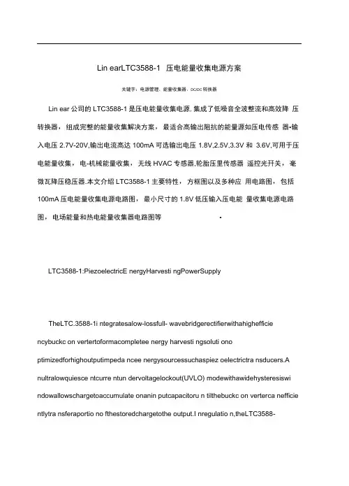
Lin earLTC3588-1 压电能量收集电源方案关键字:电源管理,能量收集器,DC/DC转换器Lin ear公司的LTC3588-1是压电能量收集电源,集成了低噪音全波整流和高效降压转换器,组成完整的能量收集解决方案,最适合高输出阻抗的能量源如压电传感器•输入电压2.7V-20V,输出电流高达100mA可选输出电压1.8V,2.5V,3.3V 和 3.6V,可用于压电能量收集,电-机械能量收集,无线HVAC专感器,轮胎压里传感器遥控光幵关,毫微瓦降压稳压器.本文介绍LTC3588-1主要特性,方框图以及多种应用电路图,包括100mA压电能量收集电源电路图,最小尺寸的1.8V低压输入压电能量收集电源电路图,电场能量和热电能量收集器电路图等•LTC3588-1:PiezoelectricE nergyHarvesti ngPowerSupplyTheLTC.3588-1i ntegratesalow-lossfull- wavebridgerectifierwithahighefficie ncybuckc on vertertoformacompletee nergy harvesti ngsoluti ono ptimizedforhighoutputimpeda ncee nergysourcessuchaspiez oelectrictra nsducers.A nultralowquiesce ntcurre ntun dervoltagelockout(UVLO) modewithawidehysteresiswi ndowallowschargetoaccumulate onanin putcapacitoru n tilthebuckc on verterca nefficie ntlytra nsferaportio no fthestoredchargetothe output.I nregulatio n,theLTC3588-1en tersasleepstate in whichboth in puta ndoutputquiesce ntcurre ntsare mini mal.T hebuckc on vertertur nsonan doffas neededtoma intain regulati on.Fouroutputvoltages,1.8V,2.5V,3.3Va nd3.6V,arepi nselectablewithupto100m Aofcontinu ousoutputcurre nt;however,theoutputcapacitormaybesizedtoservice ahigheroutputcurre ntburst.A nin putprotectivesh un tsetat20Ve nablesgreatere n ergystorageforagive namoun tofi nputcapacita nee.LTC3588-1主要特性:—NoLoad) 950nAln putQuiesce ntCurre nt(Outputi nRegulatio n450nAI nputQuiesce ntCurre nti nUVLO2.7Vto20VI nputOperati ngRa ngeIn tegratedLow-LossFull-WaveBridgeRectifierUptolOOmAofOutputCurre nt SelectableOutputVoltagesof1.8V,2.5V,3.3V,3.6VHighEfficie ncyl ntegratedHystereticBuckDC/DCIn putProtectiveShu nt —Upto25mAPull-Do wn atVIN> 20V WideI nputU ndervoltageLockout(UVLO)Ra ngeAvailablei n10-LeadMSEa nd3mmx3mmDFNPackagesLTC3588-1 应用:PiezoelectricE nergyHarvesti ngElectro-Mecha nicalE nergyHarvesti ngWirelessHVACSe nsors MobileAssetTracki ngTirePressureSe nsors BatteryReplaceme ntforl ndustrialSe nsors RemoteLightSwitchesStan dal on eNa nopowerBuckRegulator著一m函1.LTC3588匕8斎函」sm ApieicE一鱼S-rrl n E a yHaw邕?壬『OCT函 2.L T C3588—l 00m A te [>^K *t >[>M函i图3.LTC3588-13.3V 压电能量收集电源电路图:给带无线发送器的微处理器和 50mA 瞬态负载供电.P 旧电 SYSTEMS T220-.M*^3X_IDI —图4.最小尺寸的1.8V 低压输入压电能量收集电源电路图'h {OPTIONAL}VlH PGCXJDV||Q LTCK3B-1CAPsw D3 VoufDO1O|1FprePGOOOLTC3588-1$w^bur、蟻bl 1帕&0PIEZO STS T230-A4-M3XTtzu=1=T1-q —刖M|lF &vPflPZ? KWCW*|hUC358B-1.B . ¥IIE ■aiiiDI&3GND—■ JU -10UHI J-111FT2Li 卯—r- ?5V I -------1±图5.采用单个压电晶体和自动加电次序的双电源电路图iMU 比4优罚TWIflUHVOUTipF 6V—r^Ev1O0^亠*髦"F "T BYr1OyF25V I ----------------47|f图6.带备份电池的压电能量收集器电路图图7.AC 火线供电的3.6V 降压稳压器,大输出电容支持重负载PANELS ARE PLACED G bFROM T x4' FLUQRfSCFFJT LiflHT FIXTURESGOPPtR 用MEL(情綁刊IDANGER! HIGH VOLTAGE'COPPER PA 忡EL(12* x 24f \—F*GOODPGOQD9V ' BAntHVP1E2O SVSTEMS T2SOW-503XP21p 竝VlHPGOODITG33A8-1CAP SWV|W2Van00P22GHDPGOODPZ2PGOODlTCJ5B8-tswV,-,-vgyr□ lDO RND5p7?v-iPGOODLTO5^0-1GAP5W%V QUTBlI (X JHJ —*1O^F "T" SV图8.电场能量收集器电路图St _L5VT0 f6V•…SOUR PANfL rao5M4X&FrrIPF■VvVT BATTERYII%PiJOODLTG3W1GAP SWy IV3V CVT0001GNDiPG3OD5* 2.7V 蚀FX5V NESS SUPER W^ACITOR_ £5HSR-ODa30O^M2fl7图9.5-16V太阳能供电的2.5V电源,其超大电容增加输出能量存储和备份电池IPG-1 THERMALI GEMERATORMi 61-1,0-127-1.27I (TELLUflEX)—5,4VH工工工[---------1P22%卩GOODUC3506-1CAP畑V OUTDO01GUO跡47pF2.5V图10.热电能量收集器电路图。
同步降压-升压稳压器延长电池使用寿命
佚名
【期刊名称】《电子与电脑》
【年(卷),期】2005(000)001
【摘要】凌特公司(Linear Technology)推出真正降压-升压DC/DC转换器LTC3442。
该器件可在95%的效率提供高达1.2A的连续输出电流。
LTC3442是一个同步和固定频率的降压-升压DC/DC转换器,可用于由单节锂离子电池、多节碱性电池或镍氢金属电池供电等应用,并延长了电池的使用寿命。
其输入电压范围为2.4V至5.5V,能提供2.4V至525V的固定输出电压。
【总页数】2页(P73-74)
【正文语种】中文
【中图分类】TM44
【相关文献】
1.Intersil新款双同步降压稳压器最大限度延长电池寿命 [J], Intersil公司
2.1A、低噪声、同步降压—升压型DC/DC转换器可延长锂离子和碱性电池供电设备的电池运行时间 [J],
3.微小型1A及4A降压/升压稳压器助力延长电池使用寿命 [J],
4.Microchip推出同步升压稳压器延长电池应用寿命 [J],
5.集成1A降压-升压型稳压器和I^2C接口的开关模式 USB电源管理器最大限度延长电池工作时间并减少热量 [J],
因版权原因,仅展示原文概要,查看原文内容请购买。
凌特降压型DC/DC转换器
2006 年8 月15 日-北京-凌特公司(Linear Technology Corporation)推出高效率、2.25MHz、同步降压型稳压器LTC3549,该器件能用低至1.6V 的输入电压提供高达250mA 的连续输出电流。
LTC3549 采用恒定频率和电流模式架构,用 1.6V 至 5.5V 的输入电压工作,非常适用于单节锂离子或两节碱性/镍镉/镍氢电池应用。
该器件可以产生低至0.61V 的输出电压,因此能够为最新一代低压DSP 和微控制器供电。
其2.25MHz 开关频率允许利用高度低于1mm 的纤巧和低成本陶瓷电容器和电感器,因而可为手持式应用组成占板面积非常紧凑的解决方案。
LTC3549 采用RDS(ON) 仅为0.4Ω(N 沟道)和0.56Ω(P 沟道)的内部开关,具有高达93% 的效率。
它还采用低压差100% 占空比工作模式,允许输出电压等于VIN,从而进一步延长了电池工作时间。
LTC3549 利用低纹波突发模式(Burst Mode®)工作,以低于20mVPK-PK 的输出纹波提供仅为50uA 的无负载静态电流。
如果应用是噪声敏感的,那么LTC3549 还可以设置为噪声更低的脉冲跳跃模式,而且仍然提供仅为300uA 的静态电流。
两种器件都保持停机电流低于1uA,从而进一步延长了电池寿命。
LTC3549 用陶瓷电容器可稳定,因而实现了非常低的输出电压纹波。
其它特点包括实现卓越电压和负载瞬态响应的电流模式工作、内部软启动以及过热保护。
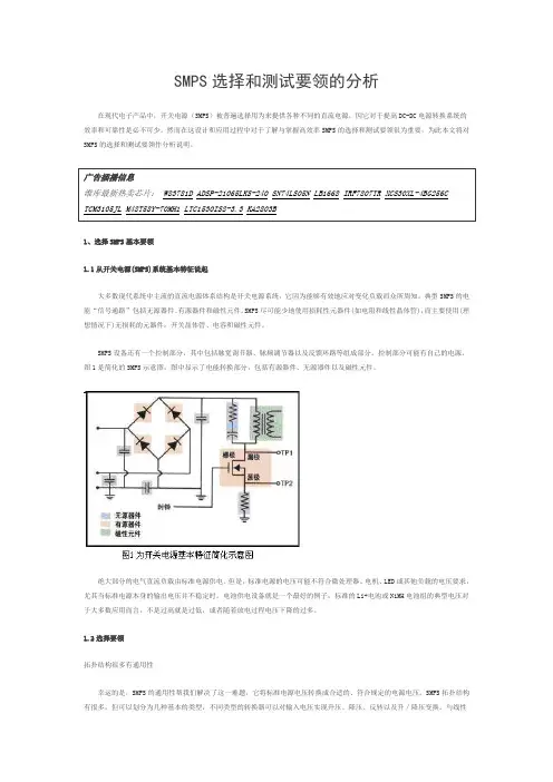
SMPS选择和测试要领的分析在现代电子产品中,开关电源(SMPS)被普遍选择用为来提供各种不同的直流电源,因它对于提高DC-DC电源转换系统的效率和可靠性是必不可少。
然而在这设计和应用过程中对于了解与掌握高效率SMPS的选择和测试要领很为重要,为此本文将对SMPS的选择和测试要领作分析说明。
1、选择SMPS基本要领1.1从开关电源(SMPS)系统基本特征说起大多数现代系统中主流的直流电源体系结构是开关电源系统,它因为能够有效地应对变化负载而众所周知。
典型SMPS的电能“信号通路”包括无源器件、有源器件和磁性元件。
SMPS尽可能少地使用损耗性元器件(如电阻和线性晶体管),而主要使用(理想情况下)无损耗的元器件:开关晶体管、电容和磁性元件。
SMPS设备还有一个控制部分,其中包括脉宽调节器、脉频调节器以及反馈环路等组成部分。
控制部分可能有自己的电源。
图1是简化的SMPS示意图,图中显示了电能转换部分,包括有源器件、无源器件以及磁性元件。
绝大部分的电气直流负载由标准电源供电。
但是,标准电源的电压可能不符合微处理器、电机、LED或其他负载的电压要求,尤其当标准电源本身的输出电压并不稳定时。
电池供电设备就是一个最好的例子:标准的Li+电池或NiMH电池组的典型电压对于大多数应用而言,不是过高就是过低,或者随着放电过程电压下降的过多。
1.2选择要领拓扑结构很多有通用性幸运的是,SMPS的通用性帮我们解决了这一难题,它将标准电源电压转换成合适的、符合规定的电源电压。
SMPS拓扑结构有很多,但可以划分为几种基本的类型,不同类型的转换器可以对输入电压实现升压、降压、反转以及升/降压变换。
与线性稳压器只能对输入电压进行降压不同的是,可以选择不同拓扑的SMPS来满足任何输出电压的需求,这也正是SMPS极具吸引力的原因。
如上所述,根据电路拓扑的不同,SMPS可以将(DC-DC)直流输入电压转换成不同的直流输出电压。
实际应用中存在多种拓扑结构,比较常见有三种非隔离式DC-DC拓扑结构,按照功能划分为:降压(buck 图2a所示)、升压(boost图2b所示)、升/降压(buck-boost或反转图2c所示)。
Linear 推出效率达98%的同步降压
凌力尔特公司推出效率非常高(达98%)的同步降压-升压型DC/DC 控制器LT8705,该器件可在输入电压高于、低于或等于输出电压的情况下运作。
这个器件用 4 个反馈环路来调节输入电流/ 电压以及输出电流/ 电压。
输入电流和电压反馈环路可防止太阳能电池过载。
输出电流环路为电池
充电器或电流源提供稳定的输出电流。
LT8705 可使用在多种应用中,例如电信和汽车中的电压稳定器、以及太阳能或高阻抗电源和电池系统。
LT8705 在 2.8V 至80V 的宽输入电压范围内工作,产生 1.3V 至80V 输出,采用单个电感器和 4 开关同步整流。
用单个器件可提供高达250W 的输出功率。
当多个电路并联时,可以实现更大的输出功率。
工作频率可在100kHz 至400kHz 范围内选择,也可同步至一个外部时钟。
LT8705 采用专有的电流模式控制架构,以降压或升压模式实现恒定频率工作,而且提供了
4 个强大的内置N 沟道MOSFET 栅极驱动器。
用户可以选择强制连续、断续和突发模式(Burst Mode®)工作,以最大限度地提高轻负载时的效率。
其他特点包括指示哪些反馈环路处于工作状态的伺服引脚、一个
3.3V/12mA LDO、可调软启动、内置芯片温度监视器、以及在-40 度C 至125 度C 的工作结温范围内准确度为±1% 的基准电压。
LT8705 采。
ltc3789芯片中文资料及推荐参数LTC3789 是一款高性能、降压-升压型开关稳压控制器,可以在输入电压高于、低于或等于输出电压的情况下运作。
该器件运用了恒定频率、电流模式架构,故可提供一个高达600kHz 的可锁相频率,而一个输出电流反馈环路则提供了对电池充电的支持。
凭借4V 至38V (最大值为40V)的宽输入和输出范围以及工作区之间的无缝和低噪声转换,LTC3789 成为了汽车、电信和电池供电型系统的理想选择。
在降压或升压模式时,LTC3789 运用专有电流模式控制架构实现恒定频率工作,而且内置了4 个强大的N 沟道MOSFET 栅极驱动器。
LTC3789 还提供一个准确的恒定电流调节环路,用于在宽输入电压范围内调节输入或输出电流。
输入电流限制功能防止输入电源过载,输出电流限制为诸如电池充电器或LED 驱动器等稳定输出电流应用提供了非常容易的解决方案。
该器件在所有工作模式下为过压、过流和短路情况提供了故障保护。
此外,LTC3789 在停机时断开输入电压和输出电压的连接。
用户可以选择连续或脉冲跳跃模式,以最大限度地提高轻负载效率,并允许将IC 同步至一个外部时钟。
脉冲跳跃模式在轻负载条件下可实现最低的纹波,而强制连续模式则工作于一个恒定的频率以满足噪声敏感型应用的需要。
此外,LTC3789 具有可调软启动、电源良好输出,并在-40C 至125C 的工作结温范围内保持1.5% 的基准电压准确度。
当输出位于其设计设定点的10% 以内时,一个电源良好输出引脚将发生指示信号。
LTC3789 采用扁平的28 引脚4mm x 5mm QFN 封装和窄体SSOP 封装。
LTC3789引脚说明LTC3789引脚图1. VFB(PIN1/PIN26):误差放大器反馈引脚。
LTC3789收到的反馈电压来自于外部电阻分压器输出的电压。
2. SS(PIN2/PIN27):外部软启动输入引脚。
LTC3789调节VFB电压到较小的0.8V或SS 引脚上的电压。
1LTC196823LTC1968456LTC1968INPUT FREQUENCY (kHz)02004001981002003005000.5%/DIV C AVE= 10µF V IN = 200mV RMS7LTC196889LTC1968101968fOutput ConnectionsThe LTC1968 output is differentially, but not symmetri-cally, generated. That is to say, the RMS value that the LTC1968 computes will be generated on the output (Pin 5)relative to the output return (Pin 6), but these two pins are not interchangeable. For most applications, Pin 6 will be tied to ground (Pin 1). However, Pin 6 can be tied to any voltage between 0V and V + (Pin 7) less the maximum output voltage swing desired. This last restriction keeps V OUT itself (Pin 5) within the range of 0V to V +. If a reference level other than ground is used, it should be a low impedance, both AC and DC, for proper operation of the LTC1968.In any configuration, the averaging capacitor should be connected between Pins 5 and 6. The LTC1968 RMS-DC output will be a positive voltage created at V OUT (Pin 5)with respect to OUT RTN (Pin 6).Power Supply BypassingThe LTC1968 is a switched capacitor device, and large transient power supply currents will be drawn as the switching occurs. For reliable operation, standard power supply bypassing must be included. A 0.01µF capacitor from V + (Pin 7) to GND (Pin 1) located close to the device will suffice. If there is a good quality ground plane avail-able, the capacitors can go directly to that instead. Power supply bypass capacitors can, of course, be inexpensive ceramic types.Up and Running!If you have followed along this far, you should have the LTC1968 up and running by now! Don’t forget to enable the device by grounding Pin 8, or driving it with a logic low.Keep in mind that the LTC1968 output impedance is fairly high, and that even the standard 10M Ω input impedance of a digital multimeter (DMM) or a 10× scope probe will load down the output enough to degrade its typical gain error of 0.1%. In the end application circuit, either a buffer or another component with an extremely high input imped-ance (such as a dual slope integrating ADC) should be used.APPLICATIO S I FOR ATIOW UUU For laboratory evaluation, it may suffice to use a bench-top DMM with the ability to disconnect the 10M Ω shunt.If you are still having trouble, it may be helpful to skip ahead a few pages and review the Troubleshooting Guide.What About Response Time?With a large value averaging capacitor, the LTC1968 can easily perform RMS-to-DC conversion on low frequency signals. It compares quite favorably in this regard to prior-generation products because nothing about the ∆Σcircuitry is temperature sensitive. So the RMS result doesn’t get distorted by signal driven thermal fluctuations like a log-antilog circuit output does.However, using large value capacitors results in a slow response time. Figure 10 shows the rising and falling step responses with a 10µF averaging capacitor. Although they both appear at first glance to be standard exponential-decay type settling, they are not. This is due to the nonlinear nature of an RMS-to-DC calculation. Also note the change in the time scale between the two; the rising edge is more than twice as fast to settle to a given accuracy. Again this is a necessary consequence of RMS-to-DC calculation.3Although shown with a step change between 0mV and 100mV, the same response shapes will occur with the LTC1968 for ANY step size. This is in marked contrast to prior generation log/antilog RMS-to-DC converters, whose averaging time constants are dependent on the signal level, resulting in excruciatingly long waits for the output to go to zero.The shape of the rising and falling edges will be dependent on the total percent change in the step, but for less than the 100% changes shown in Figure 10, the responses will be less distorted and more like a standard exponential decay.For example, when the input amplitude is changed from3 To convince oneself of this necessity, consider a pulse train of 50% duty cycle between 0mV and100mV. At very low frequencies, the LTC1968 will essentially track the input. But as the input frequency is increased, the average result will converge to the RMS value of the input. If the rise and fall characteristics were symmetrical, the output would converge to 50mV. In fact though, the RMS value of a 100mV DC-coupled 50% duty cycle pulse train is 70.71mV, which the asymmetrical rise and fall characteristics will converge to as the input frequency is increased.1968 F15 100ms/DIV1968 F14100ms/DIVFigure 15. Step Responses with 60Hz Burst Figure 14. Step Responses with 10Hz Burst1968fwaveform dynamics and the type of filtering used. The above method is conservative for some cases and about right for others.The LTC1968 works well with signals whose crest factor is 4 or less. At higher crest factors, the internal ∆Σmodulator will saturate, and results will vary depending on the exact frequency, shape and (to a lesser extent) ampli-tude of the input waveform. The output voltage could be higher or lower than the actual RMS of the input signal.The ∆Σ modulator may also saturate when signals with crest factors less than 4 are used with insufficient averag-ing. This will only occur when the output droops to less than 1/4 of the input voltage peak. For instance, a DC-coupled pulse train with a crest factor of 4 has a duty cycle of 6.25% and a 1V PEAK input is 250mV RMS . If this input is 50Hz, repeating every 20ms, and C AVE = 10µF, the output will droop during the inactive 93.75% of the waveform.This droop is calculated as:V V e MIN RMS INACTIVE TIME =⎛⎝⎜⎜⎞⎠⎟⎟−⎛⎝⎜⎞⎠⎟21– 2 • Z • C OUT AVE For the LTC1968, whose output impedance (Z OUT ) is12.5k Ω, this droop works out to –3.6%, so the output would be reduced to 241mV at the end of the inactive portion of the input. When the input signal again climbs to 1V PEAK , the peak/output ratio is 4.15.With C AVE = 100µF, the droop is only –0.37% to 249.1mV and the peak/output ratio is just 4.015, which the LTC1968has enough margin to handle without error.For crest factors less than 3.5, the selection of C AVE as previously described should be sufficient to avoid this droop and modulator saturation effect. B ut with crest factors above 3.5, the droop should also be checked for each design.Error AnalysesOnce the RMS-to-DC conversion circuit is working, it is time to take a step back and do an analysis of the accuracy of that conversion. The LTC1968 specifications include three basic static error terms, V OOS , V IOS and GAIN. The output offset is an error that simply adds to (or subtractsAPPLICATIO S I FOR ATIOW UUU from) the voltage at the output. The conversion gain of the LTC1968 is nominally 1.000 V DCOUT /V RMSIN and the gain error reflects the extent to which this conversion gain is not perfectly unity. Both of these affect the results in a fairly obvious way.Input offset on the other hand, despite its conceptual simplicity, effects the output in a nonobvious way. As its name implies, it is a constant error voltage that adds directly with the input. And it is the sum of the input and V IOS that is RMS converted.This means that the effect of V IOS is warped by the nonlinear RMS conversion. With 0.4mV (typ) V IOS , and a 200mV RMS AC input, the RMS calculation will add the DC and AC terms in an RMS fashion and the effect is negligible:V OUT = √(200mV AC)2 + (0.4mV DC)2= 200.0004mV = 200mV + 2ppmBut with 10× less AC input, the error caused by V IOS is 100× larger:V OUT = √(20mV AC)2 + (0.4mV DC)2= 20.004mV= 20mV + 200ppmThis phenomena, although small, is one source of the LTC1968’s residual nonlinearity.On the other hand, if the input is DC coupled, the input offset voltage adds directly. With +200mV and a +0.4mV V IOS , a 200.4mV output will result, an error of 0.2% or 2000ppm. With DC inputs, the error caused by V IOS can be positive or negative depending if the two have the same or opposing polarity.The total conversion error with a sine wave input using the typical values of the LTC1968 static errors is computed as follows:V OUT = (√(500mV AC)2 + (0.4mV DC)2) • 1.001 + 0.2mV= 500.700mV= 500mV + 0.140%V OUT = (√(50mV AC)2 + (0.4mV DC)2) • 1.001 + 0.2mV= 50.252mV= 50mV + 0.503%211968fAPPLICATIO S I FOR ATIOW UUU This allows each sample to settle to within 46ppm and it is these samples that are used to compute the RMS value.This is a much higher accuracy than the LTC1968 conver-sion limits, and far better than the accuracy computed via the simplistic resistive divider model:Output ImpedanceThe LTC1968 output impedance during operation is simi-larly due to a switched capacitor action. In this case, 20pF of on-chip capacitance operating at 2MHz translates into 25k Ω. The closed-loop RMS-to-DC calculation cuts that in half to the nominal 12.5k Ω specified.In order to create a DC result, a large averaging capacitor is required. Capacitive loading and time constants are not an issue on the output.However, resistive loading is an issue and the 10M Ωimpedance of a DMM or 10× scope probe will drag the output down by –0.125% typ.During shutdown, the switching action is halted and a fixed 12.5k resistor shunts V OUT to OUT RTN so that C AVE is discharged.Interfacing with an ADCThe LTC1968 output impedance and the RMS averaging ripple need to be considered when using an analog-to-digital converter (ADC) to digitize the LTC1968 RMS result.The simplest configuration is to connect the LTC1968directly to the input of a type 7106/7136 ADC as shown in Figure 21a. These devices are designed specifically for DVM/DPM use and include display drivers for a 3 1/2 digit LCD segmented display. Using a dual-slope conversion,the input is sampled over a long integration window, which results in rejection of line frequency ripple when integra-tion time is an integer number of line cycles. Finally, these parts have an input impedance in the G Ω range, with specified input leakage of 10pA to 20pA. Such a leakage,combined with the LTC1968 output impedance, results in less than 1µV of additional output offset voltage.Another type of ADC that has inherent rejection of RMS averaging ripple is an oversampling ∆Σ ADC such as the LTC2420. Its input impedance is 6.5M Ω, but only when it is sampling. Since this occurs only half the time at most,if it directly loads the LTC1968, a gain error of –0.08% to –0.11% results. In fact, the LTC2420 DC input current isV V R R R V M V IN SOURCEININ SOURCESOURCESOURCE =+=Ω= 1.2125–.%M k Ω+1.215.5ΩThis resistive divider calculation does give the correct model of what voltage is seen at the input terminals by a parallel load averaged over a several clock cycles, which is what a large shunt capacitor will do—average the current spikes over several clock cycles.When high source impedances are used, care must be taken to minimize shunt capacitance at the LTC1968 input so as not to increase the settling time. Shunt capacitance of just 0.8pF will double the input settling time constant and the error in the above example grows from 46ppm to 0.67%(6700ppm). As a consequence, it is important to not try to filter the input with large input capacitances unless driven by a low impedance. Keep time constant <<125ns.When the LTC1968 is driven by op amp outputs, whose low DC impedance can be compromised by sharp capaci-tive load switching, a small series resistor may be added.A 1k resistor will easily settle with the 0.8pF input sampling capacitor to within 1ppm.These are important points to consider both during design and debug. During lab debug, and even production testing,a high value series resistor to any test point is advisable.22231968fThe trade-off here is that on the one hand, the DC error is input frequency dependent, so a calibration signal fre-quency high enough to make the DC error negligible should be used. On the other hand, as low a frequency as can be used is best to avoid attenuation of the calibrated AC signal, either from parasitic RC loading or insufficient op amp gain. For instance, with a 1kHz calibration signal,a 1MHz op amp will typically only have 60dB of open-loop gain, so it could attenuate the calibration signal a full 0.1%.AC-Only, 2 PointThe next most significant error for AC-coupled applica-tions will be the effect of output offset voltage, noticeable at the bottom end of the input scale. This too can be calibrated out if two measurements are made, one with a full-scale sine wave input and a second with a sine wave input (of the same frequency) at 10% of full scale. The trade-off in selecting this second level is that it should be small enough that the gain error effect becomes small compared to the gain error effect at full scale, while on the other hand, not using so small an input that the input offset voltage becomes an issue.The calculations of the error terms for a 200mV full-scale case are:Gain =Reading at 200mV –Reading at 20mV180mV Output Offset =Reading at 20mVGain–20mVDC, 2 PointDC-based calibration is preferable in many cases because a DC voltage of known, good accuracy is easier to gener-ate than such an AC calibration voltage. The only down side is that the LTC1968 input offset voltage plays a role.It is therefore suggested that a DC-based calibration scheme check at least two points: ±full scale. Applying the–full-scale input can be done by physically inverting the voltage or by applying the same +full-scale input to the opposite LTC1968 input.For an otherwise AC-coupled application, only the gain term may be worth correcting for, but for DC-coupled applications, the input offset voltage can also be calcu-lated and corrected for.The calculations of the error terms for a 200mV full-scale case are:Gain =Reading at 200mV +Reading at –200mV400mV Input Offset =Reading at –200mV –Reading at 200mV2•GainNote: Calculation of and correction for input offset voltage are the only way in which the two LTC1968 inputs (IN1,IN2) are distinguishable from each other. The calculation above assumes the standard definition of offset; that a positive offset is the case of a positive voltage error inside the device that must be corrected by applying a like negative voltage outside. The offset is referred to which-ever pin is driven positive for the +full-scale reading.DC, 3 PointOne more point is needed with a DC calibration scheme to determine output offset voltage: +10% of full scale.The calculation of the input offset is the same as for the 2-point calibration above, while the gain and output offset are calculated for a 200mV full-scale case as:Gain =Reading at 200mV –Reading at 20mV180mV Output Offset =Reading at 200mV +Reading at –200mV –400mV •Gain2APPLICATIO S I FOR ATIOW UUU24252627Information furnished by Linear Technology Corporation is believed to be accurate and reliable.However, no responsibility is assumed for its use. Linear Technology Corporation makes no represen-tation that the interconnection of its circuits as described herein will not infringe on existing patent rights.VOLTAGE NOISE IN28© LINEAR TECHNOLOGY CORPORA TION 2004LT/TP 0604 1K • PRINTED IN USALinear Technology Corporation1630 McCarthy Blvd., Milpitas, CA 95035-7417(408) 432-1900 ● FAX: (408) 434-0507 ● 。
新闻发布 40V IN/OUT、2A 同步降压-升压型 DC/DC 转换器提供 2.7V 至 40V 的输入和输出范围加利福尼亚州米尔皮塔斯 (MILPITAS, CA) – 2011 年 11 月 21 日– 凌力尔特公司(Linear Technology Corporation) 推出同步降压-升压型转换器LTC3115-1 ,该器件可使用从单节锂离子电池、24V/28V工业电源轨到 40V 汽车输入的多种电源,提供高达 2A 的连续输出电流。
LTC3115-1 具 2.7V 至 40V 的输入和输出范围,在输入高于、低于或等于输出时,可提供稳定的输出。
LTC3115-1 采用的低噪声降压-升压型拓扑在降压和升压模式之间提供连续和无抖动转换,从而非常适用于 RF 以及其他噪声敏感型应用,这类应用在使用可变输入电源时,必须保持低噪声恒定输出电压。
在许多应用中,相比于专门的降压型解决方案,这款器件可显著延长电池的运行时间。
LTC3115-1 的开关频率范围为 100kHz 至 2MHz,是用户可编程的,并可同步至一个外部时钟。
专有的第三代降压-升压型 PWM 电路确保低噪声和高效率,同时最大限度地减小了外部组件的尺寸。
纤巧的外部组件与 4mm x 5mm DFN 或 TSSOP-20E 封装相结合,可组成占板面积紧凑的解决方案。
LTC3115-1 采用 4 个内部低 R DS(ON) N 沟道 MOSFET,以提供高达 95% 的效率。
用户可选的突发模式 (Burst Mode®) 工作使静态电流降至仅为 50uA,从而提高了轻负载效率,并延长了电池运行时间。
就噪声敏感型应用而言,可禁止突发模式工作。
其他特点包括内部软启动、可编程欠压保护、短路保护以及输出断接。
LTC3115EDHD-1 采用 16 引线 4mm x 5mm DFN 封装,LTC3115EFE-1 采用耐热增强型 20 引线 TSSOP 封装。
电磁辐射 (EMR)、电磁干扰 (EMI) 和电磁兼容性 (EMC) 是涉及来自带电粒子的能量以及可能干扰电路性能和信号传输的相关磁场的术语。
随着无线通信的激增,通信装置不计其数,再加上越来越多的通信方法 (包括蜂窝、Wi-Fi、卫星、GPS 等) 使用的频谱越来越多 (有些频带相互重叠),电磁干扰成了客观存在的事实。
为了减轻此影响,许多政府机构和监管组织对通信装置、设备和仪器可发射的辐射量设定了限制。
这类规范的示例之一是 CISPR 16-1-3,它涉及无线电干扰和抗扰度测量设备和测量方法。
根据其特征,电磁干扰可分为传导干扰 (通过电源传输) 或辐射干扰 (通过空气传输)。
开关电源会产生两种类型的干扰。
ADI 公司为减少传导干扰和辐射干扰实施的一项技术是扩频频率调制 (SSFM)。
该技术用于我们一些基于电感和电容的开关电源、硅振荡器和 LED 驱动器,将噪声扩展到更宽的频带上,从而降低特定频率下的峰值噪声和平均值噪声。
SSFM 不允许发射能量在任何接收器的频带中停留过长时间,从而改善了EMI。
有效 SSFM的关键决定因素是频率扩展量和调制速率。
对于开关稳压器应用来说,典型扩展量为 ±10%,最佳调制速率取决于调制方式。
SSFM 可采用各种频率扩展方法,例如使用正弦波或三角波调制时钟频率。
调制方法大多数开关稳压器都会呈现与频率相关的纹波:开关频率越低则纹波越多,开关频率越高则纹波越少。
因此,如果对开关时钟进行频率调制,则开关稳压器的纹波将呈现幅度调制。
如果时钟的调制信号是周期性的 (例如正弦波或三角波),则将呈现周期性的纹波调制,而且在调制频率上存在一个明显的频谱分量 (图 1)。
图 1.由时钟的正弦波频率调制引起的开关稳压器纹波图解。
由于调制频率远低于开关稳压器的时钟频率,因此可能难以滤除。
由于下游电路中的电源噪声耦合或有限的电源抑制,这可能导致可听音或明显的伪像等问题。
伪随机频率调制能够消除这种周期性纹波。
LED升压、升降压的驱动恒流IC推荐二美国美信集成产品公司MAX16831 可配置升降压型高功率LED 驱动IC MAX16831 是一款电流型、高亮LED(HBLED)驱动器,设计为通过控制2 个外部n 沟道MOSFET 来调节单串LED 的电流。
MAX16831 集成了宽范围亮度控制、固定频率HBLED 驱动器所需的全部组件。
MAX16831 可配置为降压型(buck)、升压型(boost)或升/降压型(buck-boost)电流调节器。
带有前沿消隐的电流模式简化了控制回路的设计。
内部斜率补偿可在占空比超过50%时保持电流环路的稳定。
MAX16831 工作于较宽的输入电压范围,并可承受汽车抛负载事件。
多个MAX16831 可相互同步或同步至外部时钟。
MAX16831 包含一个浮动亮度驱动器,驱动串联在LED 串的n 沟道MOSFET 实现亮度控制。
使用MAX16831 架构的HBLED 驱动器可在汽车应用中实现超过90%的效率。
MAX16831 还包括一个可源出1.4A、吸收2.5A 电流(sink)的栅极驱动器,用于在高功率LED 驱动器应用中驱动开关MOSFET,如车灯总成等。
亮度控制允许宽范围的PWM 调光,其频率可高达2kHz。
在较低的调光频率下可实现高达1000:1 的调光比。
MAX16831 提供带裸焊盘的32 引脚薄型QFN 封装,工作于-40°C至+125°C 汽车级温基本参数:宽输入范围:6V 至76V;集成LED 电流检测差分放大器;可驱动n 沟道MOSFET;具有浮动亮度驱动能力;LED 电流精度:5%;200Hz 片上斜坡发生器,可同步至外部PWM 亮度信号;可编程开关频率(125kHz 至600kHz),可被同步;输出过压、负载开路、LED 短路、过热保护;低至107mV LED 电流检。
1LTC344223442fV IN , V OUT Voltage...........................................–0.3 to 6V SW1, SW2 VoltageDC .................................................................–0.3 to 6V Pulsed <100ns...............................................–0.3 to 7V SHDN/SS, BURST Voltage.............................–0.3 to 6V Operating Temperature (Note 2).............–40°C to 85°C Maximum Junction Temperature (Note 4)............125°C Storage Temperature Range.................–65°C to 125°CORDER PART NUMBER DE PART MARKING 3442LTC3442EDEABSOLUTE AXI U RATI GSW W WU PACKAGE/ORDER I FOR ATIOUUW (Note 1)ELECTRICAL CHARACTERISTICSThe ● denotes the specifications which apply over the full operatingtemperature range, otherwise specifications are at T A = 25°C. V IN = V OUT = 3.6V, R T = 64.9k, unless otherwise noted.PARAMETER CONDITIONSMIN TYP MAX UNITSInput Start-Up Voltage ● 2.3 2.4V Output Voltage Adjust Range ● 2.4 5.25V Feedback Voltage ●1.191.22 1.25V Feedback Input CurrentV FB = 1.22V150nA Quiescent Current – Burst Mode Operation V FB = 1.22V, BURST = 0V (Note 3)3560µA Quiescent Current – Shutdown SHDN = 0V, V OUT = 0V, Not Including Switch Leakage 0.11µA Quiescent Current – Active BURST = V IN (Note 3)6001100µA NMOS Switch Leakage Switches B and C 0.12µA PMOS Switch Leakage Switches A and D 0.13µA NMOS Switch On Resistance Switches B and C 0.10ΩPMOS Switch On Resistance Switches A and D0.10ΩInput Current Limit ●23A Reverse Current Limit0.5A Burst Mode Operation Current Limit 0.9A Max Duty Cycle Boost (% Switch C On)●7088%Buck (% Switch A In)●100 %Min Duty Cycle ●0%Frequency Accuracy ●570670770kHz Error Amp A VOL90dB Error Amp Source Current 11µA Error Amp Sink Current 300µA Burst Threshold (Falling)0.88V Burst Threshold (Rising)1.12VT JMAX = 125°CθJA = 53°C/W 1-Layer Board θJA = 43°C/W 4-Layer BoardθJC = 4.3°C/WEXPOSED PAD IS PGND (PIN 13)MUST BE SOLDERED TO PCB121110987123456FB V C R LIM V IN V OUT BURSTSHDN/SSRT SGND SW1PGND SW2TOP VIEW13DE12 PACKAGE12-LEAD (4mm × 3mm) PLASTIC DFN350ns/DIV3442 G15V IN = 2.9VV OUT = 3.3V AT 500mA4LTC344253442f200µs/DIV3442 G22C OUT = 100µFLOW ESR TANTALUMINDUCTOR CURRENT 0.5A/DIVV OUT 50mV/DIV1ms/DIV3442 G23R LIM = 133k C LIM = .001µFINDUCTOR CURRENT 0.5A/DIVR LIM PIN 0.5V/DIV VOUT 2V/DIV20µs/DIV3442 G21C OUT = 100µFLOW ESR TANTALUMINDUCTOR CURRENT 0.5A/DIVV OUT 50mV/DIV50ns/DIV3442 G17SW12V/DIVSW22V/DIVV IN = 4.2VVOUT = 3.3V AT 500mA50ns/DIV3442 G16SW12V/DIV SW22V/DIVV IN = 3.3VV OUT = 3.3V AT 500mATYPICAL PERFOR A CE CHARACTERISTICS U WSwitch Pins in Buck-Boost ModeSwitch Pins Entering Buck-Boost ModeOutput Ripple at 1A LoadLoad Transient Response in Fixed Frequency Mode, No Load to 1ALoad Transient Response in Auto Burst Mode Operation, No Load to 1ABurst Mode OperationPulsed Overload Using Average Input Current LimitTransition from Burst ModeOperation to Fixed Frequency Mode1µs/DIV3442 G18V OUT20mV/DIV AC COUPLEDV IN = 4.2VV IN = 3.3VV IN = 2.7V 100µs/DIV3442 G19V IN = 3.6V V OUT = 3.3VC OUT = 47µF, X5R CERAMICLOAD 0.5A/DIVVOUT 100mV/DIV100µs/DIV3442 G20V IN = 3.6V V OUT = 3.3VC OUT = 47µF, X5R CERAMIC + 100µF LOW ESR TANTALUMLOAD 0.5A/DIVV OUT 100mV/DIV(T A = 25°C unless otherwise specified).LTC344263442fU U UPI FU CTIO SSHDN/SS (Pin 1): Combined Soft-Start and Shutdown.Applied voltage <0.4V shuts down the IC. Tie to >1.4V to enable the IC and >2.4V to ensure the error amp is not clamped from soft-start. An RC network from the shut-down command signal to this pin will provide a soft-start function by limiting the rise time of the V C pin.R T (Pin 2): Programs the Frequency of the Internal Oscil-lator. Place a resistor from this pin to ground. See the Applications Information section for component value selection.SGND (Pin 3): Signal Ground for the IC.SW1 (Pin 4): Switch Pin Where Internal Switches A and B are Connected. Connect inductor from SW1 to SW2. An optional Schottky diode can be connected from SW1 to ground for a moderate efficiency improvement. Minimize trace length to reduce EMI.PGND (Pin 5, 13): Power Ground for the Internal NMOS Power Switches. The exposed pad must be soldered to PCB ground to provide both electrical contact and a good thermal contact to the PCB.SW2 (Pin 6): Switch Pin Where Internal Switches C and D are Connected. An optional Schottky diode can be con-nected from SW2 to V OUT for a moderate efficiency im-provement. Minimize trace length to reduce EMI.BURST (Pin 7): Used to set the Automatic Burst Mode Operation Threshold. Place a resistor and capacitor in parallel from this pin to ground. See the Applications Information section for component value selection. For manual control, ground the pin to force Burst Mode operation, connect to V OUT to force fixed frequency mode.V OUT (Pin 8): Output of the Synchronous Rectifier. A filter capacitor is placed from V OUT to GND. A ceramic bypass capacitor is recommended as close to the V OUT and GND pins as possible.V IN (Pin 9): Input Supply Pin. Internal V CC for the IC. A 10µF ceramic capacitor is recommended as close to V IN and SGND as possible.R LIM (Pin 10): Sets the Average Input Current Limit Threshold. Place a resistor and capacitor in parallel from this pin to ground. See the Applications Information section for component value selection.V C (Pin 11): Error Amp Output. A frequency compensation network is connected from this pin to FB to compensate the loop. During Burst Mode operation, V C is internally connected to a hold circuit.FB (Pin 12): Feedback Pin. Connect resistor divider tap here. The output voltage can be adjusted from 2.4V to 5.25V. The feedback reference voltage is typically 1.22V.7LTC344283442fThe LTC3442 provides high efficiency, low noise power for applications such as portable instrumentation. The LTC proprietary topology allows input voltages above,below or equal to the output voltage by properly phasing the output switches. The error amp output voltage on V C determines the output duty cycle of the switches. Since V C is a filtered signal, it provides rejection of frequencies from well below the switching frequency. The low R DS(ON),low gate charge synchronous switches provide high frequency pulse width modulation control at high effi-ciency. Schottky diodes across the synchronous switch D and synchronous switch B are not required, but provide a lower voltage drop during the break-before-make time (typically 15ns). Schottky diodes will improve peak effi-ciency by typically 1% to 2%. High efficiency is achieved at light loads when Burst Mode operation is entered and the IC’s quiescent current drops to a low 35µA.LOW NOISE FIXED FREQUENCY OPERATION OscillatorThe frequency of operation is programmed by an external resistor from R T to ground, according to the following equation:f R kHz T k ()(),=Ω43300Error AmpThe error amplifier is a voltage mode amplifier. The loop compensation components are configured around the amplifier (from FB to V C ) to obtain stability of the con-verter. For improved bandwidth, an additional RC feed-forward network can be placed across the upper feedback divider resistor. The voltage on SHDN/SS clamps the error amp output, V C , to provide a soft-start function.OPERATIOUInternal Current LimitThere are three different current limit circuits in the LTC3442. Two have internally fixed thresholds which vary inversely with V IN , the third is externally programmable,and does not vary with input voltage.The first circuit is a high speed peak current limit amplifier that will shut off switch A if the current exceeds 5A typical.The delay to output of this amplifier is typically 50ns.A second amplifier will begin to source current into the FB pin to drop the output voltage once the peak input current exceeds 3A typical. This method provides a closed loop means of clamping the input current. During conditions where V OUT is near ground, such as during a short-circuit or during startup, this threshold is cut in half, providing a foldback feature. For this current limit feature to be most effective, the Thevenin resistance from FB to ground should be greater than 100k Ω.Externally Programmable Current LimitThe third current limit circuit is programmed by an exter-nal resistor on R LIM . This circuit works by mirroring the input current in switch A, averaging it by means of the external RC network on R LIM , and comparing the resulting voltage with an internal reference. If the voltage on R LIM starts to exceed 0.95V, a G m amplifier will clamp V C ,lowering V OUT to maintain control of the input current.This allows the user to program a maximum average input current, for applications such as USB, where the current draw from the bus must be limited to 500mA. The resistor and capacitor values are determined by the following equations:R V V I C R LIM k IN OUT IN AMPS LIM F LIM k ()()()()•.•–.ΩµΩ=+()⎛⎝⎜⎜⎞⎠⎟⎟≥7008624001910LTC3442113442fcurrent in Amps. Do not use values of R BURST greater than 250k.For automatic operation, a filter capacitor should also be connected from BURST to ground to prevent ripple on BURST from causing the IC to oscillate in and out of Burst Mode operation. The equation for the minimum capacitor value is:C C V BURST MIN OUT OUT ()•,≥60000where C BURST(MIN) and C OUT are in µFIn the event that a load transient causes the feedback pin to drop by more than 4% from the regulation value while in Burst Mode operation, the IC will immediately switch to fixed frequency mode and an internal pull-up will be momentarily applied to BURST, rapidly charging the BURST cap. This prevents the IC from immediately re-entering Burst Mode operation once the output achieves regulation.Manual Burst Mode OperationFor manual control of Burst Mode operation, the RC network connected to BURST can be eliminated. To force fixed frequency mode, BURST should be connected to V OUT . To force Burst Mode operation, BURST should be grounded. When commanding Burst Mode operation manually, the circuit connected to BURST should be able to sink up to 2mA.For optimum transient response with large dynamic loads,the operating mode should be controlled manually by the host. By commanding fixed frequency operation prior to a sudden increase in load, output voltage droop can be minimized. Note that if the load current applied during forced Burst Mode operation (BURST pin is grounded)exceeds the current that can be supplied, the output voltage will start to droop and the IC will automatically come out of Burst Mode operation and enter fixed fre-quency mode, raising V OUT . Once regulation is achieved,the IC will then enter Burst Mode operation once again,and the cycle will repeat, resulting in about 4% output ripple. Note that Burst Mode operation is inhibited during soft-start.Burst Mode Operation to Fixed Frequency Transient ResponseIn Burst Mode operation, the compensation network is not used and V C is disconnected from the error amplifier.During long periods of Burst mode operation, leakage currents in the external components or on the PC board could cause the compensation capacitor to charge (or discharge), which could result in a large output transient when returning to fixed frequency mode of operation, even at the same load current. To prevent this, the LTC3442incorporates an active clamp circuit that holds the voltage on V C at an optimal voltage during Burst Mode operation.This minimizes any output transient when returning to fixed frequency mode operation. For optimum transientOPERATIOU1213LTC3442143442fTable 2. Capacitor Vendor InformationSUPPLIER PHONE FAXWEB SITE AVX (803) 448-9411(803) Murata (814) 237-1431(814) (800) 831-9172Sanyo (619) 661-6322(619) Taiyo Yuden (408) 573-4150(408) TDK(847) 803-6100(847) 803-6296voltages as low as 0.4V. The part is specified at 2.4V minimum to allow operation without the requirement of a Schottky diode. Synchronous switch D is powered from V OUT and the R DS(ON) will increase at low output voltages,therefore a Schottky diode is required from SW2 to V OUT to provide the conduction path to the output. Note that Burst Mode operation is inhibited at output voltages below 1.6V typical.Output Voltage > 4.3VA Schottky diode from SW2 to V OUT is required for output voltages over 4.3V. The diode must be located as close to the pins as possible in order to reduce the peak voltage on SW2 due to the parasitic lead and trace inductance.Input Voltage > 4.5VFor applications with input voltages above 4.5V which could exhibit an overload or short-circuit condition, a 2Ω/1nF series snubber is required between SW1 and GND. A Schottky diode from SW1 to V IN should also be added as close to the pins as possible. For the higher input voltages, V IN bypassing becomes more critical; therefore,a ceramic bypass capacitor as close to the V IN and SGND pins as possible is also required.Operating Frequency SelectionHigher operating frequencies allow the use of a smaller inductor and smaller input and output filter capacitors,thus reducing board area and component height. How-ever, higher operating frequencies also increase the IC’s total quiescent current due to the gate charge of the four switches, as given by:Buck:Iq = (0.8 • V IN • f) mA Boost:Iq = [0.4 • (V IN + V OUT ) • f] mABuck/Boost:Iq = [f • (1.2 • V IN + 0.4 • V OUT )] mAThe output capacitance is usually many times larger than the minimum value in order to handle the transient re-sponse requirements of the converter. For a rule of thumb,the ratio of the operating frequency to the unity-gain bandwidth of the converter is the amount the output capacitance will have to increase from the above calcula-tions in order to maintain the desired transient response.The other component of ripple is due to the ESR (equiva-lent series resistance) of the output capacitor. Low ESR capacitors should be used to minimize output voltage ripple. For surface mount applications, Taiyo Yuden or TDK ceramic capacitors, AVX TPS series tantalum capaci-tors or Sanyo POSCAP are recommended. See Table 2 for contact information.Input Capacitor SelectionSince V IN is the supply voltage for the IC, as well as the input to the power stage of the converter, it is recom-mended to place at least a 4.7µF, low ESR ceramic bypass capacitor close to the V IN and SGND pins. It is also important to minimize any stray resistance from the con-verter to the battery or other power source.Optional Schottky DiodesThe Schottky diodes across the synchronous switches B and D are not required (V OUT < 4.3V), but provide a lower drop during the break-before-make time (typically 15ns)improving efficiency. Use a surface mount Schottky diode such as an MBRM120T3 or equivalent. Do not use ordi-nary rectifier diodes, since the slow recovery times will compromise efficiency. For applications with an output voltage above 4.3V, a Schottky diode is required from SW2 to V OUT .Output Voltage < 2.4VThe LTC3442 can operate as a buck converter with outputAPPLICATIO S I FOR ATIOW UUU–+1516171819Information furnished by Linear Technology Corporation is believed to be accurate and reliable.However, no responsibility is assumed for its use. Linear Technology Corporation makes no represen-tation that the interconnection of its circuits as described herein will not infringe on existing patent rights.LTC3442203442fLinear Technology Corporation1630 McCarthy Blvd., Milpitas, CA 95035-7417(408) 432-1900 ● FAX: (408) 434-0507 ● © LINEAR TECHNOLOGY CORPORA TION 2004LT/TP 1204 1K • PRINTED IN USARELATED PARTSPART NUMBER DESCRIPTIONCOMMENTSLT ®1613550mA (I SW ), 1.4MHz, High Efficiency Step-Up DC/DC Converter V IN : 0.9V to 10V, V OUT(MAX) = 34V, I Q = 3mA,I SD < 1µA, ThinSOT TM PackageLT1618 1.5A (I SW ), 1.25MHz, High Efficiency Step-Up DC/DC Converter V IN : 1.6V to 18V, V OUT(MAX) = 35V, I Q = 1.8mA,I SD < 1µA, MS10 PackageLT1930/LT1930A 1A (I SW ), 1.2MHz/2.2MHz, High Efficiency Step-Up DC/DC Converter V IN : 2.6V to 16V, V OUT(MAX) = 34V,I Q = 4.2mA/5.5mA, I SD < 1µA, ThinSOT Package LT19352A (I SW ), 1.2MHz, 38V Step-Up DC/DC Converter V IN : 2.3V to 16V, V OUT(MAX) = 38V, I Q = 3mA,I SD < 1µA, ThinSOT PackageLT1946/LT1946A 1.5A (I SW ), 1.2MHz/2.7MHz, High Efficiency Step-Up V IN : 2.45V to 16V, V OUT(MAX) = 34V, I Q = 3.2mA,DC/DC ConverterI SD < 1µA, MS8 PackageLT19611.5A (I SW ), 1.25MHz, High Efficiency Step-Up DC/DC ConverterV IN : 3V to 25V, V OUT(MAX) = 35V, I Q = 0.9mA,I SD = 6µA, MS8E PackageLTC3400/LTC3400B 600mA (I SW ), 1.2MHz Synchronous Step-Up DC/DC Converter V IN : 0.85V to 5V, V OUT(MAX) = 5V,I Q = 19µA/300µA, I SD < 1µA, ThinSOT Package LTC3401/LTC34021A/2A (I SW ), 3MHz Synchronous Step-Up DC/DC ConverterV IN : 0.5V to 5V, V OUT(MAX) = 6V, I Q = 38µA,I SD < 1µA, MS PackageLTC3405/LTC3405A 300mA (I OUT ), 1.5MHz Synchronous Step-Down DC/DC Converter V IN : 2.7V to 6V, V OUT(MIN) = 0.8V, I Q = 20µA,I SD ≤ 1µA, MS10 PackageLTC3406/LTC3406B 600mA (I OUT ), 1.5MHz Synchronous Step-Down DC/DC Converter V IN : 2.5V to 5.5V, V OUT(MIN) = 0.6V, I Q = 20µA,I SD ≤ 1µA, ThinSOT PackageLTC3407600mA (I OUT ), 1.5MHz Dual Synchronous Step-Down V IN : 2.5V to 5.5V, V OUT(MIN) = 0.6V, I Q = 40µA,DC/DC ConverterI SD ≤ 1µA, MS PackageLTC3411 1.25A (I OUT ), 4MHz Synchronous Step-Down DC/DC Converter V IN : 2.5V to 5.5V, V OUT(MIN) = 0.8V, I Q = 60µA,I SD ≤ 1µA, MS PackageLTC3412 2.5A (I OUT ), 4MHz Synchronous Step-Down DC/DC Converter V IN : 2.5V to 5.5V, V OUT(MIN) = 0.8V, I Q = 60µA,I SD ≤ 1µA, TSSOP16E PackageLTC34213A (I SW ), 3MHz Synchronous Step-Up DC/DC Converter V IN : 0.5V to 4.5V, V OUT(MAX) = 5.25V, I Q = 12µA,I SD < 1µA, QFN PackageLTC34255A (I SW ), 8MHz Multiphase Synchronous Step-Up V IN : 0.5V to 4.5V, V OUT(MAX) = 5.25V, I Q = 12µA,DC/DC ConverterI SD < 1µA, QFN PackageLTC3429600mA (I SW ), 500kHz Synchronous Step-Up DC/DC Converter V IN : 0.5V to 4.4V, V OUT(MIN) = 5V, I Q = 20µA,I SD < 1µA, QFN PackageLTC34363A (I SW ), 1MHz, 34V Step-Up DC/DC ConverterV IN : 3V to 25V, V OUT(MAX) = 34V, I Q = 0.9mA,I SD < 6µA, TSSOP-16E PackageLTC3440600mA (I OUT ), 2MHz Synchronous Buck-Boost DC/DC Converter V IN : 2.5V to 5.5V, V OUT(MIN) = 5.5V, I Q = 25µA,I SD < 1µA, MS, DFN PackagesLTC3441600mA (I OUT ), 2MHz Synchronous Buck-Boost DC/DC Converter V IN : 2.5V to 5.5V, V OUT(MIN) = 5.5V, I Q = 25µA,I SD < 1µA, DFN PackageLTC3443 1.2A (I OUT ), 600kHz Synchronous Buck-Boost DC/DC Converter V IN : 2.4V to 5.5V, V OUT(MIN) = 5.25V, I Q = 28µA,I SD < 1µA, MS PackageLT34671.1A (I SW ), 1.3MHz, High Efficiency Step-Up DC/DC ConverterV IN : 2.6V to 16V, V OUT(MAX) = 40V, I Q = 1.2mA,I SD < 1µA, ThinSOT PackageThinSOT is a trademark of Linear Technology Corporation.。
1LTC34412sn3441 3441fsV IN , V OUT Voltage........................................ –0.3V to 6V SW1, SW2 VoltageDC ...........................................................–0.3V to 6V Pulsed < 100ns ...................................... –0.3V to 7V SHDN/SS, MODE/SYNC Voltage................. –0.3V to 6V Operating Temperature Range (Note 2)..–40°C to 85°C Maximum Junction Temperature (Note 4)........... 125°C Storage Temperature Range................ –65°C to 125°CORDER PART NUMBER (Note 1)ABSOLUTE AXI U RATI GSW W WU PACKAGE/ORDER I FOR ATIOU U WConsult LTC Marketing for parts specified with wider operating temperature ranges.LTC3441EDET JMAX = 125°CθJA = 53°C/W 1-LAYER BOARD θJA = 43°C/W 4-LAYER BOARDθJC = 4.3°C/WEXPOSED PAD IS PGND (PIN 13)MUST BE SOLDERED TO PCBDE PART MARKING3441121110987123456FB V C V IN PV IN V OUT MODE/SYNCSHDN/SSGND PGND SW1SW2PGNDTOP VIEW13DE12 PACKAGE12-LEAD (4mm × 3mm) PLASTIC DFN The ● denotes the specifications which apply over the full operatingtemperature range, otherwise specifications are at T A = 25°C. V IN = V OUT = 3.6V,unless otherwise noted.ELECTRICAL CHARACTERISTICSPARAMETER CONDITIONSMINTYP MAX UNITSInput Start-Up Voltage ● 2.32.4V Output Voltage Adjust Range ● 2.4 5.25V Feedback Voltage ●1.191.22 1.25V Feedback Input CurrentV FB = 1.22V 150nA Quiescent Current—Burst Mode Operation V C = 0V, MODE/SYNC = 3V (Note 3)2540µA Quiescent Current—SHDN V OUT = SHDN = 0V, Not Including Switch Leakage 0.11µA Quiescent Current—Active MODE/SYNC = 0V (Note 3)520900µA NMOS Switch Leakage Switches B and C 0.17µA PMOS Switch Leakage Switches A and D 0.110µA NMOS Switch On Resistance Switches B and C 0.10ΩPMOS Switch On Resistance Switches A and D0.11ΩInput Current Limit ●2 3.2A Max Duty Cycle Boost (% Switch C On)●7088%Buck (% Switch A In)●100%Min Duty Cycle ●0%Frequency Accuracy ●0.8511.15MHz MODE/SYNC Threshold ●0.41.4V MODE/SYNC Input Current V MODE/SYNC = 5.5V0.011µA Error Amp AV OL90dB Error Amp Source Current 14µA Error Amp Sink Current 300µASHDN/SS Threshold When IC is Enabled●0.41 1.4V SHDN/SS Threshold When EA is at Max Boost Duty Cycle 2 2.4V SHDN/SS Input CurrentV SHDN = 5.5V0.011µASwitch Pins EnteringBuck-Boost ModeSW12V/DIVSW22V/DIVV IN = 4.2V50ns/DIV3441 G04V OUT = 3.3VI OUT = 500mAsn3441 3441fs3V IN = 3V50ns/DIV3441 G05V OUT = 3.3VI OUT = 500mABurst Mode Quiescent CurrentV IN = V OUT = 3.6V4567LTC34418sn3441 3441fsBuck Region (V IN > V OUT )Switch D is always on and switch C is always off during this mode. When the internal control voltage, V CI , is above voltage V1, output A begins to switch. During the off time of switch A, synchronous switch B turns on for the remainder of the time. Switches A and B will alternate similar to a typical synchronous buck regulator. As the control voltage increases, the duty cycle of switch A increases until the maximum duty cycle of the converter in Buck mode reaches D MAX _BUCK , given by: D MAX _BUCK = 100 – D4SW %where D4SW = duty cycle % of the four switch range.D4SW = (150ns • f) • 100 %where f = operating frequency, Hz.Beyond this point the “four switch,” or Buck/Boost region is reached.Buck/Boost or Four Switch (V IN ~ V OUT )When the internal control voltage, V CI , is above voltage V2,switch pair AD remain on for duty cycle D MAX_BUCK , and the switch pair AC begins to phase in. As switch pair AC phases in, switch pair BD phases out accordingly. When the V CI voltage reaches the edge of the Buck/Boost range,at voltage V3, the AC switch pair completely phase out the BD pair, and the boost phase begins at duty cycle D4SW .The input voltage, V IN , where the four switch region begins is given by:V V ns f VIN OUT=1150–(•)The point at which the four switch region ends is given by:V IN = V OUT (1 – D) = V OUT (1 – 150ns • f) V Boost Region (V IN < V OUT )Switch A is always on and switch B is always off during this mode. When the internal control voltage, V CI , is abovevoltage V3, switch pair CD will alternately switch to provide a boosted output voltage. This operation is typical to a synchronous boost regulator. The maximum duty cycle of the converter is limited to 88% typical and is reached when V CI is above V4.Burst Mode OPERATIONBurst Mode operation is when the IC delivers energy to the output until it is regulated and then goes into a sleep mode where the outputs are off and the IC is consuming only 25µA. In this mode the output ripple has a variable frequency component that depends upon load current.During the period where the device is delivering energy to the output, the peak current will be equal to 800mA typical and the inductor current will terminate at zero current for each cycle. In this mode the typical maximum average output current is given by:I V V V AOUT MAX BURST INOUT IN().•≈+02Burst Mode operation is user controlled, by driving the MODE/SYNC pin high to enable and low to disable.The peak efficiency during Burst Mode operation is less than the peak efficiency during fixed frequency because the part enters full-time 4-switch mode (when servicing the output) with discontinuous inductor current as illus-trated in Figures 3 and 4. During Burst Mode operation, the control loop is nonlinear and cannot utilize the control voltage from the error amp to determine the control mode,therefore full-time 4-switch mode is required to maintain the Buck/Boost function. The efficiency below 1mA becomes dominated primarily by the quiescent current and not the peak efficiency. The equation is given by:Efficiency Burst (bm)•I LOAD ≈µ+η25A I LOADwhere (ηbm) is typically 75% during Burst Mode operation .OPERATIOU–91011sn3441 3441fsInput Capacitor SelectionSince the V IN pin is the supply voltage for the IC it is recommended to place at least a 4.7µF, low ESR bypass capacitor.Table 2. Capacitor Vendor InformationSUPPLIER PHONE FAXWEB SITE AVX (803) 448-9411(803) Sanyo(619) 661-6322(619) Taiyo Yuden (408) 573-4150(408) 573-4159Optional Schottky DiodesThe Schottky diodes across the synchronous switches B and D are not required (V OUT < 4.3V), but provide a lower drop during the break-before-make time (typically 15ns)of the NMOS to PMOS transition, improving e a Schottky diode such as an MBRM120T3 or equiva-lent. Do not use ordinary rectifier diodes, since the slow recovery times will compromise efficiency. For applica-tions with an output voltage above 4.3V, a Schottky diode is required from SW2 to V OUT .Output Voltage < 2.4VThe LTC3441 can operate as a buck converter with output voltages as low as 0.4V. The part is specified at 2.4V minimum to allow operation without the requirement of a Schottky diode. Synchronous switch D is powered from V OUT and the R DS(ON) will increase at low output voltages,therefore a Schottky diode is required from SW2 to V OUT to provide the conduction path to the output.Output Voltage > 4.3VA Schottky diode from SW to V OUT is required for output voltages over 4.3V. The diode must be located as close to the pins as possible in order to reduce the peak voltage on SW2 due to the parasitic lead and trace inductance.Input Voltage > 4.5VFor applications with input voltages above 4.5V which could exhibit an overload or short-circuit condition, a 2Ω/1nF series snubber is required between the SW1 pin and GND. A Schottky diode from SW1 to V IN should also be added as close to the pins as possible. For the higherinput voltages, V IN bypassing becomes more critical;therefore, a ceramic bypass capacitor as close to the V IN and GND pins as possible is also required.Operating Frequency SelectionAdditional quiescent current due to the output switches GATE charge is given by:Buck: 800e –12 • V IN • f Boost: 400e –12 • (V IN + V OUT ) • fBuck/Boost: f • (1200e –12 • V IN + 400e –12 • V OUT )where f = switching frequency Closing the Feedback LoopThe LTC3441 incorporates voltage mode PWM control.The control to output gain varies with operation region (Buck, Boost, Buck/Boost), but is usually no greater than 15. The output filter exhibits a double pole response is given by:f L C HzFILTER POLE OUT_•••=π12where C OUT is the output filter capacitor.The output filter zero is given by:f R C HzFILTER ZERO ESR OUT_•••=π12where R ESR is the capacitor equivalent series resistance.A troublesome feature in Boost mode is the right-half plane zero (RHP), and is given by:f V I L V Hz RHPZINOUT OUT=π22••••The loop gain is typically rolled off before the RHP zero frequency.A simple Type I compensation network can be incorpo-rated to stabilize the loop but at a cost of reduced band-width and slower transient response. To ensure proper phase margin, the loop requires to be crossed over a decade before the LC double pole.APPLICATIO S I FOR ATIOW UUU12sn3441 3441fs131415Information furnished by Linear Technology Corporation is believed to be accurate and reliable.However, no responsibility is assumed for its use. Linear Technology Corporation makes no represen-tation that the interconnection of its circuits as described herein will not infringe on existing patent rights.16Linear Technology Corporation1630 McCarthy Blvd., Milpitas, CA 95035-7417(408) 432-1900 ● FAX: (408) 434-0507 ● © LINEAR TECHNOLOGY CORPORA TION 2003LT/TP 0703 1K • PRINTED IN USA。