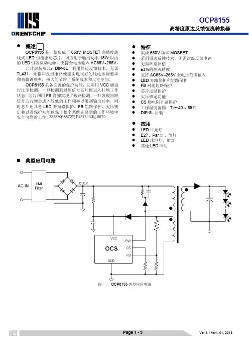
TA8155FN中文资料
- 格式:pdf
- 大小:662.32 KB
- 文档页数:16


线性CCDTSL140CL中文资料本文档由手创科技团队整理翻译,由于时间仓促与水平有限,翻译难免有所纰漏,敬请谅解并指出,谢谢。
本翻译仅为广大智能车友提供交流和参考作用!望各车友在理论中实践,在实践中创新。
各车友如有自己的心得体会,可开源共享。
最后祝愿所有参加第八届飞思卡尔智能车竞赛的同学都能有超越名次、奖金、证书以外的收获!第八届光电组交流群:185480308 181733362手创科技团队线性CCD TSL1401CL●128×1个传感器单元组织●每英寸400点(DPI)传感器间距●高线性度和均匀度●宽动态范围:4000:1(72分贝)●输出参考地●低图像延迟:0.5%典型值●操作为8 MHz。
●单3-V到5-V供应●轨到轨输出摆幅(AO)●没有外部负载电阻●更换TSL1401R-LF●符合RoHS描述TSL1401CL线性传感器阵列由一个128×1的光电二极管阵列,相关的电荷放大器电路和一个内部的像素数据保持功能组成,它提供了同时集成起始和停止时间的所有像素。
该阵列128个像素,其中每一个具有光敏面积3,524.3平方微米。
像素之间的间隔是8微米。
操作简化内部控制逻辑,只需要一个串行输入端(SI)的信号和时钟CLK。
功能框图引脚功能名称 序号 描述AO 3 模拟输出CLK 2 时钟。
时钟控制的电荷转移,像素输出和复位。
GND 6、7 接地(基板)。
所有电压都参考到基板上。
NC 5、8 无内部连接。
SI 1 串行输入。
SI定义数据输出序列的开始。
VDD 4 电源电压。
模拟和数字电路的电源电压。
详细描述该传感器是包含128个光电二极管的线性阵列。
在光电二极管的光能量冲击下产生的光电流,这是由有源积分电路,与该象素相关的集成。
在积分周期期间,采样电容器连接到积分器的输出通过一个模拟切换。
在每个像素中累积的电荷量是和光强度和积分时间成正比的。
积分器的输出和复位控制由一个128位的移位寄存器和复位逻辑控制的。
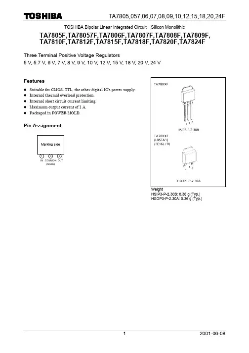
TOSHIBA Bipolar Linear Integrated Circuit Silicon MonolithicTA7805F,TA78057F,TA7806F,TA7807F,TA7808F,TA7809F, TA7810F,TA7812F,TA7815F,TA7818F,TA7820F,TA7824FThree Terminal Positive Voltage Regulators5 V, 5.7 V,6 V,7 V,8 V,9 V, 10 V, 12 V, 15 V, 18 V, 20 V, 24 VFeaturesl Suitable for CMOS, TTL, the other digital IC's power supply. l Internal thermal overload protection. lInternal short circuit current limiting. l Maximum output current of 1 A. l Packaged in POWER MOLD.Pin AssignmentIN 13OUTCOMMON (CASE)Marking side2WeightHSIP3-P-2.30B: 0.36 g (Typ.) HSOP3-P-2.30A: 0.36 g (Typ.)Equivalent CircuitMaximum Ratings (Ta = 25°C)Characteristics Symbol Rating UnitTA7805F TA78057F TA7806F TA7807F TA7808FTA7809F TA7810F TA7812F TA7815F 35TA7818F TA7820F Input voltageTA7824FV IN40V(Ta = 25°C) 1 Power dissipation (Tc = 25°C)P D 10WOperating temperature T opr −30~85 °C Storage temperature T stg −55~150 °C Junction temperature T j150 °CR th (j-c) 12.5Thermal resistanceR th (j-a) 125°C/W(Unless otherwise specified, V IN = 10 V, I OUT = 500 mA, 0°C ≤ T j ≤ 125°C)Characteristics SymbolTestCircuitTest ConditionMin Typ. Max Unit Output voltage V OUT 1 T j = 25°C, I OUT = 100 mA 4.85.05.2V7.0 V ≤ V IN ≤ 25 V ― 3 100Line regulationReg·line1T j = 25°C8.0 V ≤ V IN ≤ 12 V ― 1 50 mV 5 mA ≤ I OUT ≤ 1.4 A ― 15 100Load regulation Reg·load 1T j = 25°C250 mA ≤ I OUT ≤ 750 mA ― 5 50mV Output voltage V OUT 1 T j = 25°C7.0 V ≤ V IN ≤ 20 V 5.0 mA ≤ I OUT ≤ 1.0 A4.75― 5.25VQuiescent current I B 1 T j = 25°C, I OUT = 5 mA ― 4.2 8.0 mA Quiescent current change ∆I B 1 7.0 V ≤ V IN ≤ 25 V, I OUT = 5 mA, T j = 25°C ―― 1.3 mAOutput noise voltage V NO 2 Ta = 25°C, 10 Hz ≤ f ≤ 100 kHz I OUT = 50 mA― 50 ― µV rms Ripple rejection R.R. 3f = 120 Hz, 10 V ≤ V IN ≤ 18 V I OUT = 50 mA, T j = 25°C57 73 ― dB Dropout voltage V D 1 I OUT = 1.0 A, T j = 25°C ― 2.0 ― V Short circuit current limit I SC 1 T j = 25°C ― 1.6 ― A Average temperaturecoefficient of output voltageT CVO1 I OUT = 5 mA―−0.6― mV/°CTA78057FElectrical Characteristics(Unless otherwise specified, V IN = 10.7 V, I OUT = 500 mA, 0°C ≤ T j ≤ 125°C)Characteristics SymbolTestCircuitTest ConditionMin Typ. Max Unit Output voltage V OUT 1 T j = 25°C, I OUT = 100 mA 5.475.75.93V7.7 V ≤ V IN ≤ 25 V ― 4 110Line regulationReg·line1T j = 25°C8.7 V ≤ V IN ≤ 12.7 V ― 2 55 mV 5 mA ≤ I OUT ≤ 1.4 A ― 15 110Load regulation Reg·load 1T j = 25°C250 mA ≤ I OUT ≤ 750 mA ― 5 55mV Output voltage V OUT 1 T j = 25°C7.7 V ≤ V IN ≤ 20.7 V 5.0 mA ≤ I OUT ≤ 1.0 A5.42― 5.98VQuiescent current I B 1 T j = 25°C, I OUT = 5 mA ― 4.3 8.0 mA Quiescent current change ∆I B 1 7.7 V ≤ V IN ≤ 25 V, I OUT = 5 mA, T j = 25°C ―― 1.3 mAOutput noise voltage V NO 2 Ta = 25°C, 10 Hz ≤ f ≤ 100 kHz I OUT = 50 mA― 55 ― µV rms Ripple rejection R.R. 3f = 120 Hz, 8.8 V ≤ V IN ≤ 18.8 V, I OUT = 50 mA, T j = 25°C56 72 ― dB Dropout voltage V D 1 I OUT = 1.0 A, T j = 25°C ― 2.0 ― V Short circuit current limit I SC 1 T j = 25°C ― 1.5 ― A Average temperaturecoefficient of output voltageT CVO1 I OUT = 5 mA―−0.7― mV/°C(Unless otherwise specified, V IN = 11 V, I OUT = 500 mA, 0°C ≤ T j ≤ 125°C)Characteristics SymbolTestCircuitTest ConditionMin Typ. Max Unit Output voltage V OUT 1 T j = 25°C, I OUT = 100 mA 5.756.06.25V8.0 V ≤ V IN ≤ 25 V ― 4 120Line regulationReg·line1T j = 25°C9 V ≤ V IN ≤ 13 V ― 2 60 mV5 mA ≤ I OUT ≤ 1.4 A ― 15 120Load regulation Reg·load 1T j = 25°C250 mA ≤ I OUT ≤ 750 mA ― 5 60mV Output voltage V OUT 1 T j = 25°C8 V ≤ V IN ≤ 21 V5.0 mA ≤ I OUT ≤ 1.0 A5.7― 6.3 VQuiescent current I B 1 T j = 25°C, I OUT = 5 mA ― 4.3 8.0 mA Quiescent current change ∆I B 1 8.0 V ≤ V IN ≤ 25 V, I OUT = 5 mA, T j = 25°C ―― 1.3 mAOutput noise voltage V NO 2 Ta = 25°C, 10 Hz ≤ f ≤ 100 kHz I OUT = 50 mA― 55 ― µV rms Ripple rejection R.R. 3f = 120 Hz, 11 V ≤ V IN ≤ 19 V I OUT = 50 mA, T j = 25°C56 72 ― dB Dropout voltage V D 1 I OUT = 1.0 A, T j = 25°C ― 2.0 ― V Short circuit current limit I SC 1 T j = 25°C ― 1.5 ― A Average temperaturecoefficient of output voltageT CVO1 I OUT = 5 mA―−0.7― mV/°CTA7807FElectrical Characteristics(Unless otherwise specified, V IN = 12 V, I OUT = 500 mA, 0°C ≤ T j ≤ 125°C)Characteristics SymbolTestCircuitTest ConditionMin Typ. Max Unit Output voltage V OUT 1 T j = 25°C, I OUT = 100 mA 6.727.07.28V9 V ≤ V IN ≤ 25 V ― 5 140Line regulationReg·line1T j = 25°C10 V ≤ V IN ≤ 14 V ― 2 70mV 5 mA ≤ I OUT ≤ 1.4 A ― 15 140Load regulation Reg·load 1T j = 25°C250 mA ≤ I OUT ≤ 750 mA ― 5 70mV Output voltage V OUT 1 T j = 25°C9 V ≤ V IN ≤ 22 V5.0 mA ≤ I OUT ≤ 1.0 A6.65― 7.35VQuiescent current I B 1 T j = 25°C, I OUT = 5 mA ― 4.3 8.0 mA Quiescent current change ∆I B 1 9 V ≤ V IN ≤ 25 V,I OUT = 5 mA, T j = 25°C ―― 1.3 mAOutput noise voltage V NO 2 Ta = 25°C, 10 Hz ≤ f ≤ 100 kHz I OUT = 50 mA― 60 ― µV rms Ripple rejection R.R. 3f = 120 Hz, 12 V ≤ V IN ≤ 20 V I OUT = 50 mA, T j = 25°C54 70 ― dB Dropout voltage V D 1 I OUT = 1.0 A, T j = 25°C ― 2.0 ― V Short circuit current limit I SC 1 T j = 25°C ― 1.3 ― A Average temperaturecoefficient of output voltageT CVO1 I OUT = 5 mA―−0.8― mV/°C(Unless otherwise specified, V IN = 14 V, I OUT = 500 mA, 0°C ≤ T j ≤ 125°C)Characteristics SymbolTestCircuitTest ConditionMin Typ. Max Unit Output voltage V OUT 1 T j = 25°C, I OUT = 100 mA 7.78.08.3V10.5 V ≤ V IN ≤ 25 V ― 6 160Line regulationReg·line1T j = 25°C11 V ≤ V IN ≤ 17 V ― 2 80mV 5 mA ≤ I OUT ≤ 1.4 A ― 12 160Load regulation Reg·load 1T j = 25°C250 mA ≤ I OUT ≤ 750 mA ― 4 80mV Output voltage V OUT 1 T j = 25°C10.5 V ≤ V IN ≤ 23 V 5.0 mA ≤ I OUT ≤ 1.0 A7.6― 8.4 VQuiescent current I B 1 T j = 25°C, I OUT = 5 mA ― 4.3 8.0 mA Quiescent current change ∆I B 1 10.5 V ≤ V IN ≤ 25 V, I OUT = 5 mA, T j = 25°C ―― 1.0 mAOutput noise voltage V NO 2 Ta = 25°C, 10 Hz ≤ f ≤ 100 kHz I OUT = 50 mA― 70 ― µV rms Ripple rejection R.R. 3f = 120 Hz, 14 V ≤ V IN ≤ 21.5 V I OUT = 50 mA, T j = 25°C53 69 ― dB Dropout voltage V D 1 I OUT = 1.0 A, T j = 25°C ― 2.0 ― V Short circuit current limit I SC 1 T j = 25°C ― 1.1 ― A Average temperaturecoefficient of output voltageT CVO1 I OUT = 5 mA―−1.0― mV/°CTA7809FElectrical Characteristics(Unless otherwise specified, V IN = 15 V, I OUT = 500 mA, 0°C ≤ T j ≤ 125°C)Characteristics SymbolTestCircuitTest ConditionMin Typ. Max Unit Output voltage V OUT 1 T j = 25°C, I OUT = 100 mA 8.649.09.36V11.5 V ≤ V IN ≤ 26 V ― 7.0 180Line regulationReg·line1T j = 25°C13 V ≤ V IN ≤ 19 V ― 2.5 90mV 5 mA ≤ I OUT ≤ 1.4 A ― 12 180Load regulation Reg·load 1T j = 25°C250 mA ≤ I OUT ≤ 750 mA ― 4 90mV Output voltage V OUT 1 T j = 25°C11.5 V ≤ V IN ≤ 24 V 5.0 mA ≤ I OUT ≤ 1.0 A8.55― 9.45VQuiescent current I B 1 T j = 25°C, I OUT = 5 mA ― 4.3 8.0 mA Quiescent current change ∆I B 1 11.5 V ≤ V IN ≤ 26 V, I OUT = 5 mA, T j = 25°C ―― 1.0 mAOutput noise voltage V NO 2 Ta = 25°C, 10 Hz ≤ f ≤ 100 kHz I OUT = 50 mA― 75 ― µV rms Ripple rejection R.R. 3f = 120 Hz, 15 V ≤ V IN ≤ 22.5 V I OUT = 50 mA, T j = 25°C51 67 ― dB Dropout voltage V D 1 I OUT = 1.0 A, T j = 25°C ― 2.0 ― V Short circuit current limit I SC 1 T j = 25°C ― 1.0 ― A Average temperaturecoefficient of output voltageT CVO1 I OUT = 5 mA―−1.1― mV/°C(Unless otherwise specified, V IN = 16 V, I OUT = 500 mA, 0°C ≤ T j ≤ 125°C)Characteristics SymbolTestCircuitTest ConditionMin Typ. Max Unit Output voltage V OUT 1 T j = 25°C, I OUT = 100 mA 9.610.010.4V 12.5 V ≤ V IN ≤ 27 V ― 8 200Line regulationReg·line1T j = 25°C14 V ≤ V IN ≤ 20 V ― 2.5 100mV5 mA ≤ I OUT ≤ 1.4 A ― 12 200Load regulation Reg·load 1T j = 25°C250 mA ≤ I OUT ≤ 750 mA ― 4 100mV Output voltage V OUT 1 T j = 25°C12.5 V ≤ V IN ≤ 25 V 5.0 mA ≤ I OUT ≤ 1.0 A9.5― 10.5VQuiescent current I B 1 T j = 25°C, I OUT = 5 mA ― 4.3 8.0 mA Quiescent current change ∆I B 1 12.5 V ≤ V IN ≤ 27 V, I OUT = 5 mA, T j = 25°C ―― 1.0 mAOutput noise voltage V NO 2 Ta = 25°C, 10 Hz ≤ f ≤ 100 kHz I OUT = 50 mA― 80 ― µV rms Ripple rejection R.R. 3f = 120 Hz, 16 V ≤ V IN ≤ 23.5 V I OUT = 50 mA, T j = 25°C50 66 ― dB Dropout voltage V D 1 I OUT = 1.0 A, T j = 25°C ― 2.0 ― V Short circuit current limit I SC 1 T j = 25°C ― 0.9 ― A Average temperaturecoefficient of output voltageT CVO1 I OUT = 5 mA―−1.3― mV/°CTA7812FElectrical Characteristics(Unless otherwise specified, V IN = 19 V, I OUT = 500 mA, 0°C ≤ T j ≤ 125°C)Characteristics SymbolTestCircuitTest ConditionMin Typ. Max Unit Output voltage V OUT 1 T j = 25°C, I OUT = 100 mA 11.512.012.5V 14.5 V ≤ V IN ≤ 30 V ― 10 240Line regulationReg·line1T j = 25°C16 V ≤ V IN ≤ 22 V ― 3 120mV5 mA ≤ I OUT ≤ 1.4 A ― 12 240Load regulation Reg·load 1T j = 25°C250 mA ≤ I OUT ≤ 750 mA ― 4 120mV Output voltage V OUT 1 T j = 25°C14.5 V ≤ V IN ≤ 27 V 5.0 mA ≤ I OUT ≤ 1.0 A11.4― 12.6VQuiescent current I B 1 T j = 25°C, I OUT = 5 mA ― 4.3 8.0 mA Quiescent current change ∆I B 1 14.5 V ≤ V IN ≤ 30 V, I OUT = 5 mA, T j = 25°C ―― 1.0 mAOutput noise voltage V NO 2 Ta = 25°C, 10 Hz ≤ f ≤ 100 kHz I OUT = 50 mA― 90 ― µV rms Ripple rejection R.R. 3f = 120 Hz, 19 V ≤ V IN ≤ 25 V I OUT = 50 mA, T j = 25°C50 66 ― dB Dropout voltage V D 1 I OUT = 1.0 A, T j = 25°C ― 2.0 ― V Short circuit current limit I SC 1 T j = 25°C ― 0.7 ― A Average temperaturecoefficient of output voltageT CVO1 I OUT = 5 mA―−1.6― mV/°C(Unless otherwise specified, V IN = 23 V, I OUT = 500 mA, 0°C ≤ T j ≤ 125°C)Characteristics SymbolTestCircuitTest ConditionMin Typ. Max Unit Output voltage V OUT 1 T j = 25°C, I OUT = 100 mA 14.415.015.6V 17.5 V ≤ V IN ≤ 30 V ― 11 300Line regulationReg·line1T j = 25°C20 V ≤ V IN ≤ 26 V ― 3 150mV5 mA ≤ I OUT ≤ 1.4 A ― 12 300Load regulation Reg·load 1T j = 25°C250 mA ≤ I OUT ≤ 750 mA ― 4 150mV Output voltage V OUT 1 T j = 25°C17.5 V ≤ V IN ≤ 30 V 5.0 mA ≤ I OUT ≤ 1.0 A14.25― 15.75VQuiescent current I B 1 T j = 25°C, I OUT = 5 mA ― 4.4 8.0 mA Quiescent current change ∆I B 1 17.5 V ≤ V IN ≤ 30 V, I OUT = 5 mA, T j = 25°C ―― 1.0 mAOutput noise voltage V NO 2 Ta = 25°C, 10 Hz ≤ f ≤ 100 kHz I OUT = 50 mA― 110 ― µV rms Ripple rejection R.R. 3f = 120 Hz, 23 V ≤ V IN ≤ 28.5 V I OUT = 50 mA, T j = 25°C49 65 ― dB Dropout voltage V D 1 I OUT = 1.0 A, T j = 25°C ― 2.0 ― V Short circuit current limit I SC 1 T j = 25°C ― 0.5 ― A Average temperaturecoefficient of output voltageT CVO1 I OUT = 5 mA―−2.0― mV/°CTA7818FElectrical Characteristics(Unless otherwise specified, V IN = 27 V, I OUT = 500 mA, 0°C ≤ T j ≤ 125°C)Characteristics SymbolTestCircuitTest ConditionMin Typ. Max Unit Output voltage V OUT 1 T j = 25°C, I OUT = 100 mA 17.318.018.7V 21 V ≤ V IN ≤ 33 V ― 13 360Line regulationReg·line1T j = 25°C24 V ≤ V IN ≤ 30 V ― 4 180mV5 mA ≤ I OUT ≤ 1.4 A ― 12 360Load regulation Reg·load 1T j = 25°C250 mA ≤ I OUT ≤ 750 mA ― 4 180mV Output voltage V OUT 1 T j = 25°C21 V ≤ V IN ≤ 33 V 5.0 mA ≤ I OUT ≤ 1.0 A17.1― 18.9VQuiescent current I B 1 T j = 25°C, I OUT = 5 mA ― 4.5 8.0 mA Quiescent current change ∆I B 1 21 V ≤ V IN ≤ 33 V,I OUT = 5 mA, T j = 25°C ―― 1.0 mAOutput noise voltage V NO 2 Ta = 25°C, 10 Hz ≤ f ≤ 100 kHz I OUT = 50 mA― 125 ― µV rms Ripple rejection R.R. 3f = 120 Hz, 27 V ≤ V IN ≤ 32 V I OUT = 50 mA, T j = 25°C47 63 ― dB Dropout voltage V D 1 I OUT = 1.0 A, T j = 25°C ― 2.0 ― V Short circuit current limit I SC 1 T j = 25°C ― 0.4 ― A Average temperaturecoefficient of output voltageT CVO1 I OUT = 5 mA―−2.5― mV/°C(Unless otherwise specified, V IN = 29 V, I OUT = 500 mA, 0°C ≤ T j ≤ 125°C)Characteristics SymbolTestCircuitTest ConditionMin Typ. Max Unit Output voltage V OUT 1 T j = 25°C, I OUT = 100 mA 19.220.020.8V 23 V ≤ V IN ≤ 35 V ― 15 400Line regulationReg·line1T j = 25°C26 V ≤ V IN ≤ 32 V ― 5 200mV5 mA ≤ I OUT ≤ 1.4 A ― 12 400Load regulation Reg·load 1T j = 25°C250 mA ≤ I OUT ≤ 750 mA ― 4 200mV Output voltage V OUT 1 T j = 25°C23 V ≤ V IN ≤ 35 V 5.0 mA ≤ I OUT ≤ 1.0 A19.0― 21.0VQuiescent current I B 1 T j = 25°C, I OUT = 5 mA ― 4.6 8.0 mA Quiescent current change ∆I B 1 23 V ≤ V IN ≤ 35 V,I OUT = 5 mA, T j = 25°C ―― 1.0 mAOutput noise voltage V NO 2 Ta = 25°C, 10 Hz ≤ f ≤ 100 kHz I OUT = 50 mA― 135 ― µV rms Ripple rejection R.R. 3f = 120 Hz, 29 V ≤ V IN ≤ 34 V I OUT = 50 mA, T j = 25°C45 61 ― dB Dropout voltage V D 1 I OUT = 1.0 A, T j = 25°C ― 2.0 ― V Short circuit current limit I SC 1 T j = 25°C ― 0.4 ― A Average temperaturecoefficient of output voltageT CVO1 I OUT = 5 mA―−3.0― mV/°CTA7824FElectrical Characteristics(Unless otherwise specified, V IN = 33 V, I OUT = 500 mA, 0°C ≤ T j ≤ 125°C)Characteristics SymbolTestCircuitTest ConditionMin Typ. Max Unit Output voltage V OUT 1 T j = 25°C, I OUT = 100 mA 23.024.025.0V 27 V ≤ V IN ≤ 38 V ― 18 480Line regulationReg·line1T j = 25°C30 V ≤ V IN ≤ 36 V ― 6 240mV5 mA ≤ I OUT ≤ 1.4 A ― 12 480Load regulation Reg·load 1T j = 25°C250 mA ≤ I OUT ≤ 750 mA ― 4 240mV Output voltage V OUT 1 T j = 25°C27 V ≤ V IN ≤ 38 V 5.0 mA ≤ I OUT ≤ 1.0 A22.8― 25.2VQuiescent current I B 1 T j = 25°C, I OUT = 5 mA ― 4.6 8.0 mA Quiescent current change ∆I B 1 27 V ≤ V IN ≤ 38 V,I OUT = 5 mA, T j = 25°C ―― 1.0 mAOutput noise voltage V NO 2 Ta = 25°C, 10 Hz ≤ f ≤ 100 kHz I OUT = 50 mA― 150 ― µV rms Ripple rejection R.R. 3f = 120 Hz, 33 V ≤ V IN ≤ 38 V I OUT = 50 mA, T j = 25°C45 61 ― dB Dropout voltage V D 1 I OUT = 1.0 A, T j = 25°C ― 2.0 ― V Short circuit current limit I SC 1 T j = 25°C ― 0.3 ― A Average temperaturecoefficient of output voltageT CVO1 I OUT = 5 mA―−3.5― mV/°CTest Circuit 1/Standard Application CircuitTest Circuit 2V NOTest Circuit 3R.R.Precautions on Application(1) In regard to GND, be careful not to apply a negative voltage to the input/output terminal. Further,special care is necessary in case of a voltage boost application.(2) When a surge voltage exceeding maximum rating is applied to the input terminal or when a voltagein excess of the input terminal voltage is applied to the output terminal, the circuit may be destroyed.Specially, in the latter case, great care is necessary.Further, if the input terminal shorts to GND in a state of normal operation, the output terminalvoltage becomes higher than the input voltage (GND potential), and the electric charge of a chemicalcapacitor connected to the output terminal flows into the input side, which may cause the destructionof circuit.In these cases, take such steps as a zener diode and a general silicon diode are connected to the circuit,as shown in the following figure.(3) When the input voltage is too high, the power dissipation of three terminal regulator increasesbecause of series regulator, so that the junction temperature rises. In such a case, it is recommendedto reduce the power dissipation by inserting the power limiting resistor R SD in the input terminal,and to reduce the junction temperature as a result.The power dissipation P D of IC is expressed in the following equation.V IN' is reduced below the lowest voltage necessary for the IC, the parasitic oscillation will be caused Ifaccording to circumstances.In determing the resistance value of R SD, design with margin should be made by making reference tothe following equation.(4) Connect the input terminal and GND, and the output terminal and GND, by capacitor respectively.The capacitances should be determined experimentally because they depend on PCB patterns. Inparticular, adequate investigation should be made so that there is no problem even at time of high orlow temperature.(5)The molded plastic portion of this unit, measuring 5.5 mm (L) by 6.8 mm (W) by 2.5 mm (T), is more comapact compared to its equivalents TO-220.The GND fin extends directly out of the main body, and can be soldered directly to the ceramic circuit board, to significantly increase the power dissipation.For obtaining high reliability on the heat sink design of the regulator IC, it is generally required to derate more than 20% of maximum junction temperature (T j max). Further, full consideration should be given to the installation of IC to the heat sink.Application Circuits(1)Voltage boost regulator(a)Voltage boost by use of zener diode(b) Voltage boost by use of resistor(c) Adjustable output regulatorregulatorboost(2) Current· TOSHIBA is continually working to improve the quality and reliability of its products. Nevertheless, semiconductor devices in general can malfunction or fail due to their inherent electrical sensitivity and vulnerability to physical stress. It is the responsibility of the buyer, when utilizing TOSHIBA products, to comply with the standards of safety in making a safe design for the entire system, and to avoid situations in which a malfunction or failure of such TOSHIBA products could cause loss of human life, bodily injury or damage to property.In developing your designs, please ensure that TOSHIBA products are used within specified operating ranges as set forth in the most recent TOSHIBA products specifications. Also, please keep in mind the precautions and conditions set forth in the “Handling Guide for Semiconductor Devices,” or “TOSHIBA Semiconductor Reliability Handbook” etc.. · The TOSHIBA products listed in this document are intended for usage in general electronics applications (computer, personal equipment, office equipment, measuring equipment, industrial robotics, domestic appliances, etc.). These TOSHIBA products are neither intended nor warranted for usage in equipment that requires extraordinarily high quality and/or reliability or a malfunction or failure of which may cause loss of human life or bodily injury (“Unintended Usage”). Unintended Usage include atomic energy control instruments, airplane or spaceship instruments, transportation instruments, traffic signal instruments, combustion control instruments, medical instruments, all types of safety devices, etc.. Unintended Usage of TOSHIBA products listed in this document shall be made at the customer’s own risk. · The products described in this document are subject to the foreign exchange and foreign trade laws.· The information contained herein is presented only as a guide for the applications of our products. No responsibility is assumed by TOSHIBA CORPORATION for any infringements of intellectual property or other rights of the third parties which may result from its use. No license is granted by implication or otherwise under any intellectual property or other rights of TOSHIBA CORPORATION or others. · The information contained herein is subject to change without notice.000707EBARESTRICTIONS ON PRODUCT USE。