AD将PCB导出成IDF并导入FLOEDA教程
- 格式:pdf
- 大小:257.69 KB
- 文档页数:2
ad原理图导入pcb在PCB设计中,AD原理图的导入是一个非常重要的步骤。
AD原理图是指Analog Devices公司生产的一款电路设计软件,它可以帮助工程师完成电路设计、仿真和验证等工作。
而将AD原理图导入到PCB中,则是将电路设计转化为实际的电路板布局和布线,是整个电路设计流程中的关键一环。
首先,我们需要明确AD原理图导入到PCB中的目的。
将AD原理图导入到PCB中,可以直接将电路设计转化为PCB布局图,省去了手动布局和布线的繁琐过程,提高了设计效率。
同时,由于AD原理图和PCB设计软件之间可以进行数据交换,因此导入后可以直接进行电路仿真和验证,确保设计的准确性和稳定性。
在进行AD原理图导入到PCB之前,我们需要做一些准备工作。
首先,需要确保AD原理图中的元件和连线都是准确无误的,因为这些数据将直接影响到后续的PCB布局和布线。
其次,需要选择合适的PCB设计软件,确保它能够兼容AD原理图的数据格式,并且支持数据的导入和转换。
最后,需要对PCB的布局和布线规则进行一定的设置,以满足实际的电路板制造和组装要求。
在进行AD原理图导入到PCB的过程中,需要注意一些关键步骤。
首先,需要将AD原理图的数据导出为标准的数据格式,通常是通过导出为EDIF、DXF等格式的文件。
然后,将导出的文件导入到PCB设计软件中,进行数据的解析和转换。
在这一过程中,需要确保元件的对应关系和连线的连接正确无误,避免数据丢失或错误。
最后,需要进行布局和布线的优化,以满足电路板的性能、尺寸和制造要求。
在完成AD原理图导入到PCB的过程后,需要进行一定的验证和调整。
首先,需要进行电路的仿真和验证,确保电路的性能和稳定性符合设计要求。
其次,需要对PCB的布局和布线进行优化和调整,以满足实际的电路板制造和组装要求。
最后,需要进行一定的审查和确认,确保整个设计流程的准确性和可靠性。
总的来说,AD原理图导入到PCB是一个重要而复杂的过程,需要我们在设计和操作上非常谨慎和细致。
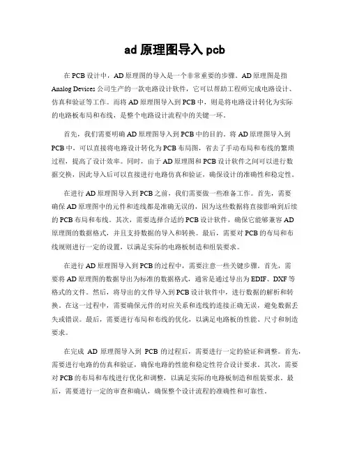
Allegro如何输出IDF文件操作指导Allegro支持输出IDF文件,用于导入结构软件中检查和查看,具体操作如下1.点击File-export-IDF2.会弹出一个对话框,file name type选择IDF3.然后点击export,输出IDF文件,文件已经输出This section is describe what the function allegro have ,helpfully could let user know more about allegroAllegro Design and Analysis includes design authoringPCB layout and Library and Design Data ManagementWith. It can ensure the end-to-end design of PCB with high quality andefficiencyRealize smooth data transfer between tools, shorten PCB design cycle, and shorten productMarket time1. Design authoringProvide a flexible logic constraint driven flow, management design rules, network hierarchy,Bus and differential pair.1.1.1 Main features and functionsThrough hierarchical and design "derivation" function, improve the original of complex designMap editing efficiency.Powerful CIS helps users quickly determine part selection and accelerate design flowAnd reduce project cost.1.2.1 Main featuresSchematic designers and PCB design engineers can work in parallel. Advanced design efficiency improves functions, such as copying the previous schematic design Select multiplexing with or by page. Seamless integration into pre simulation and signal analysis.1.2.2 Main FunctionsProvide schematic diagram and HDL/Verilog design input.Assign and manage high-speed design rules.Support netclasses, buses, extension networks and differential pairs. Powerful library creation and management functions.Allows synchronization of logical and physical designs.Realize multi-user parallel development and version control.Pre integration simulation and signal analysis.Support customizable user interface and enterprise customization development.1.3 o Allegro n Design Publisher1.3.1 Main Features and FunctionsAllows you to share designs with others using PDF files.The entire design is represented in a single, compact PDF format. Improve design readability.Provide content control - users can select the content to be published.1.4 Allegro A FPGA m System Planner1 1.4.1 Main features and functionsComplete and scalable FPGA/PCB collaborative design technology for ideal "Design and correct "pin assignment.Scalable FPGA/PCB protocol from OrCAD Capture to Allegro GXLSame as the design solution.Shorten the optimization pin allocation time and accelerate the PCBdesign cycle.2. B PCB layoutIt provides expandable and easy to use PCB design (including RFPCB) Then drive PCB design solution. It also includes innovative new automatic deliveryMutual technology can effectively improve the wiring of high-speed interfaces; Apply EDMD (IDX) mode, which makes ECAD/MCAD work smoothly; Execute modern industry standard IPC-2581,Ensure that the design data is simply and high-quality transferred to the downstream link.2.1.1 Main featuresSpeed up the design process from layout, wiring to manufacturing. Including powerful functions, such as design zoning, RF design functions and global design rules Stroke.It can improve productivity and help engineers to quickly move up to mass production* g- M4 G8 |6 }9 k7 G2.1.2 Main FunctionsProvide scalable full function PCB design solutions.Enable constraint driven design processes to reduce design iterations. Integrated DesignTrueDFM technology provides real-time DFM inspection. Provide a single, consistent context for management.Minimize design iterations and reduce overall Flex and rigid flexible designCost, and has advanced rigid and flexible design functions.Realize dynamic concurrent team design capability, shorten design cycle, and greatly reduceTime spent in routing, winding and optimization.Provide integrated RF/analog design and mixed signal design environment. Provides interactive layout and component placement.Provide design partitions for large distributed development teams. Realize real-time, interactive push editing of routing.It is allowed to use dynamic copper sheet technology to edit and update in real time.Manage netscheduling, timing, crosstalk, routing by designated layer and area Bundle.Provide proven PCB routing technology for automatic routing.Realize hierarchical route planning and accelerate the completion of design.Shorten interconnect planning and cabling time for high-speed interface intensive design.Provide a comprehensive, powerful and easy-to-use tool suite to help designersEfficient and successful manufacturing switch: DFM Checker is aimed at the company/manufacturerReview the specific rules of manufacturing partners; Used to reduce manufacturing and assembly documentsThe document editing time of the file can reach 70%; The panel editor will assemble the panel designThe intention is communicated to the manufacturing partners; Output design data in various manufacturing formats.3. y Library d and n Design a Data ManagementFor cost-effective projects that need to be delivered on time, it is easy to obtainCurrent component information and design data are critical. library and designData management is a collaborative control of the company's internal cooperation and design processAdvanced functions are provided. As the design cycle shortens and the complexity increases, youThere must be a design approach that increases predictability and accelerates design turnaround.3.1.1 Main featuresReduce time and optimize library development related resources. Improve the precision in the process of parts manufacturing. Q9 b3.1.2 Main functionsReduce time and optimize library development and validation through integrated creation and validation processes Certification related resources.A simple method to develop devices with large pin count can shorten the time from a few days to A few minutes.Powerful graphic editor supports custom shape and spreadsheet import forSchematic symbols are created to ensure the reliability and integrity of data.Supports the import of part information from general industry formats, allowing rapid creation and Update part information.Common library development environment supporting schematic tools from different suppliers, including Mentor Graphics Design Architect and Mentor Graphics Viewdraw。
Prel和Alium Designer免费专题培训之:AD导入导出-V1AD(Alium Designer)是一款广泛应用于电路设计领域的高端EDA工具,而Prel则是一种基于脚本的EDA软件。
本文将带领大家了解如何导入和导出AD中的设计数据。
一、AD导入导出概述在设计过程中,有时需要将AD中的设计数据导入到其他软件中进行进一步操作,此时需要注意以下几点:1. 文件格式:导出的数据格式必须是其他软件所支持的格式,如常见的EDIF、OASIS等格式。
2. 导入数据:导入数据时需要将数据正确地映射到目标软件的对应层次结构中,保证正确性和完整性。
3. 设计规则:在导入数据后,需要根据目标软件的设计规则进行验证和修复。
二、AD导入数据AD支持将设计数据导出为多种格式,并可以根据需要进行选择,这里以EDIF格式为例:1. 打开需要导出数据的工程文件,在项目管理栏中选择“输出文件”选项,点击“添加输出文件”按钮。
2. 在弹出窗口中选择“EDIF”格式,点击“确定”按钮。
3. 在弹出的窗口中选择需要导出的设计数据,包括原理图、布局等。
4. 点击“开始导出”按钮,将数据导出到指定的文件夹中。
三、AD导出数据在导出AD数据时,需要切换到目标软件的导入界面,选择正确的数据格式,将数据导入。
以下以Prel为例进行说明:1. 在Prel中打开需要导入的工程文件,在项目管理栏中选择“导入文件”选项,点击“添加导入文件”按钮。
2. 在弹出窗口中选择需要导入的文件格式为EDIF,点击“确定”按钮。
3. 在弹出的窗口中选择需要导入的数据文件,点击“开始导入”按钮。
4. 数据导入后,根据目标软件的设计规则进行验证和修复。
总结AD和Prel都是常见的EDA工具,在设计过程中需要进行数据的导入和导出操作。
本文介绍了AD中如何导出数据到其他软件,以及如何从其他软件中导入数据到AD中,并指出了需要注意的问题。
合理地进行导入导出操作,可以提高设计效率和成果的质量。
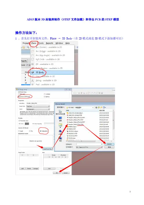
AD15版本3D封装库制作(STEP文件加载)和导出PCB的STEP模型操作方法如下:1 、首先打开封装库文件,Place → 3D Body(在2D模式或是3D模式下添加都可以)2 、参数设置放置好后,弹出对话框,点击取消,接下来就是准确放置3D模型和封装匹配对于贴片的3D模型,放置个大概位置就好(3D模型放置在封装上面,高度适合就行)。
对于插件的3D模型,要准确放置,有个很好的技巧,软件可以在3D模型上添加捕捉点,Tools → 3D Body Placement → Add Snap Points From Vertices单击要添加捕捉点的引脚,移动鼠标出现蓝色十字光标,把十字光标移至引脚的一个棱角处,如下图,此时按一下 空格键,(鼠标不要移动)再单击一下左键,然后把光标(鼠标)移至对角的棱角处,此时单击左键,出现白色的十字架,说明捕捉引脚中心已经成功,点击右键,结束捕捉。
切换回2D模式下把白色的十字光标移至焊盘的中心,软件会自动捕捉的,如上面右侧的图如果不想要白色的大十字光标,可以在3D模式下删除捕捉点,Tools → 3D Body Placement → Remove Snap Points看下3D效果,发现有部分 实体在丝印层的下方,需要调整一下高度,可以双击3D模型,弹出来的对话框中Standoff Height修改参数,调至到合适的高度。
这里有个快速匹配高度的方法,Tools → 3D Body Placement →Set Body Height,点击一下3D模型。
出现蓝色十字光标,把蓝色十字光标移至黑色实体底部捕捉一个棱角,如下图此时单击左键, 弹出对话框,如上面右侧图,点击OK。
调整后效果如下图保存封装库。
接下来就是如何把3D封装更新到PCB里3 、更新封装 把3D封装更新到PCB里,实现PCB中显示3D模型最好把封装库和已经画好的PCB文件放在同一个工程目录下,并且PCB文件已经打开(如果工程里没有建立PCB文件,通过原理图调用封装就可以把3D模型更新到将要建立的PCB文件中)4 、导出PCB 的Step 模型File → Export → STEP 3D (AD15版本导出方法) 命名保存,在弹出来的对话框设置导出的内容。
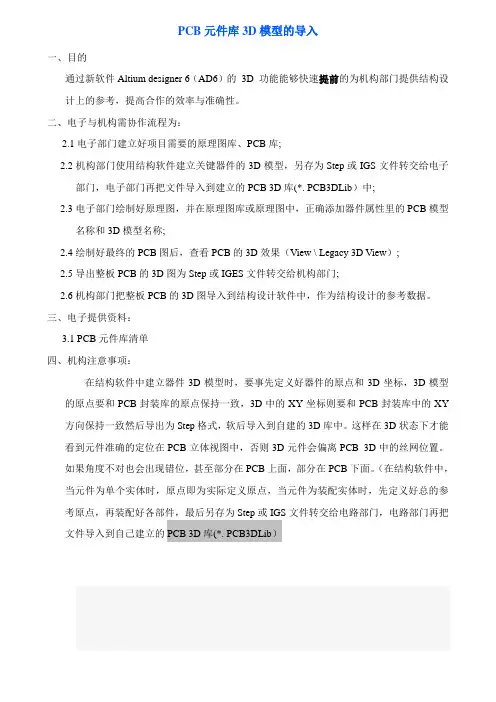
PCB元件库3D模型的导入一、目的通过新软件Altium designer 6(AD6)的3D 功能能够快速提前的为机构部门提供结构设计上的参考,提高合作的效率与准确性。
二、电子与机构需协作流程为:2.1电子部门建立好项目需要的原理图库、PCB库;2.2机构部门使用结构软件建立关键器件的3D模型,另存为Step或IGS文件转交给电子部门,电子部门再把文件导入到建立的PCB 3D库(*. PCB3DLib)中;2.3电子部门绘制好原理图,并在原理图库或原理图中,正确添加器件属性里的PCB模型名称和3D模型名称;2.4绘制好最终的PCB图后,查看PCB的3D效果(View \ Legacy 3D View);2.5导出整板PCB的3D图为Step或IGES文件转交给机构部门;2.6机构部门把整板PCB的3D图导入到结构设计软件中,作为结构设计的参考数据。
三、电子提供资料:3.1 PCB元件库清单四、机构注意事项:在结构软件中建立器件3D模型时,要事先定义好器件的原点和3D坐标,3D模型的原点要和PCB封装库的原点保持一致,3D中的XY坐标则要和PCB封装库中的XY 方向保持一致然后导出为Step格式,软后导入到自建的3D库中。
这样在3D状态下才能看到元件准确的定位在PCB立体视图中,否则3D元件会偏离PCB 3D中的丝网位置。
如果角度不对也会出现错位,甚至部分在PCB上面,部分在PCB下面。
(在结构软件中,当元件为单个实体时,原点即为实际定义原点,当元件为装配实体时,先定义好总的参考原点,再装配好各部件,最后另存为Step或IGS文件转交给电路部门,电路部门再把文件导入到自己建立的PCB 3D库(*. PCB3DLib)电子与机构需协作流程为:1.电子部门建立好项目需要的原理图库、PCB库.2.机构部门使用结构软件建立关键器件的3D模型,另存为Step文件转交给电子部门,电子部门再把文件导入到建立的PCB 封装库中.3.电子部门在原理图库中,正确添加器件属性里的PCB封装名称;并最终生成集成库(*.intlib).4.电子部门在设计中使用集成库(*.intlib)中的元器件.绘制好最终的PCB图后,查看PCB的3D效果(View \ switch to 3D).5.导出整板PCB的3D图为Step文件转交给机构部门.6.机构部门把整板PCB的3D图导入到结构设计软件中,作为结构设计的参考数据。
AD用户、组织单元的导入和导出AD用户的导入和导出工具有很多种,这里只解释微软官方提供的工具第三方工具,通过API、ADSI二次开发的工具不在讨论之列。
在下接触AD 不就,文中难免疏漏,还请各位指正,先行谢过。
入门演示在c:\下面保存此文件为test.csv 路径和文件名可以使用其它注意别留多余的空格自找麻烦其实也就是这样一个表用逗号分割的形式写,最后一项后面不写逗号然后再命令行下输入下面指令第一条type test.csv是为了显示文本中的内容第二条是用来导入用户的命令用户已经导入了,但用户是禁用的。
如果要该用户能登陆域要把用户启用。
DN objectClass sAMAccountName 这三个属性是必须的,也是最少的导入属性。
大批量导入用户这样导入只是为了有个初步的认识,下面介绍一些实际操作中的问题。
比如一个测试AD,为了模拟生产AD的环境,需要把用户和组织单元全部导入,事实上我遇到了一个上百个组织单元,接近7000个用户信息的导入操作,涉及真实信息需要保密,此处只还是做一个模拟的例子。
既然需要导入这么多用户,肯定要有相应的信息了,于是我得到了两个csv文件。
一个是组织单元的导出文件,一个是用户的导出文件。
文件的内容不便透露,这里还是模拟一下。
下面再test下面建几个组织单元(OU),如图。
然后建几个用户分别放进对应的ou里,格式从前向后依次是最小的ou,如下格式DN,objectClass,sAMAccountName"CN=testAA,OU=test11,OU=test1,OU=test,DC=bjtest,DC=com",user,testAA"CN=testbb,OU=test12,OU=test1,OU=test,DC=bjtest,DC=com",user,testbb"CN=testcc,OU=test2,OU=test,DC=bjtest,DC=com",user,testcc用户已经导入,注意这种最简的导入方式用户默认是禁用的,并且是没有密码的,后面将讲解怎么批量添加密码。
AD 6.0的导入导出功能Altium Designer 6.0提供了导入向导工具,可以很方便地导入以往Protel的设计文档和其他EDA设计工具的设计文档。
包括原理图设计文件、PCB设计文件、原理图库文件和PCB设计文件。
并可以把修改后的设计文件反存回需要的格式。
AD6.0 目前支持的设计文件格式如下:原理图文件Sch∙ V4 (Protel 99 SE) - This format can also be opened in all Windows versions of the schematic editor.PCB∙ V4 (Protel 99 SE)∙ V3 (Protel 98)∙ V2.8 (PCB 2.8)1. Check that the PADS PCB file has been exported in ASCII format. The PADS Importer is only capable of translating ASCII file format.2. View the PADS ASCII PCB file in Notepad or similar and check the file version and units displayedin the file header. This is typically found on the first line in the ASCII file. Compare this to theversions the PADS Importer is capable of translating.The translator imports the following PADS® PCB ASCII file formats:1. PowerPCB® V1, V1.1, V1.5, V2, V3.0, V3.52. PADS® Perform3. PADS® 2000 V3, V44. PADS® PCB V53. When you export the file from the PADS Software, ensure that you Select All sectionsto be exported instead of selecting particular primitives to export.4. Check that the exported file loads back into PADS Software correctly.5. Map the layers adequately. You will need to assign internal planes manually. Once the PCB file istranslated, associate the internal planes in the layer stack manager with the approriate net. Splitplanes will need to be replaced and setup in Protel.Altium Designer Knowledge BaseItem - 4488Logged: 22-Jul-2004 Revised: 23-Aug-2005Topic: Data Files - ExportingApplies To: Protel 2004;Nexar 2004;CircuitStudio 2004;Query: How do I Import and Export Altium Designer Schematic and Schematic Library files to and from OrCad Capture?Answer:Exporting Schematic documents to Orcad Capture:You cannot export a Schematic sheet as a single entity to Orcad Capture. You have to export the whole project from Altium Designer to Orcad Capture. You can do this by following the steps below:1. Within the Projects Panel, right click on the project and select the Save Project As...command.2. Within the Save As dialog, set the Save as type field to Export Orcad Capture Design (*.DSN) and click the Save button.Importing Orcad Capture Schematic files:File » Open and then select OrCad Capture Design (*.DSN) from the dropdown box and to1. Goclick on Open.Importing Orcad Capture libraries:Altium Designer can Import Orcad Schematic (*.OLB) and PCB (*.LLB) libraries:File » Open.to1. Go2. In the Choose Document to Open dialog under Files of type, select either OrCad CaptureLibrary (*.OLB) or OrCad Max Library file (*.LLB) respectively to open an OrCad Schematic orPCB library in Altium Designer.Query: How can I export a PCB board to HyperLynx (*.HYP) format?Answer: PCB documents can be saved in HyperLynx format using the File » Save As command and then selecting the Export HyperLynx (*.HYP) option in the Save as type drop down list of the Save As dialog.Note:The Stackup information is not exported properly for multilayer boards so this section will need to be updated manually in a text editor.1. Open the exported *.HYP file in a text editor and locate the STACKUP section at thebeginning of the file2. In the PCB editor, select the Design » Layer Stackup Manager command3. Looking at the Layer Stack Up in the Layer Stack Up Manager, edit the STACKUP in the *.HYP filefrom top to bottom using the syntax belowFor Top/Bottom Layers and MidLayers:(SIGNAL T=0.0014 P=0.0000 C=1.724e - 8 L=Top_Layer M=COPPER)T = copper thickness of the layer in InchC = resistivity of the conductor of the layer in Ohm x mL = name of the LayerM = material of the layer - COPPER for signal layersFor isolation substrate(DIELECTRIC T=0.0200 C=4.8000 L=DE_Internal_Plane_1 M=FR4)T = dielectric thickness of the layer in InchC = dielectric constantL = name of the LayerM = material of the dielectricFor Internal Planes(PLANE T=0.0014 C=1.724e - 8 L=Internal_Plane_1 M=COPPER)T = copper thickness of the layer in InchC = resistivity of the conductor of the layer in Ohm x mL = name of the LayerM = material of the layer - COPPER for internal planesQuery: How do I import P-CAD libraries into Altium Designer?Details: To bring in ASCII formatted libraries from P-CAD 2002 to Altium Designer, make sure that, in P-CAD 2002 in the Library Executive, lib files translate to the .lia file format using the Library » Translate command.To open a P-CAD Schematic library in Altium Designer, go to File » Open then set the Files of Type to PCAD V16,V17 ASCII Schematic library . Now browse to find the .lia file generated from P-CAD and click on Open. This should open the schematic library in Altium Designer.To import the PCB library into Altium Designer, go to File » New » PCB Library then Save the library by going to File » Save As.... After saving the library , go to File » Import » PCAD V16 ASCII library . From the PCAD ASCII Lib File dialog box, make sure you choose the .lia file which is the same .lia file from which you extracted the component symbols for the schematic library and click on open. This should populate the PCB Library with the footprints in the library.。
Altium Designer(AD)导出原理图本人用的AD版本是13.2。
对于一个复杂的电路原理图,如果用截图的方法来导出原理图,会使得导出的原理图放大后很不清晰,那么有什么办法来解决这个问题呢?下面有几种方法就能很好的解决这个问题。
一、直接复制原理图1、选择原理图中的部分电路或Ctrl+A选择全部原理图,但是不会选择原理图的边框和右下角的原理图信息。
然后再Ctrl+C,看图,这是选择部分电路。
2、在word中Ctrl+V。
不管你怎么放大,它都是很清晰的。
步骤1中,我用的是截图的方法,很明显可以看出有点模糊,而下图要清晰的多。
只要眼睛没有问题,都能看出来。
二、导出为PDF在AD中有一个Smart PDF功能,能直接将原理图转换为PDF文档。
此功能能将整个原理图都导出,包括边框和右下角的原理图信息。
方法如下。
· 在菜单栏中选择File –> Smart PDF,就直接点Next,接下来就是选择导出的内容和到出的PDF文档的位置,这些都是自己选择。
如果不懂的,就一直Next也没事,最后点Finish;。
完成后,会自动弹出导出的PDF文档。
·不要说我说的很简单,它本来就很简单,只是有些人找不到功能在哪里,因此变得难。
Smart PDF中的配置,相信不是傻子的人都能看懂,看不懂的也可以搜,我不说其他的了。
三、导出到word中(其实就是一种矢量图,截图的是一种位图)方法其实也很简单。
请先运行Print Spooler服务。
选择File -> Print Preview,在弹出的窗口中,原理图的位置,Ctrl+C或右键后选择Copy;然后再word中Ctrl+V,就能将原理图导出到word中了,当然你也可以将它保存为图片,最好保存为PNG格式的图片。
效果图如下。
还有一种方法,但是跟导出为PDF差不多,这里就不说了。