IC datasheet pdf-MAX19790,pdf (可变电压模拟衰减器)
- 格式:pdf
- 大小:2.03 MB
- 文档页数:11
General DescriptionThe MAX19710–MAX19713 evaluation systems (EV systems) consist of MAX19710–MAX19713 evaluation kits (EV kits), a companion Maxim command module (CMODUSB) interface board, and software. Order the complete EV system (see the Ordering Information ) for comprehensive evaluation of the MAX19710–MAX19713using a personal computer. Order the EV kit if the command module has already been purchased with a previous Maxim EV system, or for custom use in other microcontroller-based (µC) systems.The MAX19710–MAX19713 EV kits are fully assembled and tested PCBs that contain all the components necessary to evaluate the performance of the MAX19710–MAX19713 analog front-ends (AF Es).These AF Es integrate a dual-receive analog-to-digital converter (Rx ADC), a dual-transmit digital-to-analog converter (Tx DAC), a 1.024V internal voltage refer-ence, three low-speed serial DACs, and one low-speed serial ADC. The EV kit boards accept AC- or DC-coupled, differential or single-ended analog inputs for the Rx ADC and include circuitry that converts the Tx DAC differential output signals to single-ended analog outputs. The EV kits include circuitry that generates a clock signal from an AC sine-wave input signal. The EV kits operate from a +3.0V analog power supply, a +1.8V digital power supply, a +3.0V clock power supply, and ±5V bipolar power supplies.The Maxim command module interface board (CMODUSB) allows a PC to use its USB port to emulate an SPI™ 3-wire interface. Windows ®98SE/2000/XP-compatible software, which can be downloaded from /evkitsoftware, provides a user-friendly interface to exercise the features of the MAX19710–MAX19713. The program is menu driven and offers a graphical user interface (GUI) with control buttons and a status display.SPI is a trademark of Motorola, Inc.Windows is a registered trademark of Microsoft Corp.Features♦ADC/DAC Sampling Rates from 7.5Msps to 45Msps♦Low-Voltage and Low-Power Operation ♦Adjustable-Gain, Low-Speed DAC Buffers ♦On-Board Clock-Shaping Circuitry♦On-Board Level-Translating I/O Drivers ♦Assembled and Tested♦Downloadable Windows 98SE/2000/XP-Compatible SoftwareEvaluate: MAX19710–MAX19713MAX19710–MAX19713 EvaluationKits/Evaluation Systems________________________________________________________________Maxim Integrated Products119-0691; Rev 1; 6/07For pricing, delivery, and ordering information, please contact Maxim Direct at 1-888-629-4642,or visit Maxim’s website at .Ordering InformationMAX19710–MAX19713 EV KitSoftware Files+Denotes a lead-free and RoHS-compliant EV Kit.*This limited temperature range applies to the EV kit PCB only. The MAX19710–MAX19713 IC temperature range is -40°C to +85°C.**EP = Exposed paddle.Note:The MAX19710–MAX19713 EV kit software is available online; however, the CMODUSB board is required to interface the EV kit to the computer when using the software.E v a l u a t e : M A X 19710–M A X 19713MAX19710–MAX19713 Evaluation Kits/Evaluation Systems 2______________________________________________________________________________________________________________________________________________________________________________3Quick StartRecommended Equipment•DC power supplies:Analog (VDD)+3.0V, 100mA Clock (CVDD)+3.0V, 100mA Digital (OVDD)+1.8V, 100mA Op-amp positive (VOP) 5.0V, 250mA Op-amp negative (VON)-5.0V, 250mA•Signal generator with low phase noise and low jitter for clock input signal (e.g., HP/Agilent 8662A,HP/Agilent 8644B)•Two signal generators with low phase noise for ana-log signal inputs (e.g., HP/Agilent 8662A, HP/Agilent 8644B)•Logic analyzer or data-acquisition system with one data pod (e.g., HP/Agilent 16500C, TLA621)•Analog bandpass filters (e.g., Allen Avionics, K&L Microwave) for input and clock signal •Two spectrum analyzers (e.g., HP/Agilent 8560E)•One digital pattern generator with one 10-bit datapod (e.g., Tektronix DG2020A)ProcedureThe MAX19710–MAX19713 EV kits are fully assembledand tested surface-mount boards. Follow the steps below to verify board operation. Caution: Do not turn on power supplies or enable signal/data generators until all connections are completed.Note:In the following sections, software-related items are identified by bolding. Text in bold refers to items directly from the EV kit software. Text in bold and underlined refers to items from the Windows 98SE/2000/XP operating system.Command Module Setup (CMODUSB)1)Visit the Maxim website (/evkit-software) to download the latest version of the EV kit software. Save the EV kit software to a temporary folder and uncompress the ZIP file.2)Install the EV kit software on your computer by run-ning the INSTALL.EXE program inside the temporary folder. The program files are copied and icons are created in the Windows Start | Programs menu.3)Place a shunt across pins 2-3 of the VDD selectjumper (command module working voltage set to 3.3V).4)Connect a USB cable from the computer’s USBport to the command module (CMODUSB) interface board. Use a standard USB A-B cable. A BuildingEvaluate: MAX19710–MAX19713MAX19710–MAX19713 EvaluationKits/Evaluation SystemsComponent SuppliersEV Kit-Specific Component ListCommon Component List(continued)suppliers.MAX19713EVCMODU (MAX19713 EV System)Component ListE v a l u a t e : M A X 19710–M A X 19713Driver Database window appears in addition to a N ew Hardware Found message if this is the first time the EV kit board is connected to the PC. If you do not see a window that is similar to the one described above after 30 seconds, remove the USB cable from the CMODUSB and reconnect it.Administrator privileges are required to install the USB device driver on Windows 2000/XP. Refer to the document TROUBLESHOOTING_USB.PDF included with the software if you have any problems.5)F ollow the directions of the Add N ew HardwareWizard to install the USB device driver. Choose the Search for the best driver for your device option.Specify the location of the device driver to be C:\Program Files\MAX19713, \MAX19712,\MAX19711, or \MAX19710(default installation directory) using the Browse button.EV Kit Setup6)Verify that shunts are installed in the following locations:JU1 (1-2) →CS connected JU1 (3-4) →SCLK connected JU1 (5-6) →DIN connected JU1 (7-8) →DOUT connectedJU2 (Installed) →Internal reference enabled JU3 (1-2) →Power U2 with OVDD7)Connect a +3.0V, 100mA power supply to VDD.Connect the ground terminal of this supply to GND.8)Connect a +3.0V, 100mA power supply to CVDD.Connect the ground terminal of this supply to GND.9)Connect a +1.8V, 100mA power supply to OVDD.Connect the ground terminal of this supply to OGND.10)Connect a +5V, 250mA power supply to VOP.Connect the ground terminal of this supply to GND.11)Connect a -5V, 250mA power supply to VON.Connect the ground terminal of this supply to GND.12)Carefully align the 40-pin connector of the EV kit(J1) with the 40-pin header of the CMODUSB inter-face board (P4). Gently press them together.13)The MAX19710–MAX19713 support two modes ofoperation:a.To connect a logic analyzer to the EV kit and test the Rx ADCs, skip to step 14.b.To connect a spectrum analyzer to the EV kit and test the Tx DACs, skip to step 34.Rx ADC Setup14)Connect the clock signal generator to the input ofthe clock bandpass filter.15)Connect the output of the clock bandpass filter tothe EV kit SMA connector labeled CLOCK.16)Connect the first analog signal generator to theinput of the desired bandpass filter.17)Connect the output of the bandpass filter to the EVkit SMA connector labeled IA (I channel).18)Connect the second analog signal generator to theinput of the desired bandpass filter.19)Connect the output of the bandpass filter to the EVkit SMA connector labeled QA (Q channel).20)Ensure that all signal generators are phase-locked to acommon reference frequency for coherent sampling.21)Connect the logic analyzer to J2. Use the bit labels(AD_) located next to header J2 for proper bit align-ment or see the Digital Data Bit Locations section for header connections.22)Set the logic analyzer to capture 10-bit CMOS dataon the falling edge for the I channel or the rising edge for the Q channel.23)Turn on the -5V power supply.24)Turn on all remaining power supplies.25)Enable the signal generators.26)Set the clock signal generator to output a 45MHzsignal. The amplitude of the generator should be sufficient to produce a +16dBm signal at the SMA input of the EV kit. Insertion losses due to the series-connected filter (step 14) and the inter-connecting cables decrease the amount of power seen at the EV kit input. Account for these losses when setting the signal generator amplitude.27)Set the analog input signal generators to output thedesired frequency. The amplitude of the generator should produce a signal that is no larger than +5dBm, as measured at the SMA input of the EV kit.Insertion losses, due to the series-connected filters (steps 17 and 19) and the interconnecting cables,decrease the amount of power seen at the EV kit input. Account for these losses when setting the signal generator amplitude.28)Start the MAX19710–MAX19713 program by open-ing its icon in the Start menu.29)Normal device operation can be verified by the Status:Interface Board Operational text in the Interface box of the program.30)Select the Maxim device that you are using from theDevice combo box.31)Click the POR Reset button on the EV kit softwareGUI.32)Enable the logic analyzer.33)Capture data using the logic analyzer.MAX19710–MAX19713 Evaluation Kits/Evaluation Systems 4_______________________________________________________________________________________Tx DAC Setup34)Connect the clock signal generator to the input ofthe clock bandpass filter.35)Connect the output of the clock bandpass filter tothe EV kit SMA connector labeled CLOCK.36)Connect the output of the clock signal generator tothe data generator synchronization input.37)Connect the first spectrum analyzer to the EV kitSMA connector labeled QD (Q channel).38)Connect the second spectrum analyzer to the EV kitSMA connector labeled ID (I channel).39)Connect the data generator to J3. Use the bit labels(DA_) located next to header J3 for proper bit align-ment, or see the Digital Data Bit Locations section for header connections.40)Turn on the -5V power supply.41)Turn on all remaining power supplies.42)Enable the signal generator.43)Set the clock signal generator to output a 45MHzsignal. The amplitude of the generator should be sufficient to produce a +16dBm signal at the SMA input of the EV kit. Insertion losses, due to the series-connected filter (step 34) and the intercon-necting cables, decrease the amount of power seen at the EV kit input. Account for these losses when setting the signal generator amplitude.44)Load the desired test pattern into the data generator.Data clocked on the rising edge of the clock is trans-mitted to the Q channel. Data clocked on the falling edge of the clock is transmitted to the I channel.45)Start the MAX19710–MAX19713 program by open-ing its icon in the Start menu.46)Normal device operation can be verified by theStatus: Interface Board Operational text in the Interface box.47)Select the Maxim device that you are using in theDevice combo box.48)Click the POR Reset button on the EV kit softwareGUI.49)Enable the data generator.50)Enable the spectrum analyzers.51)Analyze the data on the EV kit outputs (QD and ID)with the spectrum analyzers.Detailed Description of SoftwareUser-Interface PanelThe user interface (Figure 1) is easy to operate; use the mouse, or a combination of the Tab and arrow keys to manipulate the software. Each of the buttons corre-spond to bits in the command and configuration bytes of the Maxim IC. By selecting them, the correct SPI write operation is generated to update the internal reg-isters of the MAX19710–MAX19713.The software divides EV kit functions into logical blocks. The Interface box indicates the Device , the Register Address Sent , the Data Sent/Received for the last write operation, and the SPI Clock Frequency .This data is used to confirm proper device operation.Adjust the SPI Clock Frequency through the combo box. Use the Device combo box to select the proper AFE and features.The controls for the Tx DAC , Auxiliary DACs , and Auxiliary ADC are accessed through tab sheets.Device Control is accessed at the right-hand side of the main window. Return the EV kit to its power-on-reset state by selecting the POR Reset button.The MAX19710–MAX19713 EV kit software features additional functions to simplify operation. Automatic Diagnostics probes the command module board to make sure a connection exists between the PC and the command module.Evaluate: MAX19710–MAX19713MAX19710–MAX19713 EvaluationKits/Evaluation Systems_______________________________________________________________________________________5Figure 1. MAX19713 EV Kit Software Main WindowE v a l u a t e : M A X 19710–M A X 19713Device ControlConfigure the operating mode of the device through the intuitive controls in the Device Control box. Select a mode, as outlined in the MAX19710, MAX19711,MAX19712, MAX19713 data sheets, using the Operating Mode control. F or a detailed description of the MAX19710–MAX19713 operating modes and their specific names, refer to Table 4 in the MAX19710,MAX19711, MAX19712, and MAX19713 data sheets.The MAX19710–MAX19713 feature an 8-bit SPI signaling mode to increase communications speed. Check the Use Enable-8 Signaling checkbox to use this mode. Refer to the MAX19710, MAX19711, MAX19712, and MAX19713data sheets for more details on Enable-8 signaling.Tx DAC ControlAdjust the Common Mode Voltage and the DAC Full Scale voltage by selecting the desired option from the pulldown box. Note that the DAC Full Scale control is only available when using the MAX19711. The DAC full-scale output of the MAX19710, MAX19712, and MAX19713 is fixed. Refer to the respective data sheet for more details.The DAC I-Offset and Q-Offset voltages can be adjust-ed in 800µV increments by adjusting the appropriate slider in the Tx DAC Offset Control box. The MAX19711 allows for two adjustable full-scale ranges of 820mV P-P (yields 800µV increments), and a full-scale range of 1.0V P-P (yields 980µV increments). The MAX19710/MAX19712/MAX19713 only allow one full-scale range of 800mV P-P , which yields 780µV incre-ments. Alternatively, a value (specified in millivolts) can be directly entered in the boxes below each slider. If no value has been entered, 0.800/0.980 is used. The soft-ware automatically rounds the number to the nearest 800µV/980µV increment and sends the proper data to the MAX19710–MAX19713.Auxiliary DAC ControlAccess the MAX19710–MAX19713 auxiliary DACs through the Auxiliary DACs tab of the EV kit software (Figure 2). Set the output voltage of the desired auxiliary DAC by adjusting the Aux-DAC 1, Aux-DAC 2, or Aux-DAC 3sliders. Enter a number in the edit box below the slider for precise adjustments. Enable each DAC by setting the checkbox below the slider.MAX19710–MAX19713 Evaluation Kits/Evaluation Systems 6_______________________________________________________________________________________Figure 2. MAX19713 EV Kit Software Auxiliary DAC ControlAuxiliary ADC ControlsAccess the MAX19710–MAX19713 auxiliary ADC through the Auxiliary ADC tab (Figure 3) of the EV kit software.Although these AF Es feature only one 10-bit, low-speed ADC, they can multiplex four voltages onto their input.Select the desired ADC Input Source in the ADC Conversion box. Read the CODE and VOLTAGE of the ADC by selecting the Start Conversion and Read ADC Value button.Other ADC features, such as ADC Averaging and Conversion Clock Divide Ratio , are accessed through the ADC Control box. Disable the auxiliary ADC by checking the Shutdown Auxiliary ADC checkbox. These AF Es can use either the Internal 2.048V reference or VDD (Internal VDD ) for the auxil-iary ADC reference. If VDD is used for the reference voltage, enter the value of VDD in the box beside the Internal VDD checkbox.Simple SPI CommandsThere are two methods for communicating with the AFEs: through the normal GUI panel, or through the SPI commands available by selecting the 3-Wire Interface Diagnostic item from the Options pulldown menu. A window is displayed that executes an SPI read/write operation.The SPI (3-Wire Interface ) dialog box accepts numeric data in hexadecimal format. Hexadecimal numbers should be prefixed by a $ or 0x. Data entered in theData bytes to be written:edit box is sent to the device. Eight-bit hexadecimal numbers should be comma delimited. Data appearing in the Data bytes received:box is data read from the device.Selecting the Send N ow button in F igure 4 transmits the hexadecimal numbers 0x55 and 0xAA. 0x00 and 0x00 are the received values from the device. F or a detailed description of SPI communications, refer to the MAX19710, MAX19711, MAX19712, and MAX19713data sheets.Detailed Description of HardwareThe MAX19710–MAX19713 EV kits are fully assembled and tested PCBs that contain all the components nec-essary to evaluate the performance of the MAX19710,MAX19711, MAX19712, or MAX19713 AFEs.The AF E’s receive ADCs (Rx ADCs) accept differential input signals; however, on-board transformers (T1, T2)convert a user’s single-ended source output to the required differential signal. The input signals of the MAX19710–MAX19713 are measured using a differential oscilloscope probe at headers J4 and J5. A buffer/driver (U2) buffers the parallel ADC digital output signals. The digital ADC data is accessible at header J2.The AFE’s transmit DACs (Tx DACs) are buffered with on-board ultra-low-distortion, split-supply op amps.The EV kits are designed as four-layer PCBs to optimize the performance of the MAX19710–MAX19713.Evaluate: MAX19710–MAX19713MAX19710–MAX19713 EvaluationKits/Evaluation Systems_______________________________________________________________________________________7Figure 3. MAX19713 EV Kit Software Auxiliary ADC ControlFigure 4. MAX19713 EV Kit Software 3-Wire Interface DiagnosticsE v a l u a t e : M A X 19710–M A X 19713Separate analog, digital, clock, and buffer power planes minimize noise coupling between analog and digital sig-nals. Analog ADC inputs and DAC outputs use 100Ωdifferential microstrip transmission lines, while 50Ωmicrostrip transmission lines are used for all digital out-puts and the clock input. The trace lengths of the ADC input and DAC output paths are well matched to mini-mize layout-dependent input-signal skew.Power SuppliesF or optimal performance, the MAX19710–MAX19713EV kits require separate analog, digital, clock, and buffer power supplies; however, two separate +3.0V and +1.8V power supplies are recommended to power the analog (VDD) and digital (OVDD) portions of the AF Es, respectively. The clock circuitry (CVDD) is pow-ered by a +3.0V power supply. The DAC outputs are buffered by split-supply op amps. Power the positive rail (VOP) with a +5V supply and the negative rail (VON) with a -5V supply. A separate +1.8V power sup-ply (BVCC) can be used to isolate the power source to the buffer driver (U2). See Table 1 for the proper jumper configurations for JU3.If the OVDD current is measured at the OVDD and OGND pads on the EV kit, a measurement error occurs due to the extra current flowing into U2. Power U2through BVCC for a more accurate measurement of the OVDD current into the AFEs.ClockAn on-board clock-shaping circuit generates a clock signal from an AC sine-wave signal applied to the CLOCK SMA connector. The frequency of the signal should not exceed 45MHz for the MAX19713 (see the Part Selection Table for the maximum sampling rate of other devices). The frequency of the sinusoidal input signal determines the sampling frequency (f CLK ) of the AF Es. A differential line receiver (U3) processes the input signal to generate the CMOS clock signal. The signal’s duty cycle can be adjusted with potentiometer R63. A clock signal with a 50% duty cycle (recom-mended) is achieved by adjusting R63 until 1.32V is produced across test points TP4 and TP5 when theclock voltage supply (CVDD) is set to +3.0V. The clock signal is available at J2-3 (CLKOUT), which can be used to synchronize the output signal to the logic analyzer.Measure the clock signal with an oscilloscope at TP3.Rx ADC InputsAlthough the MAX19710–MAX19713 AFEs accept differ-ential analog input signals, the EV kits only require a single-ended analog input signal provided by the user.Connect the single-ended sources to the IA SMA con-nector (I channel) and QA SMA connector (Q channel).Insertion losses due to series-connected bandpass filters and the interconnecting cables decrease the amount of power seen at the EV kit input.Account for these losses when setting the signal generator amplitude.On-board transformers (T1, T2) convert the single-ended analog input signals and generate differ-ential analog signals at the ADC’s differential input pins.The AF Es also accept single-ended input signals. See the Configuring for Single-Ended ADC Operation sec-tion for details on how to modify the EV kits to support this mode of operation.Configuring for Single-Ended ADC OperationThe MAX19710–MAX19713 can be configured to accept AC-coupled, single-ended signals presented at the input. Configure the EV kit to support this mode of operation by completing the following steps:1)Cut open the traces at locations R11–R14.2)Install 0Ωresistors at locations R7–R10, R15,and R16.3)Install 2k Ω±1% resistors at locations R21–R24.4)Connect the single-ended sources to the IAPconnector (I channel) and/or to the QAP SMA connector (Q channel).Configure the EV kit for DC-coupled, single-ended sig-nals by removing capacitors C1 and C2, removing resis-tors R9 and R10, and installing 0Ωresistors at locations R5 and R6.Tx DAC OutputsBy default, on-board ultra-low-distortion op amps (U4 and U5) buffer the DAC outputs on the MAX19710–MAX19713 EV kits. The op amps convert the differential signal from the AFEs to a single-ended 50Ωsignal.Measure the buffered output signals at the QD SMA con-nector (Q channel) and the ID SMA connector (I channel).Measure the differential output of the AF Es at the IDN/IDP and QDN/QDP pads. F ull-scale output, offset voltage, and common-mode voltage functions are con-trolled through the EV kit software.MAX19710–MAX19713 Evaluation Kits/Evaluation Systems 8_______________________________________________________________________________________Evaluate: MAX19710–MAX19713MAX19710–MAX19713 EvaluationKits/Evaluation Systems_______________________________________________________________________________________9ReferenceThe MAX19710–MAX19713 feature two reference oper-ation modes. The EV kits can be configured to use either the internal (1.024V) reference or an external user-supplied reference applied at the REFIN pad. The AF Es generate the REF P and REF N voltages from the selected reference voltage (refer to the MAX19710,MAX19711, MAX19712, and MAX19713 data sheets for more details). Measure the REFP and REFN voltages at TP1 and TP2, respectively. Jumper JU2 controls the ref-erence mode. See Table 2 for jumper configurations.Digital Data HeadersThe MAX19710–MAX19713 EV kits feature two 10-bit parallel data buses used for full-duplex operation. The two data buses are accessed on the EV kit through header connectors J2 (Rx ADC bus) and J3 (Tx DAC bus).Digital Data Bit LocationsDriver U2 buffers the digital outputs of the Rx ADC. This driver is able to drive large capacitive loads, which may be present at the logic analyzer connection. The out-puts of the buffer are connected to a 40-pin header (J2). The 20-pin header (J3) is used to connect to the digital input of the Tx DAC. See Table 3 for bit locations on headers J2 and J3.Configuring the Low-Speed DAC BuffersThe MAX19710–MAX19713 EV kits feature on-board configurable buffers. By default, these buffers are config-ured for unity gain. Measure the buffered voltage at the BDAC1, BDAC2, and BDAC3 pads. Measure the unbuffered voltage at the DAC1, DAC2, and DAC3 pads.Table 3. Digital Data Bit LocationsE v a l u a t e : M A X 19710–M A X 19713Configure the on-board buffers for a positive (noninverting)gain by performing the following steps:1)Cut open the trace at locations R31, R33, and R35.2)Select a value of 10k Ωfor resistors R32, R34, and R36.3)Calculate resistors R31, R33, and R35 using the equations below.4)Install R31, R33, and R35 in their respective locations:where:= Desired noninverting gain of bufferR 32= R 34= R 36= 10k ΩDriving Unbuffered LoadsThe low-speed buffers (U6) on the EV kits are optional and,if desired, can be disconnected from the DAC outputs of the AFEs.Disconnect the buffers from the AF Es by cutting the trace at locations R28, R29, and R30. Connect the low-speed DAC loads to the DAC1, DAC2, and DAC3 pads on the EV kit. If the load capacitance is between 5pF and 15pF , cut the trace and install 10k Ωresistors at locations R25, R26, and R27. Resistors are not required if the load is less than 5pF.Using an Alternative SPI InterfaceThe EV kits provide pads and jumpers that allow an alternative SPI interface to be used. Connect the inter-face to the CS , SCLK, DIN, DOUT, and OGND pads.Ensure that the SPI voltages are compatible with all of the AF E’s working voltages. Refer to the individual MAX19710, MAX19711, MAX19712, and MAX19713data sheets for suitable SPI interface voltages. Remove the shunts from jumper JU1. See Table 4 for jumper configurations.BDAC DAC __MAX19710–MAX19713 Evaluation Kits/Evaluation Systems 10______________________________________________________________________________________Table 4. Alternative SPI Interface (JU1)分销商库存信息:MAXIMMAX19713EVCMODU+MAX19710EVCMODU+。
16位ADC转换芯片MAX195中文资料16位ADC转换芯片MAX195中文资料16位ADC转换芯片MAX195中文资料MAX195是16位逐次逼近方式的ADC。
它将高精度、高速度、低电源功耗(消耗电流仅10μA)的关闭方式等性能结合在一起。
内部校准电路对线性度与偏置误差进行校正,所以无需外部调整便可达到全部额定的性能指标。
电容性的DAC结构使之具有特有的85kbps跟踪/保持功能,变换时间仅需9.4μs。
三态串行数据输出及引脚可选的单极性(0~VREF)或双极性(-VREF~+VREF)的输入范围使之可广泛应用于便携式仪表、医用信号采集及多传感器测量等系统中。
1 MAX195引脚及说明MAX195有16个引脚,其排列如图1所示2 MAX195转换原理及时序MAX195片内含有电容性的数字模拟变换器(DAC),可对模拟输入进行特有的跟踪和保持,再由逐次逼近寄存器和比较器,在变换时钟CLK的控制下,把模拟输入变换成16位数字代码,通过片内的串行接口输出。
芯片内的接口和控制逻辑易与大多数微处理器相连,减少了对外部元件的需求。
其变换及数据输出的时序如图2所示。
由时序可以看出,在前次变换结束至少经过三个或三个以上时钟周期后,变换在有效后的CLK时钟下降沿开始(MAX195对信号的跟踪/保持、采集需4个CLK周期)。
同时,在下一个时钟下降沿变高,待经过9.4μs(CLK为1.7MHz)变换结束后,由高变低,给出变换结束信号,可送去中断或被查询。
变换结束由三态串行口DOUT端输出。
在变换期间由CLK控制读出数据,也可在两次变换之间由SCLK串行时钟定时读出数据,最高速率可达5Mbps。
图2中所示情况为后者,在保持低电平后,在每个SCLK的下降沿,DOUT端按MSB在前的次序输出一位数据,否则,DOUT处于高阻态。
3 MAX195的校准MAX195在上电时自动进行校准。
为了减少噪声的影响,每一个校准试验进行多次并对其结果求平均值。

PLANETA JSC , 2/13 Fedorovsky Ruchei, Veliky Novgorod, 173004, Russia Ph./Fax: +7–816–2231736 E-mail: planeta@ © August 2001 Rev 1 /~planetaThe Linear IC'sThree-Terminal Low Current Negative Voltage RegulatorsDESCRIPTIONThe 79L00A Series of three terminal negative voltage regulators is available with several fixed output voltages making them useful in a wide range of applications. These regulators are inexpensive, vise-to-use devices suitable for a multitude of applications that require a regulated supply of up to 100 mA. These regulators feature internal current limiting and thermal shutdown making them remarkably rugged. No external components are required with the 79L00A devices in many applications.These devices offer a substantial performance advantage over the traditional zener diode-resistor combination, as output impedance and quiescent current are substantionally reduced.The voltages available allow the 79L00A to be used in logic systems, instrumentation, HiFi, and other solid state electronic equipment.The 79L00A is available in 3-Pin plastic package SOT54 (Z), 3-Pin mini power plastic package SOT89 (F) and the 8-Pin plastic package SO8 (D) offers superior quality and performance at low cost.FEATURESØ High Output CurrentI O = 100 mAØ Fixed Output VoltageV O = -5 V, -6 V, -8 V, -12 V, -15 VØ Complementary Positive Regulators 78L00A Series Ø Available in either ±5% (AC) SelectionDEVICE TYPE / NOMINAL VOLTAGEPackage 5% Output VoltageAccuracy VoltageZ SuffixF Suffix D Suffix 79L05AC -5 79L05ACZ 79L05ACF 79L05ACD 79L06AC-6 79L06ACZ79L06ACF 79L06ACD 79L08AC -8 79L08ACZ 79L08ACF 79L08ACD 79L09AC -9 79L09ACZ 79L09ACF 79L09ACD 79L12AC-12 79L12ACZ 79L12ACF 79L12ACD 79L15AC -1579L15ACZ79L15ACF79L15ACD1 – Common2 – Input3 – Output11 – Common2 – Input3 – Output151 – Output,2 – Input,3 – Input,4 – No Connect,5 – Common,6 – Input,7 – Input,8 – No Connect79L00AC SeriesPh./Fax: +7–816–2231736 PLANETA JSC , 2/13 Fedorovsky Ruchei, Veliky Novgorod, 173004, Russia E-mail: planeta@ /~planeta © August 2001 Rev 12ABSOLUTE MAXIMUM RATINGS (T A = 25 °C)RatingSymbol Value Unit Input VoltageV O = -5 V to -9 V V O = -12 V to -15 V V I-30 -35 VOutput CurrentI O 100mA Maximum Power DissipationCase KT-26 (TO-92) Z Suffix Case KT-47 (SOT-89) F Suffix Case 4303.8-1 (SO-8) D Suffix P D500 350 500 mWJunction TemperatureT JMAX 150 °C Operating Junction Temperature Range T OPR -30 to +85 °C Storage Temperature RangeT STG-40 to +150°CORDERING INFORMATIONDevice MarkingPackageQuantityPacking Style79LXXACZ* 79LXXACZ* SOT-54 1 Kpcs / plastic bags / carton boxIn bulk 79LXXACF*9LXX*SOT-89 5 Kpcs / plastic bags / carton box In bulk 79LXXACF-T1* 9LXX*SOT-891 Kpcs / Reel Embossed tape 12-mm wide 7'' dia.Pin 2 (Common) towards the windung. Perforation on the right.79LXXACD* 79LXXACD* SO-85 Kpcs / plastic bags / carton box In bulk 79LXXACD-R1* 79LXXACD* SO-8500 pcs / Reel Embossed tape 12-mm wide 7'' dia.Pin 1 (Output) face to perforation side of the tape.79LXXACD-R2* 79LXXACD* SO-82.5 Kpcs / Reel Embossed tape 12-mm wide 13'' dia.Pin 1 (Output) face to perforation side of the tape.Note 1:XX indicates nominal voltage*Available in -5, -6, -8, -9, -12 and -15 V devices.79L00AC SeriesPLANETA JSC , 2/13 Fedorovsky Ruchei, Veliky Novgorod, 173004, Russia Ph./Fax: +7–816–2231736 E-mail: planeta@ © August 2001 Rev 1 /~planeta379L05AC ELECTRICAL CHARACTERISTICS(V I = -10 V, I O = 40 mA, C I = 0.33 µF, C O = 0.1 µF, T A = 25 °C unless otherwise noted)CharacteristicSymbol Min Typ Max Unit Output Voltage V O -4.8 -5.0 -5.2 V Output Voltage,-7.0V < V I < -20.0V, 1mA < I O < 40mA V O -4.75 – -5.25 V Line Regulation, -7.0V < V I < -20.0V Reg line – – 150mV Load Regulation,1mA < I O < 100mA 1mA < I O < 40mA Reg load – – – – 60 30 mVInput Bias Current I IB – – 6 mA Input Bias Current,-8.0V < V I < -20.0V, 1mA < I O < 40mA ∆I IB – – 1.5 mA Ripple Rejection,-8.0V < V I < -18.0V, I O =40mA, f=120Hz RR 41 – – dB Dropout VoltageV I – V O1.7–V79L06AC ELECTRICAL CHARACTERISTICS(V I = -12 V, I O = 40 mA, C I = 0.33 µF, C O = 0.1 µF, T A = 25 °C unless otherwise noted)CharacteristicSymbol Min Typ Max Unit Output Voltage V O -5.75 -6.0 -6.25 V Output Voltage,-8.5V < V I < -20.0V, 1mA < I O < 40mA V O -5.7 – -6.3 V Line Regulation, -8.5V < V I < -20.0V Reg line – – 175mV Load Regulation,1mA < I O < 100mA 1mA < I O < 40mA Reg load – – – – 80 40 mVInput Bias Current I IB – – 6 mA Input Bias Current,-9.0V < V I < -20.0V, 1mA < I O < 40mA ∆I IB – – 1.5 mA Ripple Rejection,-10.0V < V I < -20.0V, I O =40mA, f=120Hz RR 40 – – dB Dropout VoltageV I – V O1.7–V79L00AC SeriesPh./Fax: +7–816–2231736 PLANETA JSC , 2/13 Fedorovsky Ruchei, Veliky Novgorod, 173004, Russia E-mail: planeta@ /~planeta © August 2001 Rev 1479L08AC ELECTRICAL CHARACTERISTICS(V I = -14 V, I O = 40 mA, C I = 0.33 µF, C O = 0.1 µF, T A = 25 °C unless otherwise noted)CharacteristicSymbol Min Typ Max Unit Output Voltage V O -7.7 -8.0 -8.3 V Output Voltage,-10.5V < V I < -23.0V, 1mA < I O < 40mA V O -7.6 – -8.4 V Line Regulation, -10.5V < V I < -23.0V Reg line – – 175mV Load Regulation,1mA < I O < 100mA 1mA < I O < 40mA Reg load – – – – 80 40 mVInput Bias Current I IB – – 6 mA Input Bias Current,-11.0V < V I < -23.0V, 1mA < I O < 40mA ∆I IB – – 1.5 mA Ripple Rejection,-13.0V < V I < -23.0V, I O =40mA, f=120Hz RR 37 – – dB Dropout VoltageV I – V O1.7–V79L09AC ELECTRICAL CHARACTERISTICS(V I = -16 V, I O = 40 mA, C I = 0.33 µF, C O = 0.1 µF, T A = 25 °C unless otherwise noted)CharacteristicSymbol Min Typ Max Unit Output Voltage V O -8.6 -9.0 -9.4 V Output Voltage,-12.0V < V I < -24.0V, 1mA < I O < 40mA V O -8.55 – -9.45 V Line Regulation, -12.0V < V I < -24.0V Reg line – – 175mV Load Regulation,1mA < I O < 100mA 1mA < I O < 40mA Reg load – – – – 90 40 mVInput Bias Current I IB – – 6 mA Input Bias Current,-13.0V < V I < -24.0V, 1mA < I O < 40mA ∆I IB – – 1.5 mA Ripple Rejection,-15.0V < V I < -25.0V, I O =40mA, f=120Hz RR 37 – – dB Dropout VoltageV I – V O1.7–V79L00AC SeriesPLANETA JSC , 2/13 Fedorovsky Ruchei, Veliky Novgorod, 173004, Russia Ph./Fax: +7–816–2231736 E-mail: planeta@ © August 2001 Rev 1 /~planeta579L12AC ELECTRICAL CHARACTERISTICS(V I = -19 V, I O = 40 mA, C I = 0.33 µF, C O = 0.1 µF, T A = 25 °C unless otherwise noted)CharacteristicSymbol Min Typ Max Unit Output Voltage V O -11.5 -12.0-12.5 V Output Voltage,-14.0V < V I < -27.0V, 1mA < I O < 40mA V O -11.4– -12.6 V Line Regulation, -14.5V < V I < -27.0V Reg line – – 250mV Load Regulation,1mA < I O < 100mA 1mA < I O < 40mA Reg load – – – – 100 50 mVInput Bias Current I IB – – 6.5 mA Input Bias Current,-16.0V < V I < -27.0V, 1mA < I O < 40mA ∆I IB – – 1.5 mA Ripple Rejection,-15.0V < V I < -25.0V, I O =40mA, f=120Hz RR 37 – – dB Dropout VoltageV I – V O1.7–V79L15AC ELECTRICAL CHARACTERISTICS(V I = -23 V, I O = 40 mA, C I = 0.33 µF, C O = 0.1 µF, T A = 25 °C unless otherwise noted)CharacteristicSymbol Min Typ Max Unit Output Voltage V O -14.4 -15.0-15.6 V Output Voltage,-17.5V < V I < -30.0V, 1mA < I O < 40mA V O -14.25– -15.75 V Line Regulation, -17.5V < V I < -30.0V Reg line – – 300mV Load Regulation,1mA < I O < 100mA 1mA < I O < 40mA Reg load – – – – 150 75 mVInput Bias Current I IB – – 6.5 mA Input Bias Current,-19.0V < V I < -30.0V, 1mA < I O < 40mA ∆I IB – – 1.5 mA Ripple Rejection,-18.5V < V I < -28.5V, I O =40mA, f=120Hz RR 34 – – dB Dropout VoltageV I – V O1.7–V79L00AC SeriesPh./Fax: +7–816–2231736 PLANETA JSC , 2/13 Fedorovsky Ruchei, Veliky Novgorod, 173004, RussiaE-mail: planeta@ /~planeta © August 2001 Rev 16PACKAGE DIMENSIONS of 79L00ACZ in mmPLASTIC CASE KT-26PACKAGE DIMENSIONS of 79L00ACF in mm79L00AC Series PACKAGE DIMENSIONS of 79L00ACD in mmPLASTIC CASE 4303.8-1PLANETA JSC, 2/13 Fedorovsky Ruchei, Veliky Novgorod, 173004, Russia Ph./Fax: +7–816–2231736E-mail: planeta@ © August 2001 Rev 1 /~planeta7。
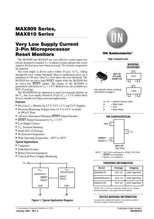
MAX809 Series,MAX810 SeriesVery Low Supply Current 3-Pin Microprocessor Reset MonitorsThe MAX809 and MAX810 are cost–effective system supervisor circuits designed to monitor V CC in digital systems and provide a reset signal to the host processor when necessary. No external components are required.The reset output is driven active within 10 µsec of V CC falling through the reset voltage threshold. Reset is maintained active for a minimum of 140 msec after V CC rises above the reset threshold. The MAX810 has an active–high RESET output while the MAX809 has an active–low RESET output. The output of the MAX809 is guaranteed valid down to V CC = 1.0 V. Both devices are available in a SOT–23 package.The MAX809/810 are optimized to reject fast transient glitches on the V CC line. Low supply current of 1.0 µA (V CC= 3.2 V) makes these devices suitable for battery powered applications.Features•Precision V CC Monitor for 2.5 V, 3.0 V, 3.3 V, and 5.0 V Supplies •Precision Monitoring V oltages from 1.6 V to 4.9 V Availablein 100 mV Steps•140 msec Guaranteed Minimum RESET Output Duration •RESET Output Guaranteed to V CC = 1.0 V•Low Supply Current•V CC Transient Immunity•Small SOT–23 Package•No External Components•Wide Operating Temperature: –40°C to 105°CTypical Applications•Computers•Embedded Systems•Battery Powered Equipment•Critical µP Power Supply MonitoringV CCFigure 1. Typical Application DiagramDevice Package ShippingORDERING INFORMATIONMAX809xTR SOT–233000 Tape/Reel MAX809SNxxxT1SOT–233000 Tape/Reel NOTE:*SOT–23 is equivalent to JEDEC (TO–236) **RESET is for MAX809***RESET is for MAX810SOT–23(TO–236)CASE 318PIN CONFIGURATION312V CCGNDRESET**SOT–23*(Top View)xx, xxx= Specific Device Codem= Date Codey= Yearw= Work WeekMARKINGDIAGRAMS32xxxm1(RESET)***MAX810xTR SOT–233000 Tape/ReelSee general marking information in the device marking section on page 8 of this data sheet.DEVICE MARKING INFORMATION NOTE: The “x” and “xxx” denotes a suffix for V cc voltage threshold options – see page 8 for more details.32xxyw1See specific device markinginformation on page 8.PIN DESCRIPTIONABSOLUTE MAXIMUM RATINGS* (Note 1)1.This device series contains ESD protection and exceeds the following tests:Human Body Model 2000 V per MIL–STD–883, Method 3015. Machine Model Method 350 V.2.The maximum package power dissipation limit must not be exceeded.P D +T J(max)*T Aq JAwith T J(max) = 150°C ELECTRICAL CHARACTERISTICS T A = –40°C to +105°C unless otherwise noted. Typical values are at T A = +25°C. (Note 3)The following data is given for MAX809 threshold levels: 1.60 V, 2.32 V, 2.93 V, 4.63 V and 4.90 V.AELECTRICAL CHARACTERISTICS(continued) T A = –40°C to +105°C unless otherwise noted. Typical values are at T A = +25°C. (Note 4) The following data is given for MAX809 threshold levels: 1.60 V, 2.32 V, 2.93 V, 4.63 V and 4.90 V.A5.Contact your ON Semiconductor sales representative for other threshold voltage options.ELECTRICAL CHARACTERISTICS (V CC = Full Range, T A = –40°C to +85°C unless otherwise noted. Typical values are at T A = +25°C, V CC = 5.0 V for L/M/J, 3.3 V for T/S, 3.0 V for R) (Note 6) The following data is given for MAX809 threshold levels: 2.63 V, 3.08 V, 4.00 V and 4.38 V; MAX810 threshold levels: 2.63 V, 2.93 V, 3.08 V, 4.38 V and 4.63 V.AAPPLICATIONS INFORMATIONV CC Transient RejectionThe MAX809 provides accurate V CC monitoring and reset timing during power–up, power–down, and brownout/sag conditions, and rejects negative–going transients (glitches)on the power supply line. Figure 2 shows the maximum transient duration vs. maximum negative excursion (overdrive) for glitch rejection. Any combination of duration and overdrive which lies under the curve will not generate a reset signal. Combinations above the curve are detected as a brownout or power–down. Typically, transient that goes 100 mV below the reset threshold and lasts 5 µs or less will not cause a reset pulse. Transient immunity can be improved by adding a capacitor in close proximity to the V CC pin of the MAX809.Figure 2. Maximum Transient Duration vs. Overdrivefor Glitch Rejection at 25°CV CC10.010080110.060.0M A X I M U M T R A N S I E N T D U R A T I O N (µs e c )20120RESET COMPARATOR OVERDRIVE (mV)160.06040RESET Signal Integrity During Power–DownThe MAX809 RESET output is valid to V CC = 1.0 V .Below this voltage the output becomes an “open circuit” and does not sink current. This means CMOS logic inputs to the µP will be floating at an undetermined voltage. Most digital systems are completely shutdown well above this voltage.However, in situations where RESET must be maintainedvalid to V CC = 0 V , a pull–down resistor must be connected from RESET to ground to discharge stray capacitances and hold the output low (Figure 3). This resistor value, though not critical, should be chosen such that it does not appreciably load RESET under normal operation (100 k W will be suitable for most applications).Figure 3. Ensuring RESET Valid to V CC = 0 VProcessors With Bidirectional I/O PinsSome µP’s (such as Motorola 68HC11) have bi–directional reset pins. Depending on the current drive capability of the processor pin, an indeterminate logic level may result if there is a logic conflict. This can be avoided by adding a 4.7 k W resistor in series with the output of the MAX809 (Figure 4). If there are other components in the system which require a reset signal, they should be buffered so as not to load the reset line. If the other components are required to follow the reset I/O of the µP, the buffer should be connected as shown with the solid line.Figure 4. Interfacing to Bidirectional Reset I/OBUFFERED RESETTYPICAL CHARACTERISTICSThe following data is given for MAX809 threshold levels: 1.60 V, 2.32 V, 2.93 V, 4.63 V and 4.90 V.1.10S U P P L Y C U R R E N T I N M I C R O A M PTEMPERATURE (°C)N O R M A L I Z E D P O W E R –U P R E S E T T I M E O U T–404020–206080Figure 7. Normalized Power–Up Reset vs.Temperature Figure 8. Normalized Reset Threshold Voltagevs. TemperatureTEMPERATURE (°C)–404020–206080TYPICAL CHARACTERISTICSThe following data is given for MAX809 threshold levels: 2.63 V, 3.08 V, 4.00 V and 4.38 V;MAX810 threshold levels: 2.63 V, 2.93 V, 3.08 V, 4.38 V and 4.63 V.S U P P L Y C U R R E N T ( A )m 040206080100P O W E R -D O W N R E S E T D E L A Y ( s e c )m TEMPERATURE (C °)-40-200204085Figure 13. Power–Up Reset Timeout vs.Temperature TEMPERATURE (C °)-40-20020406085225235230240245250P O W E R -U P R E S E T T I M E O U T (m s e c )60Figure 14. Normalized Reset Threshold vs.TemperatureTAPING FORMComponent Taping Orientation for 3L SOT–23 (JEDEC–236) Devices(Mark Right Side Up)SOT–23Package Carrier Width (W)Pitch (P)Part Per Full ReelReel Size 8 mm4 mm30007 inchesTape & Reel Specifications TableMARKING AND THRESHOLD INFORMATIONm = Date Codey = Yearw = Work WeekPACKAGE DIMENSIONSSOT–23PLASTIC PACKAGE (TO–236)CASE 318–08ISSUE AHNOTES:1.DIMENSIONING AND TOLERANCING PER ANSI Y14.5M, 1982.2.CONTROLLING DIMENSION: INCH.3.MAXIMUM LEAD THICKNESS INCLUDES LEADNotesNotes11ON Semiconductor and are trademarks of Semiconductor Components Industries, LLC (SCILLC). SCILLC reserves the right to make changes without further notice to any products herein. SCILLC makes no warranty, representation or guarantee regarding the suitability of its products for any particular purpose, nor does SCILLC assume any liability arising out of the application or use of any product or circuit, and specifically disclaims any and all liability, including without limitation special, consequential or incidental damages. “Typical” parameters which may be provided in SCILLC data sheets and/or specifications can and do vary in different applications and actual performance may vary over time. All operating parameters, including “Typicals” must be validated for each customer application by customer’s technical experts. SCILLC does not convey any license under its patent rights nor the rights of others.SCILLC products are not designed, intended, or authorized for use as components in systems intended for surgical implant into the body, or other applications intended to support or sustain life, or for any other application in which the failure of the SCILLC product could create a situation where personal injury or death may occur. Should Buyer purchase or use SCILLC products for any such unintended or unauthorized application, Buyer shall indemnify and hold SCILLC and its officers, employees, subsidiaries, affiliates, and distributors harmless against all claims, costs, damages, and expenses, and reasonable attorney fees arising out of, directly or indirectly, any claim of personal injury or death associated with such unintended or unauthorized use, even if such claim alleges that SCILLC was negligent regarding the design or manufacture of the part. SCILLC is an Equal Opportunity/Affirmative Action Employer. PUBLICATION ORDERING INFORMATIONJAPAN: ON Semiconductor, Japan Customer Focus Center4–32–1 Nishi–Gotanda, Shinagawa–ku, Tokyo, Japan 141–0031Phone: 81–3–5740–2700Email: r14525@This datasheet has been downloaded from:Free DownloadDaily Updated Database100% Free Datasheet Search Site100% Free IC Replacement Search SiteConvenient Electronic DictionaryFast Search SystemAll Datasheets Cannot Be Modified Without PermissionCopyright © Each Manufacturing Company。
MAX197使用指南MAX197芯片是多量程(±10V,±5V,0~10V,0~5V)、8通道、12位高精度的A/D转换器。
它采用逐次逼近工作方式,有标准的微机接口。
三态数据I/O口用做8位数据总线,数据总线的时序与绝大多数通用的微处理器兼容。
全部逻辑输入和输出与TTL/CMOS电平兼容。
新型A/D转换器芯片MAX197与一般A/D 转换器芯片相比,具有极好的性能价格比,仅需单一+5V供电,且外围电路简单,可简化电路设计。
1、特性(1)12位分辨率,1/2LSB线形度;(2)单+5V供电;(3)软件可编程选择输入量程:10V,5V,0~+5V,0~+10V;(4)输入多路选择器保护:16.5V(5)8路模拟输入通道;(6)6us转换时间,100kSPS采样速度;(7)内/外部采集控制;(8)内部4.096V或外部参考电压;(9)两种掉电模式;(10)内部或外部时钟。
2、2、引脚功能介绍MAX197具有四种不同的封装:DIP28,宽SO,SSOP和陶瓷SB封装。
1脚(CLK):时钟输入。
外部时钟输入时,由此引脚输入电平与TTL或CMOS兼容的时钟。
内部时钟模式时,该脚与地之间接一电容,以确定内部时钟频率,当f=1.56MHz时,外接电容的典型值CCLK=100PF。
2脚(CS):片选线,低电平有效。
3脚(WR):当为低电平时,在内部采集模式下,的上升沿将锁存数据,并启动一次采集和一次转换周期;在外部采集模式下,的第一个上升沿启动采集,第二个上升沿结束采集,并启动转换周期。
4脚(RD)当为低电平时,得下降沿将允许读取数据总线上的数据。
5脚(HBEN)用于切换12位转换结果。
此脚为高电平时数据总线上的数据为高4位,此脚为低电平时数据总上的数据为低8位。
*MAX197在多通道数据采集中的应⽤摘要:本文阐述了MAX197模数转换芯片的特性和工作原理,并结合其在多通道数据采集中的应用介绍了MCS-51系列单片机与MAX197的硬件接口设计和软件编程方法。
用于Peltier模块的集成温度控制器概论MAX1978 / MAX1979是用于Peltier热电冷却器(TEC)模块的最小, 最安全, 最精确完整的单芯片温度控制器。
片上功率FET和热控制环路电路可最大限度地减少外部元件, 同时保持高效率。
可选择的500kHz / 1MHz开关频率和独特的纹波消除方案可优化元件尺寸和效率, 同时降低噪声。
内部MOSFET的开关速度经过优化, 可降低噪声和EMI。
超低漂移斩波放大器可保持±0.001°C的温度稳定性。
直接控制输出电流而不是电压, 以消除电流浪涌。
独立的加热和冷却电流和电压限制提供最高水平的TEC保护。
MAX1978采用单电源供电, 通过在两个同步降压调节器的输出之间偏置TEC, 提供双极性±3A输出。
真正的双极性操作控制温度, 在低负载电流下没有“死区”或其他非线性。
当设定点非常接近自然操作点时, 控制系统不会捕获, 其中仅需要少量的加热或冷却。
模拟控制信号精确设置TEC 电流。
MAX1979提供高达6A的单极性输出。
提供斩波稳定的仪表放大器和高精度积分放大器, 以创建比例积分(PI)或比例积分微分(PID)控制器。
仪表放大器可以连接外部NTC或PTC热敏电阻, 热电偶或半导体温度传感器。
提供模拟输出以监控TEC温度和电流。
此外, 单独的过热和欠温输出表明当TEC温度超出范围时。
片上电压基准为热敏电阻桥提供偏置。
MAX1978 / MAX1979采用薄型48引脚薄型QFN-EP 封装, 工作在-40°C至+ 85°C温度范围。
采用外露金属焊盘的耐热增强型QFN-EP封装可最大限度地降低工作结温。
评估套件可用于加速设计。
应用光纤激光模块典型工作电路出现在数据手册的最后。
WDM, DWDM激光二极管温度控制光纤网络设备EDFA光放大器电信光纤接口ATE特征♦尺寸最小, 最安全, 最精确完整的单芯片控制器♦片上功率MOSFET-无外部FET♦电路占用面积<0.93in2♦回路高度<3mm♦温度稳定性为0.001°C♦集成精密积分器和斩波稳定运算放大器♦精确, 独立的加热和冷却电流限制♦通过直接控制TEC电流消除浪涌♦可调节差分TEC电压限制♦低纹波和低噪声设计♦TEC电流监视器♦温度监控器♦过温和欠温警报♦双极性±3A输出电流(MAX1978)♦单极性+ 6A输出电流(MAX1979)订购信息* EP =裸焊盘。
_______________General DescriptionThe MAX9690 is an ultra-fast ECL comparator manufac-tured with a high-frequency bipolar process (f T = 6GHz)capable of very short propagation delays. This design maintains the excellent DC matching characteristics nor-mally found only in slower comparators. The MAX9690 is similar in function to the MAX9685, except the latch-enable input is eliminated.The MAX9690 is pin-compatible with the CMP-08 but exceeds the AC characteristics of that device.The MAX9690 has differential inputs and complemen-tary outputs that are fully compatible with ECL-logic lev-els. Output current levels are capable of driving 50Ωterminated transmission lines. The ultra-fast operation makes signal processing possible at frequencies in excess of 600MHz.________________________ApplicationsHigh-Speed A/D Converters High-Speed Line Receivers Peak Detectors Threshold Detectors____________________________Featureso 1.3ns Propagation Delay o +5V, -5.2V Power Supplies o Pin-Compatible with CMP-08o Available in Commercial, Extended-Industrial,and Military Temperature Ranges o Available in Small-Outline PackageMAX9690Ultra-Fast ECL-Output Comparator________________________________________________________________Maxim Integrated Products 1__________________Pin Configuration______________Ordering Information________________Functional Diagram 19-2401; Rev 3; 3/97For free samples & the latest literature: , or phone 1-800-998-8800.For small orders, phone 408-737-7600 ext. 3468.M A X 9690Ultra-Fast ECL-Output Comparator 2_______________________________________________________________________________________ABSOLUTE MAXIMUM RATINGSELECTRICAL CHARACTERISTICS(V+ = +5V, V- = -5.2V, R L = 50Ω, V T = -2V, T A = +25°C, unless otherwise noted.)Stresses beyond those listed under “Absolute Maximum Ratings” may cause permanent damage to the device. These are stress ratings only, and functional operation of the device at these or any other conditions beyond those indicated in the operational sections of the specifications is not implied. Exposure to absolute maximum rating conditions for extended periods may affect device reliability.Supply Voltages.....................................................................±6V Input Voltages........................................................................±5V Differential Input Voltages...................................................±3.5V Output Current....................................................................30mA Continuous Power Dissipation (T A = +70°C)Plastic DIP (derate 9.09mW/°C above +70°C)...........727mW SO (derate 5.88mW/°C above +70°C).......................471mW CERDIP (derate 8.00mW/°C above +70°C)...............640mWOperating Temperature RangesMAX9690C_ A...................................................0°C to +70°C MAX9690E_ A................................................-40°C to +85°C MAX9690MJA..............................................-55°C to +125°C Storage Temperature Range.............................-55°C to +150°C Lead Temperature (soldering, 10sec).............................+300°CMAX9690Ultra-Fast ECL-Output Comparator_______________________________________________________________________________________3__________Applications InformationLayoutBecause of the MAX9690’s large gain-bandwidth charac-teristic, special precautions need to be taken if its high-speed capabilities are to be used. A PC board with a ground plane is mandatory. Mount all decoupling capac-itors as close to the power-supply pins as possible, and process the ECL outputs in microstrip fashion, consistent with the load termination of 50Ωto 120Ω. For low-imped-ance applications, microstrip layout at the input may also be helpful. Pay close attention to the bandwidth of the decoupling and terminating components. Chip compo-nents can be used to minimize lead inductance.Input Slew-Rate RequirementsAs with all high-speed comparators, the high gain-band-width product of these devices creates oscillation prob-lems when the input traverses through the linear region.For clean switching without oscillation or steps in the out-put waveform, the input must meet certain minimum slew-rate requirements. The tendency of the part to oscillate is a function of the layout and source impedance of the cir-cuit employed. Both poor layout and larger source imped-ance increase the minimum slew-rate requirement.____________________Timing DiagramThe timing diagram illustrates the series of events that completes the compare function, under worst-case conditions. The leading edge of the input signal (illus-trated as a large-amplitude, small-overdrive pulse)switches the comparator. Outputs –Q –and Q are similar in timing.Definition of TermsV OSInput Offset Voltage—The voltage required between the input terminals to obtain 0V differ-ential at the output.V IN Input Voltage Pulse Amplitude V OD Input Voltage Overdrivet pd+Input to Output High Delay—The propagation delay measured from the time the input signal crosses the input offset voltage to the 50% point of an output low-to-high transition.t pd-Input to Output Low Delay—The propagation delay measured from the time the input signal crosses the input offset voltage to the 50% point of an output high-to-low transition.SWITCHING CHARACTERISTICS(V+ = +5V, V- = -5.2V, R L = 50Ω, V T = -2V, T A = +25°C, unless otherwise noted.)Note 2:V IN = 100mV, V OD = 10mV.M A X 9690Ultra-Fast ECL-Output ComparatorFigure 1. Timing DiagramMaxim cannot assume responsibility for use of any circuitry other than circuitry entirely embodied in a Maxim product. No circuit patent licenses are implied. Maxim reserves the right to change the circuitry and specifications without notice at any time.4_____________________Maxim Integrated Products, 120 San Gabriel Drive, Sunnyvale, CA 94086 408-737-7600©1997 Maxim Integrated ProductsPrinted USAis a registered trademark of Maxim Integrated Products.。
_______________________________________________________________ Maxim Integrated Products 1For pricing, delivery, and ordering information, please contact Maxim Direct at 1-888-629-4642, or visit Maxim’s website at .250MHz to 4000MHz Dual,Analog Voltage Variable AttenuatorMAX1979019-5165; Rev 0; 3/10General DescriptionThe MAX19790 dual, general-purpose analog voltage variable attenuator (VVA) is designed to interface with 50I systems operating in the 250MHz to 4000MHz fre-quency range. Each attenuator includes a control circuit that provides 22dB of attenuation range with a linear control slope of 10dB/V.Both attenuators share a common analog control and can be cascaded together to yield 44dB of total dynamic range, with a combined linear control slope of 20dB/V.The IC is a monolithic device designed on one of Maxim’s proprietary SiG e BiCMOS processes. The device oper-ates from a single +5.0V supply and is available in a com-pact, 36-pin thin QFN package (6mm x 6mm x 0.8mm) with an exposed pad. Electrical performance is guaran-teed over the extended -40° to +85°C temperature range.ApplicationsBroadband System Applications, Including Wireless Infrastructure Digital and Spread-Spectrum Communication SystemsWCDMA/LTE, TD-SCDMA/TD-LTE, WiMAX™, cdma2000®, GSM/EDGE, and MMDS Base StationsVSAT/Satellite Modems Microwave Terrestrial Links Lineup Gain TrimTemperature Compensation Circuits Automatic Level Control (ALC)Transmitter Gain Control Receiver Gain Control General Test EquipmentFeaturesS 250MHz to 4000MHz RF Frequency Range S Integrates Two Analog Attenuators in One Monolithic Device S Flexible Attenuation-Control Ranges22dB (per Attenuator)44dB (Both Attenuators Cascaded)S 2.4dB 1500MHz Insertion Loss (per Attenuator)S Linear dB/V Analog Control Response Curve Simplifies Automatic Leveling Control and Gain-Trim Algorithms S Excellent Attenuation Flatness Over Wide Frequency Ranges and Attenuation Settings S Low 7.3mA Supply Current S Single +5.0V Supply VoltageOrdering Information+Denotes a lead(Pb)-free/RoHS-compliant package.*EP = Exposed pad.T = Tape and reel.WiMAX is a trademark of WiMAX Forum.cdma2000 is a registered trademark of TelecommunicationsIndustry Association.PART TEMP RANGE PIN-PACKAGE MAX19790ETX+-40N C to +85N C36 Thin QFN-EP*MAX19790ETX+T -40N C to +85N C36 Thin QFN-EP*250MHz to 4000MHz Dual,Analog Voltage Variable Attenuator M A X 197902Stresses beyond those listed under “Absolute Maximum Ratings” may cause permanent damage to the device. These are stress ratings only, and functional operation of the device at these or any other conditions beyond those indicated in the operational sections of the specifications is not implied. Exposure to absolute maximum rating conditions for extended periods may affect device reliability.V CC to GND ..........................................................-0.3V to +5.5V CTRL to GND (with V CC = +5.0V applied) ............0V to +4.75V All Other Pins to GND .................................-0.3V to V CC + 0.3V RF Input .........................................................................+20dBm Current into CTRL Pin (V CC grounded) .............................40mA Maximum Junction Temperature .....................................+150°C Operating Temperature Range ..........................-40°C to +85°CStorage Temperature Range ........................….-65°C to +150°C Continuous Power Dissipation (T C = +85°C) (Note 1) .......2.1W θJC (Notes 2, 4) ............................................................+10°C/W θJA (Notes 3, 4) ............................................................+35°C/W Lead Temperature (soldering, 10s) ................................+300°C Soldering Temperature (reflow) ......................................+260°CDC ELECTRICAL CHARACTERISTICS(V CC = +4.75V to +5.25V, V CTRL = +1.0V to +4.0V, no RF signals applied, all input and output ports terminated with 50I , T C = -40°C to +85°C, unless otherwise noted. Typical values are at V CC = +5.0V, V CTRL = +1.0V, T C = +25°C, unless otherwise noted.)RECOMMENDED AC OPERATING CONDITIONSABSOLUTE MAXIMUM RATINGSNote 1: T C is the temperature on the exposed pad of the package. T A is the ambient temperature of the device and PCB.Note 2: Based on junction temperature T J = T C + (θJC x V CC x I CC ). This formula can be used when the temperature of the exposedpad is known while the device is soldered down to a PCB. See the Applications Information section for details. The junction temperature must not exceed +150°C.Note 3: Junction temperature T J = T A + (θJA x V CC x I CC ). This formula can be used when the ambient temperature of the PCB isknown. The junction temperature must not exceed +150°C.Note 4: Package thermal resistances were obtained using the method described in JEDEC specification JESD51-7, using a four-layer board. For detailed information on package thermal considerations, refer to /thermal-tutorial.PARAMETERSYMBOLCONDITIONSMINTYPMAXUNITSSUPPLY Supply Voltage V CC 4.755.0 5.25V Supply Current I CC7.39.5mACONTROL INPUT Control Voltage Range V CTRL (Note 5)1.0 4.0V Control Input ResistanceR CTRL50k IPARAMETERSYMBOL CONDITIONSMIN TYPMAX UNITS RF Frequency Rangef RF(Note 6)2504000MHz250MHz to 4000MHz Dual,Analog Voltage Variable AttenuatorMAX197903AC ELECTRICAL CHARACTERISTICS(MAX19790 Evaluation Kit , line and connector losses included, two attenuators in cascade , V CC = 4.75V to 5.25V, RF ports are driven from 50I sources, input P RF = -10dBm, f RF = 950MHz to 2150MHz, V CTRL = +1.0V, T C = -40°C to +85°C. Typical values are for T C = +25°C, V CC = +5.0V, input P RF = -10dBm, f RF = 1500MHz, V CTRL = +1.0V, unless otherwise noted.)Note 5: Operating outside this range for extended periods may affect device reliability. Limit pin input current to 40mA when V CCis not present (see Table 1 for R4 value).Note 6: Operation outside this range is possible, but with degraded performance of some parameters. See the Typical OperatingCharacteristics .Note 7: f 1 = 1500MHZ, f 2 = 1501MHz, -10dBm/tone at attenuator input.Note 8: Guaranteed by design and characterization.Note 9: Switching time is measured from 50% of the control signal to when the RF output settles to Q 1dB.PARAMETERSYMBOLCONDITIONSMINTYP MAX UNITS Insertion LossILT C = +25N C950MHz to 1500MHz 4.4 6.3dB 950MHz to 2150MHz4.47.0Loss Variation Over Temperature T C = -40N C to +85N C0.6dB Input P 1dBIP 1dB 23.1dBm Input Second-Order Intercept PointIIP2f RF1 + f RF2 term, f RF1 - f RF2 = 1MHz (Note 7)69.6dBm Input Third-Order Intercept Point IIP3f RF1 - f RF2 = 1MHz (Note 7)36.3dBm Second Harmonic 2f IN 72dBc Third Harmonic3f IN77dBcAttenuation-Control RangeA ROne attenuator, V CTRL = +1.0V to +4.0V, T C = +25N C22dBTwo attenuators, V CTRL = +1.0V to +4.0V, T C = +25N C950MHz to 1500MHz 3644.7950MHz to 2150MHz3344.7Average Attenuation-Control SlopeV CTRL = +1.0V to +3.5V 20.0dB/V Maximum Attenuation-Control SlopeV CTRL = +1.0V to +3.5V30.4dB/V Attenuation Flatness Over 125MHz Bandwidth (Note 8)Peak-to-peak for V CTRL = +1.0V to +3.1V, T C = +25N C0.130.89dB Switching Time From 15dB to 0dB attenuation (Note 9)500ns Input Return Loss All gain settings 25dB Output Return Loss All gain settings21dB Group DelayInput/output 50I lines deembedded 190ps Group-Delay Flatness Over 125MHz Bandwidth Peak-to-peak10ps Group-Delay Change vs. Attenuation ControlV CTRL = +1.0V to +4.0V -175ps Insertion Phase Change vs. Attenuation ControlV CTRL = +1.0V to +4.0V82Degrees250MHz to 4000MHz Dual,Analog Voltage Variable Attenuator M A X 197904Typical Operating Characteristics(MAX19790 Evaluation Kit , two attenuators in cascade , V CC = +5.0V, P RF = -10dBm, T C = +25N C, V CTRL = +1.0V, unless otherwise noted.)SUPPLY CURRENT vs. V CCV CC (V)S U P P L Y C U R R E N T (m A )5.1255.0004.8757.07.58.06.54.7505.250INPUT MATCH vs. RF FREQUENCYRF FREQUENCY (MHz)S 11 (d B )300020001000-30-20-100-404000OUTPUT MATCH vs. RF FREQUENCYRF FREQUENCY (MHz)S 22 (d B )300020001000-30-20-100-404000INSERTION LOSS vs. RF FREQUENCYRF FREQUENCY (MHz)I N S E R T I O N L O S S (d B )30002000100024681012004000INPUT MATCH vs. V CTRLV CTRL (V)S 11 (d B)32-30-20-10-4014OUTPUT MATCH vs. V CTRLV CTRL (V)S 22 (d B)32-30-20-10-4014ATTENUATION vs. V CTRLV CTRL (V)S 21 (d B)32-50-40-30-20-10-6014ATTENUATION vs. V CTRLV CTRL (V)S 21 (d B )32-50-40-30-20-100-6014S21 PHASE CHANGE vs. V CTRLV CTRL (V)S 21 P H A S E C H A N G E (D E G )3250100150200-5014250MHz to 4000MHz Dual,Analog Voltage Variable AttenuatorMAX197905Typical Operating Characteristics (continued)(MAX19790 Evaluation Kit , two attenuators in cascade , V CC = +5.0V, P RF = -10dBm, T C = +25N C, V CTRL = +1.0V, unless otherwise noted.)INPUT IP3 vs. V CTRLV CTRL (V)I N P U T I P 3 (d B m )3225303540452014INPUT IP2 vs. V CTRLV CTRL (V)I N P U T I P 2 (d B m )3250607080904014INPUT IP2 vs. V CTRLV CTRL (V)I N P U T I P 2 (d B m )3250607080904014INPUT P 1dB vs. RF FREQUENCYRF FREQUENCY (MHz)I N P U T P 1d B (d B m )17501350212223242526209502150INPUT IP3 vs. VCTRLV CTRL (V)I N P U T I P 3 (d B m )3225303540452014INPUT P 1dB vs. RF FREQUENCYRF FREQUENCY (MHz)I N P U T P 1d B (d B m )17501350212223242526209502150250MHz to 4000MHz Dual,Analog Voltage Variable Attenuator M A X 197906Typical Operating Characteristics (continued)(MAX19790 Evaluation Kit , one attenuator connected , V CC = +5.0V, P RF = -10dBm, T C = +25N C, V CTRL = +1.0V, unless otherwise noted.)ATTENUATION vs. V CTRLV CTRL (V)S 21 (d B )32-25-20-15-10-50-3014OUTPUT MATCH vs. RF FREQUENCYRF FREQUENCY (MHz)S 22 (d B )300020001000-40-30-20-100-5004000SUPPLY CURRENT vs. V CCV CC (V)S U P P L Y C U R R E N T (m A )5.1255.0004.8757.07.58.06.54.7505.250S21 PHASE CHANGE vs. V CTRLV CTRL (V)S 21 P H A S E C H A N G E (D E G R E E S )32-250255075100-5014INSERTION LOSS vs. RF FREQUENCYRF FREQUENCY (MHz)I N S E R T I O N L O S S (d B )3000200010002468004000INPUT MATCH vs. RF FREQUENCYRF FREQUENCY (MHz)S 11 (d B )300020001000-40-30-20-100-504000INPUT MATCH vs. V CTRLV CTRL (V)S 11 (d B )32-40-30-20-100-5014OUTPUT MATCH vs. V CTRLV CTRL (V)S 22 (d B )32-40-30-20-100-5014ATTENUATION vs. V CTRLV CTRL (V)S 21 (d B )32-25-20-15-10-50-3014250MHz to 4000MHz Dual,Analog Voltage Variable AttenuatorMAX197907Typical Operating Characteristics (continued)(MAX19790 Evaluation Kit , one attenuator connected , V CC = +5.0V, P RF = -10dBm, T C = +25N C, V CTRL = +1.0V, unless otherwise noted.)INPUT IP3 vs. V CTRLV CTRL (V)I N P U T I P 3 (d B m )3225303540452014INPUT IP2 vs. V CTRLV CTRL (V)I N P U T I P 2 (d B m )32607080901005014INPUT IP3 vs. V CTRLV CTRL (V)I N P U T I P 3 (d B m )3225303540452014INPUT IP2 vs. V CTRLV CTRL (V)I N P U T I P 2 (d B m )32607080901005014INPUT P 1dB vs. RF FREQUENCYRF FREQUENCY (MHz)I N P U T P 1d B (d B m )17501350212223242526209502150INPUT P1dB vs. RF FREQUENCYRF FREQUENCY (MHz)I N P U T P 1d B (d B m )17501350212223242526209502150250MHz to 4000MHz Dual,Analog Voltage Variable Attenuator M A X 197908Pin DescriptionPin Configuration/Functional DiagramPINNAME DESCRIPTION1, 3, 4, 6, 7, 9, 10,12, 14–28, 30, 31,33, 34, 36GNDGround. Connect to the board’s ground plane using low-inductance layout techniques.2OUT_A Attenuator A Output. Internally matched to 50I over the operating frequency band. This pin, if used, requires a DC block. If this attenuator is not used, the pin can be left unconnected.5, 13, 32V CC Power Supply. Bypass to GND with capacitors and resistors as shown in the Typical Application Circuit .8IN_AAttenuator A Input. Internally matched to 50I over the operating frequency band. This pin, if used, requires a DC block. If this attenuator is not used, the pin can be left unconnected.11CTRLAnalog Attenuator Control Input. V CC must be present unless using a current-limiting resis-tor, as noted in the Applications Information section. Limit voltages applied to this pin to a +1.0V to +4.0V range with V CC present to ensure device reliability.29OUT_B Attenuator B Output. Internally matched to 50I over the operating frequency band. This pin, if used, requires a DC block. If this attenuator is not used, the pin can be left unconnected.35IN_B Attenuator B Input. Internally matched to 50I over the operating frequency band. This pin, if used, requires a DC block. If this attenuator is not used, the pin can be left unconnected.—EPExposed Pad. Internally connected to GND. Solder evenly to the board’s ground plane for proper operation.250MHz to 4000MHz Dual,Analog Voltage Variable AttenuatorMAX197909Detailed DescriptionThe MAX19790 is a dual, general-purpose analog volt-age variable attenuator (VVA) designed to interface with 50I systems operating in the 250MHz to 4000MHz frequency range. Each attenuator includes a control circuit that provides 22dB of attenuation range with a linear control slope of 10dB/V. Both attenuators share a common analog control and can be cascaded together to yield 44dB of total dynamic range, with a combined linear control slope of 20dB/V.Applications InformationAnalog Attenuation ControlA single input voltage at the CTRL pin adjusts the attenu-ation of the device. Up to 22dB of attenuation-control range is provided per attenuator. At the insertion-loss setting, the attenuator’s loss is approximately 2.4dB.If a larger attenuation-control range is desired, the second on-chip attenuator can be connected in series to provide an additional 22dB of gain-control range.Note that the CTRL pin simultaneously adjusts both on-chip attenuators. The CTRL input voltage drives a high-impedance load (> 50k I ). It is suggested that a current-limiting resistor be included in series with thisconnection, to limit the input current to less than 40mA, should the control voltage be applied when V CC is not present. A series resistor of greater than 200I provides complete protection for +5.0V control voltage ranges. Note: To ensure the reliability of the device, limit CTRL input voltages to a +1.0V to +4.0V range when V CC is present.Layout ConsiderationsA properly designed PCB is an essential part of any RF/microwave circuit. Keep RF signal lines as short as possible to reduce losses, radiation, and inductance. For best performance, route the ground-pin traces directly to the exposed pad underneath the package. This pad MUST be connected to the ground plane of the board by using multiple vias under the device to provide the best RF and thermal conduction path. Solder the exposed pad on the bottom of the device package to a PCB exposed pad.Power-Supply BypassingProper voltage-supply bypassing is essential for high-frequency circuit stability. Bypass each V CC pin with capacitors placed as close as possible to the device. Place the smallest capacitor closest to the device. See the Typical Application Circuit and Table 1 for details.T able 1. Typical Application Circuit Component Values *C8 can be used to provide additional filtering. Depending on the external driver used on the CTRL line, this capacitance could slow down the response time.DESIGNATION QTY DESCRIPTIONC1, C3, C53220pF Q 5%, 50V C0G ceramiccapacitors (0402)Murata GRM1555C1H221J C2, C420.01F F Q 10%, 25V X7R ceramic capacitors (0402)Murata GRM155R71E103K C611000pF Q 5%, 50V C0G ceramic capacitor (0402)Murata GRM1555C1H102J C710.1F F Q 10%, 16V X7R ceramic capacitor (0603)Murata GRM188R71C104K C8*0Not installed, ceramic capacitor (0603)DESIGNATIONQTY DESCRIPTIONC9122pF Q 5%, 50V C0G ceramic capacitor (0402)Murata GRM1555C1H220J R1, R2210I Q 5% resistors (0402)AnyR3, R420I resistors (0402)Note: In cases where V CTRL is applied before or removed after V CC , use R4 = 200I .U11Analog attenuator IC Maxim MAX19790ETX+Note: U1 has an exposed pad conductor, which requires it to be solder-attached to a grounded pad on the PCB to ensure aproper electrical/thermal design.250MHz to 4000MHz Dual,Analog Voltage Variable Attenuator M A X 1979010Typical Application CircuitExposed Pad RF and ThermalConsiderationsThe exposed pad (EP) of the device’s 36-pin thin QFN package provides a low thermal-resistance path to the die. It is important that the PCB on which the IC is mounted be designed to conduct heat from this contact. In addition, provide the EP with a low-inductance RF ground path for the device.The EP MUST be soldered to a ground plane on the PCB, either directly or through an array of plated via holes. Soldering the pad to ground is also critical for efficient heat transfer. Use a solid ground plane wherever possible.250MHz to 4000MHz Dual,Analog Voltage Variable Attenuator MAX19790Maxim cannot assume responsibility for use of any circuitry other than circuitry entirely embodied in a Maxim product. No circuit patent licenses are implied. Maxim reserves the right to change the circuitry and specifications without notice at any time.Maxim Integrated Products, 120 San Gabriel Drive, Sunnyvale, CA 94086 408-737-7600 11© 2010 Maxim Integrated Products Maxim is a registered trademark of Maxim Integrated Products, Inc. Package Information For the latest package outline information and land patterns,go to /packages . Note that a “+”, “#”, or“-” in the package code indicates RoHS status only. Packagedrawings may show a different suffix character, but the drawing pertains to the package regardless of RoHS status.Chip InformationPROCESS: BiCMOS。