XL1000-BD中文资料
- 格式:pdf
- 大小:952.44 KB
- 文档页数:7
28 26 24 22 20 18 16 14 12 10 8 6 4 2 0 18.0
XL1000 Vd=5.0 V Id=50 mA ~19,550 Devices
0 -5 -10 -15 -20 -25 -30 -35 -40 -45 -50 -55 -60 -65 -70 -75 18.0
Reverse Isolation (dB)
Gain (dB)
20.0
22.0
24.0
26.0
28.0
30.0
32.0
34.0
36.0
38.0
40.0
20.0
22.0
24.0
26.0
28.0
30.0
32.0
34.0
36.0
38.0
40.0
Frequency (GHz) Max Median Mean -3sigma
Frequency (GHz) +3sigma Median Mean -3sigma
30.0
32.0
34.0
36.0
38.0
40.0
Frequency (GHz) Max Median Mean -3sigma Max
Frequency (GHz) Median Mean -3sigma
XL1000 Vd=3.0 V Id=35 mA ~130 Devices
13.0
Output Power Psat (dBm)
XL1000 Vd=5.0 V Id=50 mA ~19,550 Devices
0
Output Return Loss (dB) Input Return Loss (dB)
XL1000 Vd=5.0 V Id=50 mA ~19,300 Devices
0 -5 -10 -15 -20 -25 -30 -35 -40 18.0
-5 -10 -15 -20 -25 -30 -35 -40 18.0
20.0
22.0
24.0
26.0
28.0
30.0
32.0
34.020.0
22.0
24.0
26.0
28.0
30.0
32.0
34.0
36.0
38.0
40.0
Frequency (GHz) Max Median Mean -3sigma Max
General Description
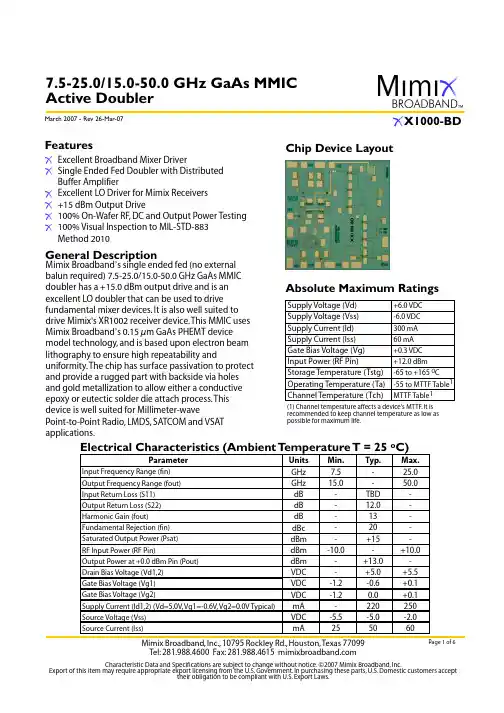
Mimix Broadband’s three stage 20.0-40.0 GHz GaAs MMIC low noise amplifier has a small signal gain of 20.0 dB with a noise figure of 2.0 dB across the band. This MMIC uses Mimix Broadband’s 0.15 µm GaAs PHEMT device model technology, and is based upon electron beam lithography to ensure high repeatability and uniformity. The chip has surface passivation to protect and provide a rugged part with backside via holes and gold metallization to allow either a conductive epoxy or eutectic solder die attach process. This device is well suited for Millimeter-wave Point-to-Point Radio, LMDS, SATCOM and VSAT applications.
Input Return Loss (dB)
XL1000 Vd=3.0 V Id=35 mA ~1000 Devices
0 -5 -10 -15 -20 -25 -30 18.0
20.0
22.0
24.0
26.0
28.0
30.0
32.0
34.0
36.0
38.0
40.0
20.0
22.0
24.0
26.0
28.0
5.0 4.5
Noise Figure (dB)
XL1000 Vd=3.0 V Id=35 mA ~100 Devices
12.0 11.0 10.0 9.0 8.0 7.0 6.0 5.0
4.0 3.5 3.0 2.5 2.0 1.5 1.0 0.5
4.0 3.0 18.0
0.0 18.0 20.0 22.0 24.0 26.0 28.0 30.0 32.0 34.0 36.0 38.0 40.0
+7.0 VDC 70 mA +12 dBm -65 to +165 OC -55 to MTTF Table 1 MTTF Table 1
(1) Channel temperature affects a device's MTTF. It is recommended to keep channel temperature as low as possible for maximum life.
Absolute Maximum Ratings
Supply Voltage (Vd) Supply Current (Id) Input Power (Pin) Storage Temperature (Tstg) Operating Temperature (Ta) Channel Temperature (Tch)
20.0-40.0 GHz GaAs MMIC Low Noise Amplifier
April 2005 - Rev 01-Apr-05
L1000
Low Noise Amplifier Measurements (cont.)
XL1000 Vd=5.0 V Id=50 mA ~19,300 Devices
20.0
22.0
24.0
26.0
28.0
30.0
32.0
34.0
36.0
38.0
40.0
Frequency (GHz) Max Median Mean -3sigma
Frequency (GHz) Max Median Mean -3sigma
Mimix Broadband, Inc., 10795 Rockley Rd., Houston, Texas 77099 Tel: 281.988.4600 Fax: 281.988.4615
Reverse Isolation (dB)
XL1000 Vd=3.0 V Id=35 mA ~1000 Devices
Gain (dB)
20.0
22.0
24.0
26.0
28.0
30.0
32.0
34.0
36.0
38.0
40.0
20.0
22.0
24.0
26.0
28.0
30.0
32.0
34.0
36.0
38.0
Electrical Characteristics (Ambient Temperature T = 25 oC)
Parameter Frequency Range (f ) Input Return Loss (S11) 2 @ 22.0-36.0 GHz Output Return Loss (S22) 2 @ 22.0-36.0 GHz Small Signal Gain (S21)2 Gain Flatness (∆S21) Reverse Isolation (S12) 2 Noise Figure (NF)2 @ 24.0-40.0 GHz Output Power for 1 dB Compression (P1dB) Output Third Order Intercept Point (OIP3) Drain Bias Voltage (Vd) Supply Current (Id) (Vd=3.0V or 5.0V)
Units GHz dB dB dB dB dB dB dBm dBm VDC mA Min. 20.0 6.0 4.0 12.0 30.0 Typ. 12.0 10.0 20.0 +/-4.0 45.0 2.0 +9.0 +16.0 +3.0 35 Max. 40.0 +5.0 50
(2) Unless otherwise indicated min/max over 20.0-40.0 GHz and biased at Vd=5V, Id=50mA.
Page 2 of 7
Characteristic Data and Specifications are subject to change without notice. ©2005 Mimix Broadband, Inc. Export of this item may require appropriate export licensing from the U.S. Government. In purchasing these parts, U.S. Domestic customers accept their obligation to be compliant with U.S. Export Laws.
20.0-40.0 GHz GaAs MMIC Low Noise Amplifier
April 2005 - Rev 01-Apr-05
XL1000 Vd=5.0 V Id=50 mA ~19,550 Devices
0 -5 -10 -15 -20 -25 -30 -35 -40 -45 -50 -55 -60 -65 -70 -75 18.0
Reverse Isolation (dB)
Gain (dB)
20.0
22.0
24.0
26.0
28.0
30.0
32.0
34.0
36.0
38.0
40.0
20.0
22.0
24.0
26.0
28.0
30.0
32.0
34.0
36.0
38.0
40.0
Frequency (GHz) Max Median Mean -3sigma
Frequency (GHz) +3sigma Median Mean -3sigma
30.0
32.0
34.0
36.0
38.0
40.0
Frequency (GHz) Max Median Mean -3sigma Max
Frequency (GHz) Median Mean -3sigma
XL1000 Vd=3.0 V Id=35 mA ~130 Devices
13.0
Output Power Psat (dBm)
XL1000 Vd=5.0 V Id=50 mA ~19,550 Devices
0
Output Return Loss (dB) Input Return Loss (dB)
XL1000 Vd=5.0 V Id=50 mA ~19,300 Devices
0 -5 -10 -15 -20 -25 -30 -35 -40 18.0
-5 -10 -15 -20 -25 -30 -35 -40 18.0
20.0
22.0
24.0
26.0
28.0
30.0
32.0
34.020.0
22.0
24.0
26.0
28.0
30.0
32.0
34.0
36.0
38.0
40.0
Frequency (GHz) Max Median Mean -3sigma Max
General Description
Mimix Broadband’s three stage 20.0-40.0 GHz GaAs MMIC low noise amplifier has a small signal gain of 20.0 dB with a noise figure of 2.0 dB across the band. This MMIC uses Mimix Broadband’s 0.15 µm GaAs PHEMT device model technology, and is based upon electron beam lithography to ensure high repeatability and uniformity. The chip has surface passivation to protect and provide a rugged part with backside via holes and gold metallization to allow either a conductive epoxy or eutectic solder die attach process. This device is well suited for Millimeter-wave Point-to-Point Radio, LMDS, SATCOM and VSAT applications.
Input Return Loss (dB)
XL1000 Vd=3.0 V Id=35 mA ~1000 Devices
0 -5 -10 -15 -20 -25 -30 18.0
20.0
22.0
24.0
26.0
28.0
30.0
32.0
34.0
36.0
38.0
40.0
20.0
22.0
24.0
26.0
28.0
5.0 4.5
Noise Figure (dB)
XL1000 Vd=3.0 V Id=35 mA ~100 Devices
12.0 11.0 10.0 9.0 8.0 7.0 6.0 5.0
4.0 3.5 3.0 2.5 2.0 1.5 1.0 0.5
4.0 3.0 18.0
0.0 18.0 20.0 22.0 24.0 26.0 28.0 30.0 32.0 34.0 36.0 38.0 40.0
+7.0 VDC 70 mA +12 dBm -65 to +165 OC -55 to MTTF Table 1 MTTF Table 1
(1) Channel temperature affects a device's MTTF. It is recommended to keep channel temperature as low as possible for maximum life.
Absolute Maximum Ratings
Supply Voltage (Vd) Supply Current (Id) Input Power (Pin) Storage Temperature (Tstg) Operating Temperature (Ta) Channel Temperature (Tch)
20.0-40.0 GHz GaAs MMIC Low Noise Amplifier
April 2005 - Rev 01-Apr-05
L1000
Low Noise Amplifier Measurements (cont.)
XL1000 Vd=5.0 V Id=50 mA ~19,300 Devices
20.0
22.0
24.0
26.0
28.0
30.0
32.0
34.0
36.0
38.0
40.0
Frequency (GHz) Max Median Mean -3sigma
Frequency (GHz) Max Median Mean -3sigma
Mimix Broadband, Inc., 10795 Rockley Rd., Houston, Texas 77099 Tel: 281.988.4600 Fax: 281.988.4615
Reverse Isolation (dB)
XL1000 Vd=3.0 V Id=35 mA ~1000 Devices
Gain (dB)
20.0
22.0
24.0
26.0
28.0
30.0
32.0
34.0
36.0
38.0
40.0
20.0
22.0
24.0
26.0
28.0
30.0
32.0
34.0
36.0
38.0
Electrical Characteristics (Ambient Temperature T = 25 oC)
Parameter Frequency Range (f ) Input Return Loss (S11) 2 @ 22.0-36.0 GHz Output Return Loss (S22) 2 @ 22.0-36.0 GHz Small Signal Gain (S21)2 Gain Flatness (∆S21) Reverse Isolation (S12) 2 Noise Figure (NF)2 @ 24.0-40.0 GHz Output Power for 1 dB Compression (P1dB) Output Third Order Intercept Point (OIP3) Drain Bias Voltage (Vd) Supply Current (Id) (Vd=3.0V or 5.0V)
Units GHz dB dB dB dB dB dB dBm dBm VDC mA Min. 20.0 6.0 4.0 12.0 30.0 Typ. 12.0 10.0 20.0 +/-4.0 45.0 2.0 +9.0 +16.0 +3.0 35 Max. 40.0 +5.0 50
(2) Unless otherwise indicated min/max over 20.0-40.0 GHz and biased at Vd=5V, Id=50mA.
Page 2 of 7
Characteristic Data and Specifications are subject to change without notice. ©2005 Mimix Broadband, Inc. Export of this item may require appropriate export licensing from the U.S. Government. In purchasing these parts, U.S. Domestic customers accept their obligation to be compliant with U.S. Export Laws.
20.0-40.0 GHz GaAs MMIC Low Noise Amplifier
April 2005 - Rev 01-Apr-05