allegro_PCB_SI仿真
- 格式:doc
- 大小:598.00 KB
- 文档页数:45
第一章在Allegro 中准备好进行SI 仿真的PCB 板图1)在Cadence 中进行SI 分析可以通过几种方式得到结果:* Allegro 的PCB 画板界面,通过处理可以直接得到结果,或者直接以*.brd 存盘。
* 使用Specctre Quest 打开*.brd,进行必要设置,通过处理直接得到结果。
这实际与上述方式类似,只不过是两个独立的模块,真正的仿真软件是下面的SigXplore 程序。
* 直接打开SigXplore 建立拓扑进行仿真。
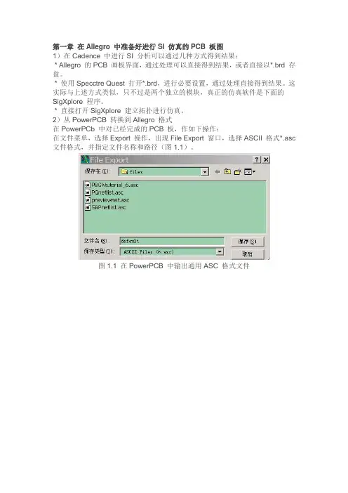
2)从PowerPCB 转换到Allegro 格式在PowerPCb 中对已经完成的PCB 板,作如下操作:在文件菜单,选择Export 操作,出现File Export 窗口,选择ASCII 格式*.asc 文件格式,并指定文件名称和路径(图1.1)。
图1.1 在PowerPCB 中输出通用ASC 格式文件图1.2 PowerPCB 导出格式设置窗口点击图1.1 的保存按钮后出现图1.2 ASCII 输出定制窗口,在该窗口中,点击“Select All”项、在Expand Attributes 中选中Parts 和Nets 两项,尤其注意在Format 窗口只能选择PowerPCB V3.0 以下版本格式,否则Allegro 不能正确导入。
3)在Allegro 中导入*.ascPCB 板图在文件菜单,选择Import 操作,出现一个下拉菜单,在下拉菜单中选择PADS 项,出现PADS IN 设置窗口(图1.3),在该窗口中需要设置3 个必要参数:图1.3 转换阿三次文件参数设置窗口i. 在的一栏那填入源asc 文件的目录ii. 在第二栏指定转换必须的pads_in.ini 文件所在目录(也可将此文件拷入工作目录中,此例)iii. 指定转换后的文件存放目录然后运行“Run”,将在指定的目录中生成转换成功的.brd 文件。
注:pads_in.ini 所在目录路:.Psd_14.2ToolsPCBbin 中。

Allegro后仿真流程介绍作成期:04/01/2009作成人:SOLDERMASKForewordGetting IBIS ModelsPre-WorkingSimulationView WaveformForeword●Getting IBIS Models ●Pre-Working Simulation●●View WaveformForeword前仿真和后仿真的区别前仿真又可以分为布局前仿真和布局后仿真。
前者是在设计的最初阶段,通过SigXplorer建立和验证详细的电气拓扑结构并以此制定出详细的约束规则。
后者是在布局完成的状态下,在布线过程中遇到的具体设计问题需要仿真的过程。
后仿真是在PCB布线完成以后,对已经完成的关键网络进行仿真验证的过程。
可以检查实际的物理执行过程(布局布线)是否违背设计意图;或是已知的改动,通过仿真来验证这种改动给高速设计带来的影响。
本篇文档主要介绍后仿真的操作流程Index●ForewordGetting IBIS Models●Pre-Working●Simulation●View Waveform到下列网站搜索各个公司IBIS模型下载网站/ibis/ibis%20table/models.htm到Google网站直接搜索某个型号的IBIS模型到器件厂商的官方网站下载IBIS模型需要检查是否存在语法错误,或者其他的错误,这一步是必须的。
打开软件Model Integrity,点击Open打开ibs文件,打开文件时软件自动进行Check。
若遇到错误,及时查明原因,一般都是语法错误,所以稍加修改就OK了。
点击此按钮查看报错的行并修改之有10个错误,原因是超出80字符IBIS to DML由于Allegro SI不能够直接对应IBIS模型,需要把IBIS模型转换成Allegro专用的DML模型,两者实际上都是文本文档,只是在描述的方式上有所区别。
右击,在弹出的框内选择IBIS to DML生成dml模型后保存至ibis模型同一路径待所有需要的器件模型全部转换成DML模型以后,要和IBIS模型保存在同一文件夹。
第一章在Allegro 中准备好进行SI 仿真的PCB 板图1)在Cadence 中进行SI 分析可以通过几种方式得到结果:* Allegro 的PCB 画板界面,通过处理可以直接得到结果,或者直接以*.brd 存盘。
* 使用Specctre Quest 打开*.brd,进行必要设置,通过处理直接得到结果。
这实际与上述方式类似,只不过是两个独立的模块,真正的仿真软件是下面的SigXplore 程序。
* 直接打开SigXplore 建立拓扑进行仿真。
2)从PowerPCB 转换到Allegro 格式在PowerPCb 中对已经完成的PCB 板,作如下操作:在文件菜单,选择Export 操作,出现File Export 窗口,选择ASCII 格式*.asc 文件格式,并指定文件名称和路径(图1.1)。
图1.1 在PowerPCB 中输出通用ASC 格式文件图1.2 PowerPCB 导出格式设置窗口点击图1.1 的保存按钮后出现图1.2 ASCII 输出定制窗口,在该窗口中,点击“Select All”项、在Expand Attributes 中选中Parts 和Nets 两项,尤其注意在Format 窗口只能选择PowerPCB V3.0 以下版本格式,否则Allegro 不能正确导入。
3)在Allegro 中导入*.ascPCB 板图在文件菜单,选择Import 操作,出现一个下拉菜单,在下拉菜单中选择PADS 项,出现PADS IN 设置窗口(图1.3),在该窗口中需要设置3 个必要参数:图1.3 转换阿三次文件参数设置窗口i. 在的一栏那填入源asc 文件的目录ii. 在第二栏指定转换必须的pads_in.ini 文件所在目录(也可将此文件拷入工作目录中,此例)iii. 指定转换后的文件存放目录然后运行“Run”,将在指定的目录中生成转换成功的.brd 文件。
注:pads_in.ini 所在目录路:.Psd_14.2ToolsPCBbin 中。

基于Cadence Allegro SI 16.3的信号完整性仿真信号完整性是指信号在信号线上的质量。
信号具有良好的信号完整性是指当在需要的时候,具有所必需达到的电压电平数值。
差的信号完整性不是由某一因素导致的,而是由板级设计中多种因素共同引起的。
特别是在高速电路中,所使用的芯片的切换速度过快、端接元件布设不合理、电路的互联不合理等都会引起信号的完整性问题。
具体主要包括串扰、反射、过冲与下冲、振荡、信号延迟等。
信号完整性问题由多种因素引起,归结起来有反射、串扰、过冲和下冲、振铃、信号延迟等,其中反射和串扰是引发信号完整性问题的两大主要因素。
反射和我们所熟悉的光经过不连续的介质时都会有部分能量反射回来一样,就是信号在传输线上的回波现象。
此时信号功率没有全部传输到负载处,有一部分被反射回来了。
在高速的PCB中导线必须等效为传输线,按照传输线理论,如果源端与负载端具有相同的阻抗,反射就不会发生了。
如果二者阻抗不匹配就会引起反射,负载会将一部分电压反射回源端。
根据负载阻抗和源阻抗的关系大小不同,反射电压可能为正,也可能为负。
如果反射信号很强,叠加在原信号上,很可能改变逻辑状态,导致接收数据错误。
如果在时钟信号上可能引起时钟沿不单调,进而引起误触发。
一般布线的几何形状、不正确的线端接、经过连接器的传输及电源平面的不连续等因素均会导致此类反射。
另外常有一个输出多个接收,这时不同的布线策略产生的反射对每个接收端的影响也不相同,所以布线策略也是影响反射的一个不可忽视的因素。
串扰是相邻两条信号线之间的不必要的耦合,信号线之间的互感和互容引起线上的噪声。
因此也就把它分为感性串扰和容性串扰,分别引发耦合电流和耦合电压。
当信号的边沿速率低于1ns时,串扰问题就应该考虑了。
如果信号线上有交变的信号电流通过时,会产生交变的磁场,处于磁场中的相邻的信号线会感应出信号电压。
一般PCB板层的参数、信号线间距、驱动端和接收端的电气特性及信号线的端接方式对串扰都有一定的影响。

Cadence PCB SI仿真流程——孙海峰高速高密度多层PCB板的SI/EMC(信号完整性/电磁兼容)问题长久以来一直是设计者所面对的最大挑战。
然而,随着主流的MCU、DSP和处理器大多工作在100MHz以上(有些甚至工作于GHz级以上),以及越来越多的高速I/O埠和RF前端也都工作在GHz级以上,再加上应用系统的小型化趋势导致的PCB 空间缩小问题,使得目前的高速高密度PCB板设计已经变得越来越普遍。
许多产业分析师指出,在进入21世纪以后,80%以上的多层PCB设计都将会针对高速电路。
高速讯号会导致PCB板上的长互连走线产生传输线效应,它使得PCB设计者必须考虑传输线的延迟和阻抗搭配问题,因为接收端和驱动端的阻抗不搭配都会在传输在线产生反射讯号,而严重影响到讯号的完整性。
另一方面,高密度PCB板上的高速讯号或频率走线则会对间距越来越小的相邻走线产生很难准确量化的串扰与EMC问题。
SI和EMC的问题将会导致PCB设计过程的反复,而使得产品的开发周期一再延误。
一般来说,高速高密度PCB需要复杂的阻抗受控布线策略才能确保电路正常工作。
随着新型组件的电压越来越低、PCB板密度越来越大、边缘转换速率越来越快,以及开发周期越来越短,SI/EMC挑战便日趋严峻。
为了达到这个挑战的要求,目前的PCB设计者必须采用新的方法来确保其PCB设计的可行性与可制造性。
过去的传统设计规则已经无法满足今日的时序和讯号完整性要求,而必须采取包含仿真功能的新款工具才足以确保设计成功。
Cadence的Allegro PCB SI提供了一种弹性化且整合的信号完整性问题解决方案,它是一种完整的SI/PI(功率完整性)/EMI问题的协同解决方案,适用于高速PCB设计周期的每个阶段,并解决与电气性能相关的问题。
Allegro PCB SI信号完整性分析的操作步骤,就是接下来将要介绍的。
一、Allegro PCB SI分析前准备:1、准备需要分析的PCB,如下图;2、SI分析前的相关设置,执行T ools/Setup Advisor,进入Database Setup Advisor 对话框,进行SI分析前的设置;(1)设置PCB叠层的材料、阻抗等,点击Edit Cross section,进入叠层阻抗等设置界面。
收稿日期:2002-04-03利用Cadence A llegro进行PCB级的信号完整性仿真Signa l I n tegr ity Si m ula tion w ith A llegro for PCB Board D esign李 新L i X in 张 琳Zhang L in(西安电子科技大学 西安 710071) (西安大唐电信有限公司 西安 710075)(X idian U niversity,X i′an,710071,Ch ina) (X i′an D atang Telecom,X i′an,710075,Ch ina)摘 要 在高速PCB设计过程中,仅仅依靠个人经验布线,往往存在巨大的局限性。
利用Cadence的A llegro软件包对电路进行PCB级的仿真,可以最优化线路布局,极大地提高电路设计质量,从而缩短设计周期。
本文结合作者的实际设计经验,介绍使用Cadence的一般步骤并列举在使用过程中所发现的一些问题。
关键词 高速PCB布线 A llegro文件转换 信号完整性仿真 随着信息宽带化和高速化的发展,以前的低速PCB已完全不能满足日益增长信息化发展的需要,而高速PCB的出现将对硬件人员提出更高的要求,仅仅依靠自己的经验去布线,会顾此失彼,造成研发周期过长,浪费财力物力,生产出来的产品不稳定。
一般认为高速PCB是指其数字信号边沿上升时间小于4倍信号传输时延,这种高速PCB的信号线必须按照传输线理论去设计,否则将会严重影响信号的完整性。
Cadence公司针对PCB D esign Studi o发布一个功能非常实用的高速电路设计及信号完整性分析的工具选件ALL EGRO PCB。
利用这个仿真软件能够根据叠层的排序,PCB的介电常数,介质的厚度,信号层所处的位置以及线宽等等来判断某一PCB线条是否属于微带线、带状线、宽带耦合带状线,并且根据不同的计算公式自动计算出信号线的阻抗以及信号的反射、串绕、电磁干扰等等,从而可以对布线进行约束以保证PCB的信号完整性。
Allegro PCB SI:一步一步学会前仿真Learn Allegro PCB SI Pre-simulation Step by StepDoc Scope : Cadence 16.5Doc Number : SFTEC12007Author : Daniel ZhongCreate Date : 2012-04-10Rev : 1.00目录1Cadence Allegro PCB SI简介 (7)1.1高速PCB设计流程 (7)2Allegro PCB SI的前仿真 (8)2.1准备仿真模型和其他需求 (8)2.1.1获取所使用元器件的仿真模型 (9)2.1.2获取所使用连接器的仿真模型 (10)2.1.3获取所使用元器件和连接器的器件手册和用户指南等相关资料 (10)2.1.4获取所需的规范文档 (10)2.1.5了解相关电路和接口工作原理 (10)2.1.6提取与信号完整性相关的要求 (10)2.1.7预先创建拓扑样本 (11)2.1.8预先创建相对于不同阈值电压的眼图模板 (11)2.1.9预先创建自定义测量 (12)2.2仿真前的规划 (12)2.3关键器件预布局 (13)2.4模型加载和仿真配置 (13)2.4.1模型的转化 (14)2.4.2使用SI Design Setup配置 (15)2.4.3选择需要配置的信号线 (16)2.4.4设置仿真库 (18)2.4.5设置电源和地网络 (20)2.4.6设置叠层 (24)2.4.7设置元器件类别 (27)2.4.8为元器件分配和创建模型 (28)2.4.9设置差分对 (37)2.4.10设置仿真参数 (42)2.4.11SI Design Audit相关 (50)2.4.12提取拓扑 (52)2.4.13在SigXP中设置仿真库和仿真参数 (54)2.4.14在SigXP中绘制拓扑 (58)2.5方案空间分析 (68)2.5.1输出驱动力扫描分析 (71)2.5.2Stub长度扫描分析 (73)2.5.3线宽线间距扫描分析 (74)2.6方案到约束规则的转化 (76)2.6.1传输线延迟规则的设置 (77)2.6.2拓扑结构等传输线特性规则的设置 (80)2.6.3传输线耦合规则的设置 (80)2.6.4拓扑规则在约束管理器中的应用 (81)3Allegro PCB SI的后仿真 (84)表格表格 1:Routed Interconnect Models参数 (45)表格 2:Simulation栏眉仿真参数 (47)表格 3:IO Cell Stimulus Edit窗口中的选项 (68)图图 1:传统的PCB设计流程图 (7)图 2:Allegro PCB SI高速PCB设计流程图 (8)图 3:眼图模式下的眼图模板 (11)图 4:地址、命令和控制信号传输线拓扑 (12)图 5:RDIMM的布局示意图 (13)图 6:Model Integrity界面 (14)图 7:使用Model Integrity将IBIS文件转换至DML格式 (15)图 8:Cadence Product Choices产品选择器窗口 (16)图 9:Allegro PCB SI GXL界面 (17)图 10:Setup Category Selection窗口 (17)图 11:Setup Xnet Selection窗口 (17)图 12:Allegro PCB SI GXL关于网络设置的提醒框 (18)图 13:Setup Library Search Directories窗口 (19)图 14:Setup Library File Extensions窗口 (19)图 15:Setup Working Libraries窗口 (19)图 16:Setup Power and Ground Nets窗口 (20)图 17:Allegro PCB SI GXL电压赋值窗口 (21)图 18:选择“Edit Voltage On Any Net In Design” (21)图 19:Identify DC Nets窗口。
allegro_pcbsigxl_ds学习资料IC package andSiP designPCB designI/O bufferdesign IC designPackagedesign-in kitSilicondesign-in kitOn-target, on-timesystem interconnectInterconnectmodelsI/O bufferIPVirtual systeminterconnectmodelVerifyBuildCorrelateSpecifyExploreDesignImplementDATASHEETALLEGRO PCB SI GXLCadence? Allegro? PCB SI GXL provides a virtual prototyping environment fordesigns with signals operating in the multi-gigahertz MGH frequency range. Itoffers a completely integrated signal design and analysis solution built on top ofthe proven Allegro PCB SI environment. Its advanced technology shortens designcycle time and eliminates the need for multiple lab qualifications with fullfunctional physical prototypes.THE ALLEGRO SYSTEMINTERCONNECT DESIGNPLATFORMThe Cadence Allegro systeminterconnect design platform enablescollaborative design of high-performance interconnect across IC,package, and PCB domains. Theplatform’s unique co-designmethodology optimizes systeminterconnect?between I/O buffersand across ICs, packages, and PCBs?toeliminate hardware re-spins, decreasecosts, and reduce design cycles. Theconstraint-driven Allegro flow offersadvanced capabilities for designcapture, signal integrity, and physical implementation. With associatedsilicon design-in IP Portfolios, ICcompanies shorten new deviceadoption time and systems companiesaccelerate PCB design cycles for rapidtime to profit. Supported by theCadence Encounter? and Virtuoso?platforms, the Allegro co-designmethodology ensures effective designchain collaboration.The Allegro system interconnect design platform ALLEGRO PCB SI GXLDesigning system interconnects withsignals operating in the MGH rangerequires capabilities that quickly and accurately model each element of thesignal’s path. This is because at high frequencies the losses on a signalmount as the signal travels through different discontinuities such as vias, connectors, and different layers in one or more printed circuit boards. At gigahertz GHz frequencies, the lossin a transmission line can amount to approximately 0.25+ dB/inch, creating challenges for longer interconnects on PCB systems. Ensuring that losses in critical signals are acceptable is an important step in the design of MGH signals. To accomplish this, Allegro PCB SI GXL lets engineers perform loss budget tradeoffs quickly anditeratively using S-Parameters. It also provides a way to change the MGHsignal’s topology and view expectedloss through the system interconnect within seconds.Allegro PCB SI GXL offers engineers a highly integrated virtual prototyping environment that includes built-in productivity capabilities for MGH designs. It addresses MGH design challenges in an integratedenvironment that is easy to use and includes several advanced modules: SigXplorer topology exploration environment; high-capacity simulation, SPICE-based simulation subsystem; Allegro Constraint Manager; Allegro Model Integrity; floorplanner/editor and PCB Router; and EMControl. Technological advances?such as differential signals with embedded clocks serial links, drivers with pre- emphasis, and receivers with equalization?allow engineers to architect systems that have higher performance and throughput.However, many of the EDA solutions required to design systems such as these have not kept pace, leaving engineers forced to use disparate, stand-alone products to design systems with high-speed signals, particularly those that operate in MGH range. Allegro PCB SI GXL addresses the numerous challenges typically created as system designers work to provideultra-high bandwidth for data transferagainst shrinking market windows.Another key challenge for MGHdesigners involves ensuring thattiming and voltage margins indifferential signals used in serial linksare met. As traditional circuit simulatorsare limited to approximately 1024 bitsof custom stimulus pattern length,the effect of inter-symbol interferenceISI is not adequately modeled. Toaccurately predict the eye opening,engineers need solutions that cansimulate stimulus patterns of over onemillion bits. On a typical PC/Windowsplatform, Allegro PCB SI GXL cansimulate 10,000 bits in just secondsone million bits in an hour.BENEFITSEliminates the need for physicalprototypes for multiple qualificationsthrough advanced simulationtechniquesShortens design cycle time throughfaster tradeoffs of MGH signals usingS-Parameters and single or coupledanalytical via modelingImproves product quality, cost, andperformanceSaves time via a virtual prototypingenvironment that is seamlesslyintegrated with other Allegroplatform design productsFEATURESINTEGRATED S-PARAMETER SUPPORTIntegrated S-Parameter support enablesengineers to generate S-Parametersfrom PCB signal t opologies “Stack-upto S” and plot in SigWave quickly andeasily. Users can change topology orstack-up and do quick iterative lossbudget tradeoffs. It also allowsdesigners to concatenate multipleS-Parameters into one, simulateS-Parameters in time domain, andincorporate S-Parameters for an objectinto the topology and then generateS-Parameters for the entire topologyAdditionally, by incorporating S-Parameter support that is flexible,Allegro PCB SI GXL allows engineers toincorporate measurement-basedS-Parameter models in native Touchstoneformat. S-Parameters with otherinterconnect topologies can also beincorporated, measured, or importedAny portion of the passive interconnect can be plotted as S-Parameter in SigWavetopology explorer2MACRO MODELINGMacro modeling capabilities enableengineers to model and simulateMGH drivers and receivers faster andmore accurately?with simulationperformance improvements of 20x to400x over transistor-level simulation.VIA MODEL GENERATORUsers can quickly create accuratevia models wideband, narrowband,S-Parameter to simulate via stubeffects at MGH frequencies for singlevias, differential vias, and vias coupledwith ground/power vias.HIGH-CAPACITY, HIGH-PERFORMANCESIMULATIONThe Channel Analysis module withinAllegro PCB SI GXL addresses the needfor high-capacity simulation that canensure timing and voltage margins aremet for MGH signals. The Channel Analysis module allows users tosimulate up to 10 million bits very rapidly. On a typical PC/Windows platform, it can simulate 10,000 bits in just seconds, a million bits in an hour. Users can quickly develop meaningful configurations “tap settings” for a complex driver or receiver. To determine optimal settings, designers get a recommendation for a specific topology in seconds, saving weeks of simulation time.SIGXPLORER TOPOLOGYEXPLORATION ENVIRONMENTSigXplorer is used for pre-route topology design and analysis, even before a schematic is created. Thistype of analysis is common at the earliest stages of the design cycle when designers assess the impact of using a new device technology or of increasing bus transfer rate. SigXplorer can be used to build and validate detailed electrical topology modelsand prove the viability of a new technology?before the detaileddesign process begins.Integrated solution space explorationis provided through the SigXplorer topology editor and simulationcockpit. Engineers can model frequency- dependent losses and skin effect accurately for MGH signals with an integrated field solver. Quick trial implementation is possible using the tightly integrated Allegro PCB Router XL. SPICE-BASED SIMULATIONSUBSYSTEMThe Allegro PCB SI GXL circuitsimulation engine TlSim is a proven SPICE-based simulator that combinesthe advantages of traditional SPICE- based structural modeling with thespeed of behavioral analysis. TlSim includes the capability to simulateS-Parameters in time domain. By combining both structural andbehavioral modeling techniques, Tlsim enables engineers to accurately andefficiently model complex devicebehavior. Tlsim also includes a lossycoupled, frequency-dependenttransmission line model that accuratelypredicts the distributed behavior ofPCB traces into the GHz rangeALLEGRO CONSTRAINT MANAGERAllegro Constraint Manager allowsusers to capture, manage, and validatevarious rules in a hierarchical fashion.It provides a real-time display of high-speed rules and their status based onthe current state of a design. WithHigh-pass filterDSP techniques RxDe-emphasisMulti-tapTxUsers need proven advanced macro modeling capabilities for devices with preemphasis ofreceiver equalization without sacrificing simulation performance Eye shrinks with number of bits in stimulus pattern. A good eye diagram is important foraccurate jitter, insertion loss, and BER prediction34Allegro Constraint Manager designerscan group all of the high-speedconstraints for a collection of signalsand form an electrical constraint setECset that is then associated withthose nets to manage their actualimplementation. ECSets can be usedto drive the PCB layout design process,shortening the design cycle time.ALLEGRO MODEL INTEGRITYThe Model Integrity module allowsdesigners to quickly create, manipulate,and validate models in an easy-to-useediting environment. Device modelformats supported include:IBIS 4.1 External Model support for Verilog?-A, Spectre?, HSPICE, CadenceeSpice modelsMentor/Quad XTKCadence Device Modeling Language DMLA Spectre-to-DML conversion moduleassists in creating DML models fromSpectre simulation runs. With theoutput of the Spectre simulation runbuffer options file, users can quicklycreate DML models. Model integrityidentifies V-I and V-T tables for typical,imum, and minimum corner casesfrom the Spectre run file. A proven,intelligent best-curve-fitting algorithmprovides an accurate DML model. AnHSPICE-to-IBIS conversion moduleallows users to create IBIS modelsfrom HSPICE simulation runs.Complete library managementthrough Model Integrity lets usersread and write touchstone formatS-Parameters, check passivity ofS-Parameters, and plot S-Parameters?all with the click of a button. FLOORPLANNER/EDITOR AND PCBROUTERThe floorplanner provides a graphicalview of the PCB database allowingusers to view, simulate, and edit thePCB design. Designers can quickly andeasily evaluate the effects of different placement strategies on designbehavior. They can also perform testrouting using proposed electrical constraints to ensure high-speed design rules are achievable before passingthem on to the PCB layout designerEMCONTROL By applying a combination ofstandard rules and user-defined rules, EMControl can eliminate weeks ofmanual checking and improve product quality and reliability. For a standard rule set, EMControl provides comprehensive, knowledge-based,design rule checking DRC forcommon EMI-related placement androuting issues. For user-defined rules, EMControl allows creation of custom rules that fit within a company’sdesign guidelines. Importantly, these rules capture the high-speed design “experience” as customized rules, which in turn can be reused on future designs. The EMControl module predicts far-field differential-mode radiated emissions in both SigXplorer and the Allegro PCB SI floorplanner. It also allows for exploration of design strategies required to keep radiation within acceptable levels. Near-field EMI analysis, available within the Allegro PCB SI floorplanner, canpredict radiated energy immediately above the board surface. By analyzing near-field EMI patterns, designers canidentify which portions of a routedtrace are producing the most radiatedenergy and adapt the design accordingly.I/O BUFFER MODELSSupported I/O buffer model formatsinclude:Cadence Allegro PCB SI DeviceModeling Language DMLSynopsys HSPICE transistor-levelmodels requires HSPICE simulator andlicense, which is not included withAllegro PCB SI GXLCadence Spectre transistor-levelmodels available on Sun Solaris, HPUX, and Linux RHEL 3.0 platformsonly. This utilizes an integrated andlimited capability version of theSpectre simulator, which is includedwith Allegro PCB SI GXLIBIS 4.1 External Model support for HSPICE, Spectre, Verilog-A, andCadence DMLMentor/Quad XTKINTEGRATION AND INTERFACESAllegro PCB SI GXL reads and writesAllegro PCB database .brd files andprovides interface to Mentor BoardStation layout database.OPERATING SYSTEMSUPPORTRed Hat Linux 3.0, 4.0Windows 2000 with Service Pack 4,XP ProfessionalSun Solaris 8, 9, 10HP-UX 11.11iIBM AIX 5.3CADENCE SERVICES ANDSUPPORTCadence application engineers cananswer your technical questions bytelephone, email, or Internet?theycan also provide technical assistanceand custom trainingCadence certified instructors teachover 70 courses and bring their real-world experience into the classroomOver 25 Internet Learning Series iLSonline courses allow you the flexibilityof training at your own computer viathe Internet SourceLink? online customer supportgives you answers to your technicalquestions?24 hours a day, 7 days aweek?including the latest in quarterlysoftware rollups, product changerelease information, technicaldocumentation, solutions, softwareupdates, and moreVia model generator allows users to modelstub effects at MGH frequencies duringpre-route exploration and analysis phaseof the design processFOR MORE INFORMATIONContact Cadence sales at 1.800.746.6223or visit //0>. foradditional information. To locate aCadence sales office or CadenceChannel Partner in your area, visit//./contact_us 2006 Cadence Design Systems, Inc. All rights reserved. Cadence, the Cadence logo, Allegro, Encounter, SourceLink, Spectre, Verilog, and Virtuoso are registered trademarks Cadence Design Systems, Inc. All others are properties of their respective holders.5585E 07/06ALLEGRO PCB SI FEATURESMajor feature summary for SI, Allegro Design Entry HDL, Allegro PCB SI GXL, and Allegro PCB PI Option XLAllegro PCB Allegro Design Entry Allegro PCB Allegro PCB PISI XL HDL SI XL SI GXL Option XLAllegro Design Entry HDL XL xAssign Models in Schematics xCreate Xnets in Schematics xApply Constraints and Topologies to Schematic for Single-ended and Differential Nets xSingle-line Topology Editor Graphical Canvas x x xSimulation Setup Advisor x xModel Integrity: Model Development Environment x x xModel Integrity: Syntax Checking for IBIS 3.2 and DML x x xModel Integrity: HSPICE-to-IBIS Conversion x x xIBIS 4.0 Models Support x x xQuad Models Translator x x xSpectre Transistor-level Models x x x xMacro-models Support DML x x xSimulation Control: Single-line Simulation x x xWaveform Viewer x x xDetailed Simulation Reports Such as Flight Time, Overshoot, Noise Margin x x xCoupled 3 Net Simulation x xCoupled 3nets Simulation x xSingle Net Pre-layout Extraction from Allegro Design Entry HDL x x xAllegro Physical Viewer PlusDifferential Pair Exploration and Simulation x x xDifferential Pair Pre- and Postlayout Extraction from Allegro PCB Editor x xDifferential Pair Pre-layout Extraction from Allegro Design Entry HDL x x xDifferential Signal Constraint Capture x x xCoupled Line Simulations x x xCrosstalk Simulation x x xSweep Simulations x x xCurrent Probes x x xMultiterminal Black Boxes in Topologies x x xConstraint Development and Capture of Topologies x x xCustom Measurement x x xCustom Stimulus x x xBatch Simulation x xEMControl: Rules Development x xEMControl: Rules Checking x xEMI Differential Simulation x x xAllegro Constraint Manager x x xColor-coded Real-time Feedback on Violations xApply Constraints and Topologies to Board for Single-ended and Differential Nets x xFloorplanner x xConstraint-driven Floorplanning and Routing x xAllegro PCB Router XL x xHSPICE Simulator Interface x x x xS-Parameter Generation from Stackup xS-Parameter Plotting in SigWave xTime Domain Simulation of S-Parameters xLibrary Management of S-Parameters in Model Integrity xCoupled Via Model Generator for Pre-layout Explorations xHigh Capacity Simulation Using Channel Analysis Overlay xOptimum Pre-emphasis Bit Configurations “Tap Settings” xPower Integrity: Design and Analysis Environment xPower Integrity: Decoupling Capacitor Database Setup Wizard xPower Integrity: Impedance Requirements Calculator xPower Integrity: Decoupling Capacitor Selection and PlacementEnvironment xPower Integrity: VRM Editor xPower Integrity: Decoupling Capacitor Library Editor xPower Integrity: Cross-probing Between Waveform Allegro PCB SI Floorplanner xPower Integrity: Frequency Domain Analysis x。
使用allegro pcb si为brd文件创建通用型ibis模型的方法全文共四篇示例,供读者参考第一篇示例:使用Allegro PCB SI为BRD文件创建通用型IBIS模型的方法IBIS(Input/Output Buffer Information Specification)是一种用于模拟电子设备输入输出缓冲器的标准化格式。
在电子设计中,使用IBIS模型可以帮助工程师评估电路的信号完整性和性能特性。
创建适合特定IBIS模型的brd(布局)文件对于电路设计非常重要。
本文将介绍如何使用Allegro PCB SI软件为BRD文件创建通用型IBIS模型。
1. 准备工作在开始创建IBIS模型之前,需要准备以下工作:- Allegro PCB SI软件:确保您已安装Allegro PCB SI软件并拥有许可证。
- BRD文件:您需要有一个您想要创建IBIS模型的BRD文件。
- IBIS规范:了解IBIS规范,以便您可以正确创建IBIS模型。
2. 打开BRD文件打开您要创建IBIS模型的BRD文件。
在Allegro PCB SI软件中,选择“File”菜单中的“Open”选项,然后浏览并选择您的BRD文件。
4. 创建IBIS模型a. 选择“File”菜单中的“Export”选项,然后选择“Exp ort IBIS”命令。
b. 在弹出的对话框中,选择您要创建的IBIS模型类型。
通常,您可以选择“Generic IBIS Model”以创建一个通用型IBIS模型。
c. 在下一个对话框中,选择要添加到IBIS模型的信号,包括输入和输出缓冲器。
d. 在生成IBIS模型之前,您可能需要设置一些参数,如信号的上升时间和下降时间。
e. 选择“Generate”按钮以生成IBIS模型。
一旦您成功创建了IBIS模型,接下来需要验证它。
在Allegro PCB SI软件中,您可以使用信号完整性分析工具来验证IBIS模型。
目录前言.............................................................................................................................................................................3第一章高速设计与PCB仿真流程...........................................................................................................................41.1高速信号与高速设计.....................................................................................................................................41.1.1高速信号的确定........................................................................................................................................51.1.2边缘速率引发高速问题............................................................................................................................51.1.3传输线效应................................................................................................................................................61.2高速PCB仿真的重要意义............................................................................................................................91.2.1板级SI仿真的重要意义...........................................................................................................................91.2.2系统级SI仿真的重要意义...................................................................................................................101.3高速PCB仿真设计基本流程....................................................................................................................121.3.1 PCB仿真设计的一般流程:.................................................................................................................121.3.2基于CADENCE Allegro工具的板极仿真设计的流程.......................................................................13第二章仿真设置 (16)2.1打开BRD文件 (16)2.2调用并运行设置向导 (17)2.2.1编辑叠层参数和线宽以适应信号线阻抗 (19)2.2.2输入DC网络电平 (22)2.2.3分立器件和插座器件的标号归类设置 (23)2.2.4器件赋上相应的模型 (24)2.2.5使用SI Audit 进行核查 (32)2.3设置IO管脚的测试条件和逻辑门限值 (32)2.4差分驱动器的设置 (34)2.5仿真分析参数设置 (36)第三章提取和建立拓朴进行仿真 (45)3.1自动提取拓扑 (45)3.1.1通过Signal Analysis提取拓朴 (46)3.1.2在PCB SI的Constraint Manager中抽取拓扑 (47)3.2改变S IG X PLORER中的电路参数 (49)3.3S IG X PLORER中的仿真参数设置: (51)3.4S IG X PLORER中的仿真过程: (54)3.5S IG W A VE的使用简介 (59)3.6手工建立和调整拓扑 (61)3.6.1手工建立和调整拓朴的作用 (61)3.6.2手工建立和调整拓朴的过程 (61)3.7仿真不同的参数值 (65)第四章时序仿真 (68)4.1时序(TIMING)的一些参数 (68)4.2传统的时钟同步系统仿真的过程 (72)4.2.1共同时钟同步系统的时序计算 (72)4.2.2共同时钟同步系统的仿真过程 (73)4.3源同步接口仿真过程 (79)4.3.1源同步时序公式 (79)4.3.2源同步时序仿真过程 (81)4.4时钟信号的说明 (83)第五章设置约束及赋予PCB (85)5.1启动约束条件设置界面 (85)5.2加约束的步骤 (86)5.3各个约束标签栏的作用 (86)5.4将约束加到PCB文件上 (91)第六章后仿真过程及参数设置 (93)6.1后仿真前的几个准备步骤 (93)6.2针对目的一的后仿真 (93)6.3针对目的二的后仿真 (94)6.3.1进行仿真设置 (95)6.3.2进行反射仿真验证 (97)第七章点到多点的仿真和多板间仿真 (100)7.1点到多点的拓扑仿真 (100)7.2多板间的仿真 (102)7.2.1多板的拓朴拆分 (104)7.2.2创建一个连接两板的Design Link (106)7.2.3仿真通过Design Link连接的网络 (111)前言Cadence软件是我们公司统一使用的原理图设计、PCB设计、高速仿真的EDA工具。
Allegro 怎么样有效建立SI 模型?如何使用Model
Integrity 转换IBIS 模型
信号完整性仿真大多针对由芯片IO、传输线以及可能存在的接插件和分
立元件所构成的信号网络系统,为了实现精确的仿真,仿真模型的精确性是
首先需要保证的。
一般情况下,Allegro PCB SI 会执行传输线和分立元件的建模,而芯片IO 和连接器的模型通常会由原厂提供。
当前业内常见的芯片
IO 模型有两种格式,IBIS 模型和HSPICE 模型;常见的连接器模型也是两种,SPICE(HSPICE)模型和S 参数模型。
Allegro PCB SI 支持包括上述四种模型在内业界流行的仿真模型,但一般都需要转化为Cadence 自己的
DML(Device Modeling Library)后才能使用。
Allegro PCB SI 在仿真时需要将仿真模型都转变成DML 模型格式这一做法,区别于大多数EDA 软件,这种做法可以说是有利有弊有。
弊,很明
显,就是多一个额外的步骤,虽然这一步骤非常简便;利,则是有利于仿真
库的管理,做到仿真库和原始模型文件的隔离,并且在文件格式转换的同时
也执行了模型的校验。
在大多数情况下,外部模型格式到Cadence DML 模型格式的转换还是非常方便的,只需要用Cadence SPB 系列工具包中的Model Integrity 软件打开模型文件,然后点击转换到DML 即可。
Allegro PCB SI -XL为高速数字PCB板和系统的电气设计工程师提供的一个集成的设计和分析环境,它可以探索和解决在设计各个环节中存在的与电气性能相关的问题。
通过对时序、信噪、串扰、电源地构造和电磁兼容等多方面因素进行探索和折中,设计工程师可以在将设计递交到生产之前充分优化设计的电气性能和可靠性。
它既可以对单个板进行,又可以对多块PCB板构成的系统进行。
它可以直接读、写Cadence的Allegro PCB格式的Brd文件,与Allegro PCB 设计流程完全集成。
设计工程师可以在设计的各个阶段进行高速性能的分析,如在PCB板部分布局或完全布局的情况下,在PCB 板部分布线或完全布线的情况下,甚至在没有网表或PCB数据的情况下均可进行分析。
Allegro PCB SI -XL 不需数据转换,直接对PCB数据操作的特点,以及它能够产生约束条件来驱动布局,布线功能,可以确保高速PCB设计中电气性能的约束能快速、精确地实现。
Allegro PCB SI 共包括五个主要的组成部分:. Floorplanner/editor——布局规划编辑器. SigXplorer ——SigXplorer拓扑结构研发环境. SigNoise——SigNoise信噪分析子系统. SPECCTRA Autorouter——SPECCTRA 专家级自动布线器. EMControl ——电磁兼容设计规则检查工具以下详述这五个组成部分的功能:a) Floorplanner/editor 布局规划编辑器Allegro PCB SI Floorplanner/editor 布局规划编辑器以图形化方式显示PCB板数据,方便用户阅读、分析和修改PCB数据。
设计者可以快速、方便地评判不同的布局策略对设计性能的影响。
设计工程师可以按计划好的电气约束去试布线,以便在将这些约束规则传递给PCB布局布线工程师之前,能保证这些高速PCB 设计规则的执行状态。
信号完整性是指信号在信号线上的质量。
信号具有良好的信号完整性是指当在需要的时候,具有所必需达到的电压电平数值。
差的信号完整性不是由某一因素导致的,而是由板级设计中多种因素共同引起的。
特别是在高速电路中,所使用的芯片的切换速度过快、端接元件布设不合理、电路的互联不合理等都会引起信号的完整性问题。
具体主要包括串扰、反射、过冲与下冲、振荡、信号延迟等。
信号完整性问题由多种因素引起,归结起来有反射、串扰、过冲和下冲、振铃、信号延迟等,其中反射和串扰是引发信号完整性问题的两大主要因素。
反射和我们所熟悉的光经过不连续的介质时都会有部分能量反射回来一样,就是信号在传输线上的回波现象。
此时信号功率没有全部传输到负载处,有一部分被反射回来了。
在高速的PCB中导线必须等效为传输线,按照传输线理论,如果源端与负载端具有相同的阻抗,反射就不会发生了。
如果二者阻抗不匹配就会引起反射,负载会将一部分电压反射回源端。
根据负载阻抗和源阻抗的关系大小不同,反射电压可能为正,也可能为负。
如果反射信号很强,叠加在原信号上,很可能改变逻辑状态,导致接收数据错误。
如果在时钟信号上可能引起时钟沿不单调,进而引起误触发。
一般布线的几何形状、不正确的线端接、经过连接器的传输及电源平面的不连续等因素均会导致此类反射。
另外常有一个输出多个接收,这时不同的布线策略产生的反射对每个接收端的影响也不相同,所以布线策略也是影响反射的一个不可忽视的因素。
串扰是相邻两条信号线之间的不必要的耦合,信号线之间的互感和互容引起线上的噪声。
因此也就把它分为感性串扰和容性串扰,分别引发耦合电流和耦合电压。
当信号的边沿速率低于1ns时,串扰问题就应该考虑了。
如果信号线上有交变的信号电流通过时,会产生交变的磁场,处于磁场中的相邻的信号线会感应出信号电压。
一般PCB板层的参数、信号线间距、驱动端和接收端的电气特性及信号线的端接方式对串扰都有一定的影响。
在Cadence 的信号仿真工具中可以同时对6条耦合信号线进行串扰后仿真,可以设置的扫描参数有:PCB的介电常数,介质的厚度,沉铜厚度,信号线长度和宽度,信号线的间距.仿真时还必须指定一个受侵害的信号线,也就是考察另外的信号线对本条线路的干扰情况,激励设置为常高或是常低,这样就可以测到其他信号线对本条信号线的感应电压的总和,从而可以得到满足要求的最小间距和最大并行长度。