Zigbee协议栈中文说明免费
- 格式:doc
- 大小:2.83 MB
- 文档页数:25

![3.ZigBee协议栈[共2页]](https://uimg.taocdn.com/0d1e82e483c4bb4cf6ecd18d.webp)
通信网技术基础172 用,如灯的开关、被动式红外线传感器等。
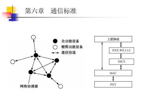
根据设备的功能,ZigBee 网络定义了三种设备:协调器、路由器和终端设备。
协调器和路由器必须是FFD 设备,终端设备可以是FFD 或RFD 设备。
每个ZigBee 网络都必须有且仅有一个协调器,也称为PAN 协调器。
当一个全功能设备启动时,首先通过能量检测等方法确定有无网络存在,有则作为子设备加入,无则自己作为协调器,负责建立并启动网络,包括广播信标帧以提供同步信息、选择合适的射频信道、选择唯一的网络标识符等一系列操作。
路由器在节点设备之间提供中继功能,负责邻居发现、搜寻网络路径、维护路由、存储转发数据,以便在任意两个设备之间建立端到端的传输。
路由器扩展了ZigBee 网络的范围。
终端设备就是网络中的任务执行节点,负责采集、发送和接收数据,在不进行数据收发时进入休眠状态以节省能量。
协调器和路由器也可以负责数据的采集。
ZigBee 网络有信标和非信标两种工作模式。
在信标工作模式下,网络中所有设备都同步工作、同步休眠,以减小能耗。
网络协调器负责以一定的时间间隔广播信标帧,两个信标帧之间有16个时隙,这些时隙分为休眠区和活动区两个部分,数据只能在网络活动区的各时隙内发送。
在非信标模式下,只有终端设备进行周期性休眠,协调器和路由器一直处于工作状态。
ZigBee 网络的拓扑结构有星型、网状和簇树三种,如图6-11所示。
在实际环境中,拓扑结构取决于节点设备的类型和地理环境位置,由协调器负责网络拓扑的形成和变化。
星型拓扑网状拓扑簇树拓扑PAN 协调器全功能设备精简功能设备图6-11 ZigBee 网络的拓扑结构星型拓扑组网简单、成本低、电池使用寿命长,但是网络覆盖范围有限,可靠性不如网状拓扑结构,对充当中心节点的PAN 协调器依赖性较大。
网状拓扑中的每个全功能节点都具有路由功能,彼此可以通信,网络可靠性高、覆盖范围大,但是电池使用寿命短、管理复杂。
一、ZigBee之基本概念物联网的定义是:通过射频识别(RFID)、红外感应器、全球定位系统、激光扫描器等信息传感设备,按约定的协议,把任何物体与互联网相连接,进行信息交换和通信,以实现对物体的智能化识别、定位、跟踪、监控和管理的一种网络。
无线传感网络的定义是:大规模,无线、自组织、多跳、无分区、无基础设施支持的网络.其中的节点是同构的、成本较低、体积较小,大部分节点不移动,被随意撒布在工作区域,要求网络系统有尽可能长的工作时间。
在通信方式上,虽然可以采用有线、无线、红外和光等多种形式,但一般认为短距离的无线低功率通信技术最适合传感器网络使用,为明确起见,一般称无线传感器网络(WSN.Wireless Sensor Network)。
无线传感网络的无线通信技术可以采用ZigBee技术、蓝牙、Wi-Fi和红外等技术。
ZigBee技术是一种短距离、低复杂度、低功耗、低数据速率、低成本的双向无线通信技术或无线网络技术,是一组基于IEEE802.15.4无线标准研制开发的组网、安全和应用软件方面的通信技术。
Zigbee是IEEE 802.15.4协议的代名词。
根据这个协议规定的技术是一种短距离、低功耗的无线通信技术。
这一名称来源于蜜蜂的八字舞,由于蜜蜂(bee)是靠飞翔和“嗡嗡”(zig)地抖动翅膀的“舞蹈”来与同伴传递花粉所在方位信息,也就是说蜜蜂依靠这样的方式构成了群体中的通信网络。
其特点是近距离、低复杂度、自组织、低功耗、低数据速率、低成本。
主要适合用于自动控制和远程控制领域,可以嵌入各种设备。
简而言之,ZigBee就是一种便宜的,低功耗的近距离无线组网通讯技术。
IEEE 802.15.4是一个低速率无线个人局域网(Low Rate Wireless PersonalArea Networks,LR-WPAN)标准。
该标准定义了物理层(PHY)和介质访问控制层(MAC)。
这种低速率无线个人局域网的网络结构简单、成本低廉、具有有限的功率和灵活的吞吐量。

ZigBee 2006协议栈定位系统使用说明书V1.20成都无线龙通讯科技有限公司2007年10月目录0、概述 (31.下载程序至各节点步骤: (111.1初始化物理地址 (111.2正确选择对应程序下载至不同节点 (131.3为每个不同点节分配物理地址。
(132.各节点形成 (132.1网关部分(COORD (132.1.1网关程序下载 (132.1.2分配物理地址 (152.2参考节点部分(ROU (162.3移动节点(也称定位节点部分 (ROU (183.联机调试 (203.1系统硬件连接 (203.2 监控软件设置 (223.3绘制监控区域地图 (223.4参考节点安装 (243.5 移动节点(也称定位节点 (263.6调试 (280、无线定位概述地理定位、方位定位和无线定位这些名词今天被广泛地用来描述确定一个移动台(MS、也称定位节点所在位置的能力。
位置一般包含了和MS有关的坐标,坐标可以是二维或三维的,通常包含了与MS 所在位置的经度和纬度的有关信息。
无线定位技术最初是为了满足远程航海的导航等要求而产生的。
全球定位系统GPS的出现使得无线定位技术产生了质的飞跃,定位精度得到大幅度提高,精度可达10米以内。
国外对于无线定位在移动通信中的应用也有所要求,例如,美国联邦通信委员会(FCC强制要求所有无线业务提供商,在移动用户发出紧急呼叫时,必须向公共安全服务系统提供用户的位置信息和终端号码,以便对用户实施紧急救援工作。
全球三大通信厂商:爱立信、摩托罗拉和诺基亚于2000年10月成立了"位置信息互操作论坛LIF(Location Interoperability Forum",其目标是在全球范围内的无线网络和终端上提供基于位置的服务LBS(Location Based Service。
欧洲电信标准化协会ETSI对GSM系统的无线定位也提出了一系列标准。
GPS已经成为室内环境中一项非常成功的定位技术,而现今GPS与无线网络融合起来形成的LBS热,使得移动定位服务产业作为最具有潜力的移动增值业务而迅速发展。
2005 Microchip Technology Inc.DS00965A_CN 第1页AN965引言ZigBee™是专为低速率传感器和控制网络设计的无线网络协议。
有许多应用可从ZigBee 协议受益,其中可能的一些应用有:建筑自动化网络、住宅安防系统、工业控制网络、远程抄表以及PC 外设。
与其他无线协议相比,ZigBee 无线协议提供了低复杂性、缩减的资源要求,最重要的是它提供了一组标准的规范。
它还提供了三个工作频带,以及一些网络配置和可选的安全功能。
如果您正在寻求现有的控制网络技术(例如RS-422、RS-485)或专有无线协议的替代方案,ZigBee 协议可能是您所需的解决方案。
此应用笔记旨在帮助您在应用中采用ZigBee 协议。
可以使用在应用笔记中提供的Microchip ZigBee 协议栈快速地构建应用。
为了说明该协议栈的用法,本文包含了两个有效的演示应用程序。
可将这两个演示程序作为参考或者根据您的需求经过简单修改来采用它们。
此应用笔记中提供的协议栈函数库实现了一个与物理层无关的应用程序接口。
因此,无需做重大修改就可以轻松地在射频(Radio Frequency ,RF )收发器之间移植应用程序。
在此文档末尾的“常见问题解答”中提供了有关Microchip 协议栈和用法的一些常见问题及其答案。
假设此文档假设您熟悉C 编程语言。
文档中大量使用了有关ZigBee 和IEEE 802.15.4规范的术语。
此文档没有详细讨论ZigBee 规范,只提供了对ZigBee 规范的简要概述。
建议您仔细阅读ZigBee 和IEEE 802.15.4规范。
特性Microchip ZigBee 协议栈设计为随着ZigBee 无线协议规范的发展而发展。
在发布此文档时,该协议栈的 1.0版本具有以下特点(欲知最新特性,请参阅源代码版本日志文件version.log ):• 基于ZigBee 规范的0.8版本• 使用Chipcon CC2420 RF 收发器支持2.4GHz 频带• 支持简化功能设备(Reduced Function Device ,RFD )和协调器• 在协调器节点中实现对邻接表和绑定表的非易失性存储• 支持非时隙的星型网络• 可以在大多数PIC18系列单片机之间进行移植• 协同多任务处理架构• 不依赖于RTOS 和应用• 支持Microchip MPLAB ® C18和Hi-Tech PICC-18™ C 编译器• 易于添加或删除特定模块的模块化设计限制Microchip 协议栈的1.0版本包含以下限制。

zigbee协议栈2010-03-10 15:11zigbee协议栈结构由一些层构成,每个层都有一套特定的服务方法和上一层连接。
数据实体(data entity)提供数据的传输服务,而管理实体(managenmententity)提供所有的服务类型。
每个层的服务实体通过服务接入点(Service AccessPoint.SAP)和上一层相接,每个SAP提供大量服务方法来完成相应的操作。
ZigBee协议栈基于标准的OSI七层模型,但只是在相关的范围来定义一些相应层来完成特定的任务。
IEEE 802.15.4—2003标准定义了下面的两个层:物理层(PHY层)和媒介层(MAC层)。
ZigBee联盟在此基础上建立了网络层(NWK 层)以及应用层(APL层)的框架(framework)。
APL层又包括应用支持子层(Application Support Sub—layer,APS)、ZigBee的设备对象(ZigBee Device 0bjects。
ZD0)以及制造商定义的应用对象。
1物理层(PHY)IEEE802.15.4协议的物理层是协议的最底层,承担着和外界直接作用的任务。
它采用扩频通信的调制方式,控制RF收发器工作,信号传输距离约为50m(室内)或150m(室外)。
IEEE802.15.4.2003有两个PHY层,提供两个独立的频率段:868/915MHz 和2.4GHz。
868/915MHz频段包括欧洲使用的868MHz频段以及美国和澳大利亚使用的915MHz频段,2.4GHz频段世界通用。
2媒体访问控制层(MAC)MAC层遵循IEEE802.15.4协议,负责设备间无线数据链路的建立、维护和结束,确认模式的数据传送和接收,可选时隙,实现低延迟传输,支持各种网络拓扑结构,网络中每个设备为16位地址寻址。
它可完成对无线物理信道的接入过程管理,包括以下几方面:网络协调器(coordinator)产生网络信标、网络中设备与网络信标同步、完成PAN的入网和脱离网络过程、网络安全控制、利用CSMA—CA机制进行信道接入控制、处理和维持GTS(Guaranteed Time Slot)机制、在两个对等的MAC实体间提供可靠的链路连接。
讨论ZigBee协议栈的构成以及内部OSAL的工作机理。
ZigBee协议栈OSAL介绍操作系统抽象层OSAL常用术语:1.资源(Resource):任何任务所占用的实体都叫资源,如变量、数组、结构体2.共享资源(Shared Resource):两个或两个以上任务使用的资源,为防止破坏资源,任务在操作共享资源时是独占状态。
3.任务(Task):即线程,简单的程序的执行过程。
任务设计时将问题尽可能分成多个任务,每个任务独立完成某项功能,同时赋予优先级、CPU寄存器和堆栈空间。
一般一个任务设计为一个无限循环。
4.多任务运行(Muti-task Running):其实同一时刻只有一个任务运行。
5.内核(Kernel):内核负责管理各个任务。
包括:分配CPU时间;任务调度;任务间的通信。
6.互斥(Mutual Exclusion):多任务通信最常用方法是共享数据结构。
保护共享资源常用的方法:关中断;使用测试并置位指令(T&S指令);禁止任务切换;使用信号量;7.消息队列(Message Queue):用于任务间传递消息。
OSAL提供如下功能:任务注册、初始化和启动;任务间的同步、互斥;中断处理;储存器分配和管理;OSAL运行机理:OSAL就是一种支持多任务运行的系统资源分配机制。
OSAL是一种基于事件驱动的轮询式操作系统。
、void osal_start_system(void)是ZigBee协议栈的灵魂,不断的查看事件列表,如果有事件发生就调用相应的事件处理函数。
SYS_EVENT_MSG是一个事件集合,是由协议栈定义的事件,即系统强制事件(Mandatory Events),它的定义为:#define SYS_EVENT_MSG 0x8000;它包含如下事件:AF_INCOMING_MSG_CMD 收到一个新的无线数据ZDO_STATE_CHANGE 网络状态发生变化事件,利用它判断终端加入网络后何时向协调器发送数据包。
《ZigBee协议栈的分析与设计》篇一一、引言随着物联网技术的不断发展,无线通信技术也得到了广泛的应用。
ZigBee作为一种基于IEEE 802.15.4标准的低速无线个人区域网络通讯协议,具有低功耗、低成本、覆盖范围广等优点,被广泛应用于智能家居、工业控制、环境监测等领域。
本文将对ZigBee协议栈进行分析与设计,以便更好地理解和应用ZigBee 协议。
二、ZigBee协议栈概述ZigBee协议栈是一种为基于IEEE 802.15.4标准的无线个人区域网络(WPAN)设计的协议栈。
它包括物理层(PHY)、媒体访问控制层(MAC)以及网络层(NWK)和应用层(APL)。
物理层负责无线信号的发送和接收;媒体访问控制层负责解决无线信道访问冲突问题;网络层负责设备之间的网络连接和路由;应用层则提供了丰富的应用接口,方便用户开发应用。
三、ZigBee协议栈分析1. 物理层分析物理层是ZigBee协议栈的基础,它定义了无线信号的传输方式和参数。
在ZigBee中,物理层支持多种传输速率和频段,可以根据实际需求进行选择。
此外,物理层还负责信号的调制、解调、扩频等操作,以保证无线信号的可靠传输。
2. MAC层分析MAC层负责解决无线信道访问冲突问题,它采用了CSMA-CA(载波监听多路访问/冲突避免)机制。
这种机制可以有效地避免信道冲突,提高无线网络的性能。
此外,MAC层还提供了数据传输服务、信道管理等功能。
3. 网络层分析网络层负责设备之间的网络连接和路由。
它采用了基于IEEE 802.15.4标准的地址分配和管理机制,可以实现设备之间的自动组网和路由选择。
此外,网络层还提供了API接口,方便用户开发应用。
四、ZigBee协议栈设计1. 设计目标ZigBee协议栈的设计目标是在保证无线通信可靠性的前提下,尽可能地降低功耗和成本。
因此,在设计中需要充分考虑设备的功耗、成本、可靠性等因素。
2. 设计原则(1)模块化设计:将协议栈分为不同的模块,每个模块负责不同的功能,方便开发和维护。
CC2430ZDKZigBee Development Kit ProUser ManualRev. 1.2.1Table of contents1INTRODUCTION (3)2ABOUT THIS MANUAL (3)3DEFINITIONS (4)4CC2430ZDK CONTENTS (5)4.1H ARDWARE (5)4.2S OFTWARE (5)4.2.1Chipcon Software (5)4.2.23rd party Software (5)4.3T RAINING (5)4.4S UPPORT (5)5GETTING STARTED (6)5.1P OWERING S MART R F04 (6)5.2P OWERING CC2430DB (7)6HARDWARE DESCRIPTION SMARTRF04EB (9)6.1USB I NTERFACE (9)6.2RS-232 INTERFACE (10)6.3U SER INTERFACE (10)6.4A UDIO INTERFACE (10)6.5SPI INTERFACE SWAP JUMPERS (10)6.6I/O CONNECTORS (11)6.7EM CONNECTORS (12)6.8S IGNAL FLOW (13)6.9CC2430EM (13)7HARDWARE DESCRIPTION CC2430DB (14)7.1USB I NTERFACE (14)7.2U SER INTERFACE (14)7.3EEPROM (14)7.4A CCELEROMETER (14)7.5P OTENTIOMETER (15)7.6L IGHT SENSOR (15)7.7I/O CONNECTORS (15)7.8J UMPER SETTINGS (15)7.8.1P3 Jumpers (16)7.8.2P5 Jumpers (17)7.9S IGNAL FLOW (18)8USING THE CC2430ZDK FOR PROTOTYPING (19)9USING THE CC2430DB FOR PROTOTYPING (19)9.1D EBUGGING USING THE USB INTERFACE (19)9.2D EBUGGING WITH THE CC2430 DEBUG CONNECTOR (19)9.3L OW POWER OPERATION (20)9.4U SING THE CC2430SERIAL PORT TO INTERFACE TO RS232 (22)10SMARTRF04EB PROGRAMMING (24)11USING SMARTRF04EB AS AN IN-CIRCUIT EMULATOR (ICE) (25)12FIRMWARE CC2430DB (27)12.1T HE USB MCU BOOTLOADER (27)13PROGRAMMING THE USB MCU (28)13.1USB MCU SIGNAL NAMES (29)14SCHEMATICS (30)15DOCUMENT HISTORY (30)1 IntroductionThe CC2430 is the first single-chip, IEEE 802.15.4 compliant and ZigBee™ SOC (System On Chip) RF transceiver with integrated microcontroller. It provides a highly integrated, flexible low-cost solution for applications using the world wide unlicensed 2.4 GHz frequency band.The CC2430ZDK is the most powerful tool in the market today for developing complete ZigBee™ applications in the minimum timeframe. The kit includes all required hardware and software to evaluate, demonstrate, prototype and develop various ZigBee™ applications.The CC2430ZDK provides you with Figure 8 Wireless' ZigBee™ Software Development Suite including the industry-leading Z-Stack™, a seat in the 2-day Z-Training and six months email support.The CC2430ZDK is a very flexible kit that can be used to develop everything from simple light switches to advanced nodes with many peripherals. A set of ZigBee™ sample applications is included with the kit to allow users to test performance right out of the box.The hardware is representative of an actual application, and is well suited as a prototyping, evaluation and demonstration platform targeting various ZigBee applications. With this kit a ZigBee Logical device type mapped to the IEEE 802.15.4 Full Function and Reduced Function Devices (FFD and RFD) using the CC2430 can be demonstrated. An FFD can take the role of a ZigBee Coordinator, Router, or End Device depending on the ZigBee logical device type configuration. An RFD can act as ZigBee End Device and cannot serve as a ZigBee Coordinator or ZigBee Router.The CC2430ZDK has the capability to demonstrate ZigBee low power capabilities. TheCC2430ZDK is bundled with the Figure 8 Wireless ZigBee stack for evaluation, demonstration, prototyping and developing purposes of the Z-Stack features. The hardware contains an integrated PCB antenna, the IEEE 802.15.4 compliant RF transceiver CC2430 with necessary support components, joystick, buttons and LED’s that can be used to demonstrate the current ZigBee Home Lightning Profile.This User Manual describes how to use the CC2430 ZigBee Development Kit Pro. The Figure 8 Wireless Z-Stack, tools and documentation will be provided as a distribution package available for download from the Chipcon ZigBee Developer Site after the purchase of this kit. When purchased, customers will be provided with a user name and password to access this site to download the Z-Stack End Customer distribution package.2 About this manualThis manual contains both tutorial and reference information, and covers both the hardware and software components of the development kit. The following components of the kit have its own user manual that can be downloaded from the Chipcon web site:- SmartRF® Studio- Chipcon general packet sniffer- IAR EW8051 C-compiler and C-Spy debugger (From www.IAR.se)3 DefinitionsCC2430ZDK CC2430 ZigBee Development Kit Pro. This development kit SmartRF®04DK A collective term used for all development kits for the SmartRF®04platform, i.e. CC2430ZDKSmartRF®04EB Motherboard for Evaluation Modules. Used for PC interface, emulatorand programming tool as well as user interface.CC2430DB CC2430 ZigBee Development Kit Pro. The board described in thisuser manualCC2430EM CC2430 Evaluation Module, a small plug-in module forSmartRF04EB, should be used as reference design for antenna andRF layoutUSB MCU The Silicon Labs C8051F320 MCU used to provide a USB interfaceon the CC2430ZDKFactory firmware The firmware that is supplied programmed into the USB MCU fromthe factory. This firmware supports SmartRF® Studio operation as wellas a stand-alone PER testerPER Packet Error Rate. Counts the number of lost and/or faulty packetsand displays the ratio: (lost/faulty packets)/number of packets sent SoC System on a Chip. A collective term used to refer to Chipcon ICs withon-chip MCU and RF transceiverICE In Circuit Emulator4 CC2430ZDK contents4.1 Hardware2 x SmartRF04EB Evaluation Boards2 x CC2430EM Evaluation Modules2 x 2.4GHz Antennas5 x CC2430DB Demonstration Boards7 x USB cables10 x AA batteries1 x 10-wire flat cable for using SmartRF04EB as emulator for external target4.2 SoftwareSoftware4.2.1 ChipconZ-Stack™ Industry leading ZigBee™ compliant protocol stackZ-Stack Configurator™Z-Stack Profile Builder™Z-Trace™ debug toolSmartRF® Studio configuration and test toolChipcon Packet Sniffer4.2.2 3rd party SoftwareIAR EW8051 C-compiler with C-SPY debugger CD ROM(60 days evaluation license)4.3 Training2-day Z-Training4.4 Support6 months email supportImportant:Contact local telecommunication authorities before transmitting an RF signal to ensure that there are no local restrictions on the use of the 2.400 –2483.5 MHz ISM band. The CC2420 operates in the 2.4 GHz frequency band. Although this frequency band is usually described as “world-wide”, some countries do not allow unlicensed operation in this band.5 Getting startedThis section describes how to perform the most common tasks associated with the ZigBee Development Kit ProThe hardware for the ZigBee Development Kit Pro is based on the CC2430DK. To get started with the ZigBee Development Kit Pro please follow the Quick Start guide on the Chipcon web page for step-by-step information on how to set up the kit.Make sure to install SmartRF® Studio before connecting the ZigBee Development Kit Pro to a PC. SmartRF® Studio can be downloaded from the Chipcon web pages.SmartRf045.1 PoweringIf several power sources are connected, the ZigBee Development Kit Pro will be powered from the supply that supplies the highest voltage.Figure 1: Power switch settingThe Power Switch S3 must be set according to what power source is used. If 3.3V is applied using the power terminal block, the switch should be set to the left position as shown in Figure 1 above. In all other cases, the switch should be set to the right position for power to be applied to the ZigBee Development Kit Pro. This switch can be used to turn off theSmartRF04EB by switching it to the opposite position of that used to turn it on.Figure 2: Power connectorThe 4-10V input is used for powering the ZigBee Development Kit Pro using the on-board voltage regulator. 0V is the ground connection. The 3.3V terminal is used for powering the ZigBee Development Kit Pro, bypassing the on-board voltage regulator. A voltage between 2.7-3.6V can be used when USB is not active, when using USB the voltage should be limited to 3.0-3.6V.When shipped from the factory, a jumper is placed between I_OUT and I_IN. To measure the current draw of only the EM, remove the jumper and measure the current using an amperemeter.The SmartRF04EB can be powered in several different ways:•DC jack connector with standard DC jack power connectors with a 2.5mm centre pin. The centre pin is used for the positive voltage. A 4-10V DC power supply should be used. The onboard voltage regulator supplies 3.3V to the board.•Laboratory power supply. Ground should be connected to the 0V terminal on the power connector (see Figure 2). A 4-10V supply can be connected to the “4-10V” terminal, or a3.3V supply can be connected to the “3.3V” terminal (the on-board voltage regulators willbe bypassed in this case). If a 3.3V supply is used, the supply selection switch should be set to the “3V” position, otherwise the “4-10V” position should be used. If the “4-10V”position is selected, a voltage regulator supplies the circuitry on the ZigBee Development Kit Pro; otherwise the 3.3V supply is applied directly to the SmartRF04EB.•USB power. If the SmartRF04EB is connected to a USB socket on a PC, it will draw power from the USB bus. The onboard voltage regulator supplies 3.3V to the board. •Battery power. The evaluation board includes a 9V-type battery connector on the bottom side of the PCB. A 9V battery or a battery pack that uses a 9V-type connector can be connected to this battery connector. The onboard voltage regulator supplies 3.3V to the board.Please note that while the SmartRF04 devices have a wide supply range, the components on the ZigBee Development Kit Pro limit the total voltage supply range to 2.7V – 3.6V (3.0V – 3.6V while the USB is active). The ZigBee Development Kit Pro has been designed for a temperature range of –40°C to +85°C (excluding the LCD display). The EM is designed for a temperature range of -40°C to +85°C.CC2430DB5.2 PoweringThe CC2430ZDK can be powered in three different ways:•DC jack connector with standard DC jack power connectors with a 2.5mm centre pin.The centre pin is used for the positive voltage. A 4-10V DC power supply should beused. The onboard voltage regulator supplies 3.3V to the board.•USB power. If the CC2430DB is connected to a USB socket on a PC, it will draw power from the USB bus. The onboard voltage regulator supplies 3.3V to the board.•Battery power. The ZigBee Development Kit Pro includes a battery clip for two AA type batteriesIf several power sources are connected, the CC2430 will be powered from the supply that supplies the highest voltage. The USB MCU is only powered when USB or DC jack power is used.Figure 3: Power switch settingThe Power Switch S3 must be set according to what power source is used. If DC jack or USB power is applied, the switch should be set to the USB position. If the board is powered from batteries, the switch should be set to the BATT position as shown in Figure 3 above. When either DC power or batteries are used to power the board, the switch can be used as an on/off switch.When powering the CC2430DB from batteries, the CC2430 will work down to 1.8V. Please note that when using USB, the voltage range is limited to 3.0V – 3.6V. The CC2430DB has been designed for a temperature range of –40 C to +85 C.6 Hardware description SmartRF04EBFigure 4: CC2430ZDK overviewThe figure above shows the major parts of the SmartRF04. The SmartRF04serves as main platform in the development kit and is designed so that it will support future Chipcon ICs as well.6.1 USB InterfaceThe USB interface is used to interface to a PC to run SmartRF ® Studio and for programming and debugging using the PC debugging tools and programmers. If SmartRF ® Studio connects to the SmartRF04EB and detects an old version of the USB MCU the USB MCU will beupgraded via this interface. The SmartRF04EB can be bus-powered from the USB interface.connector Joystick LEDsI/O connector AI/O connector BVolume controlUSB MCU USB MCUinterface6.2 RS-232The RS-232 can be used by custom applications for communication with other devices. The RS-232 interface utilises a voltage translation device so that the RS-232 port is compatible with bipolar RS-232 levels.Note that this RS-232 level converter contains a charge-pump power supply that generates electric noise.interface6.3 UserThe CC2430ZDK includes a joystick and a push button as user input devices, and four LEDs and a 2x16 character LCD display as user output devices. The display and user interface is controlled by the application example program loaded in the CC2430.The factory firmware uses the joystick, push button and LCD display to implement a menu system used to control the packet error rate handling.interface6.4 AudioThe SmartRF04EB includes a microphone input and headphone output. This interface is not used by Zigbee and IEEE 802.15.4 specific Chipcon devices.The audio output section consists of a volume control, followed by a 4th order Chebyshev filter. This filter serves to attenuate frequencies above 6 kHz, and so converts the PWM signal to an analogue audio signal. A headphone amplifier IC (TPA4411 from Texas Instruments) is used to drive the headphones.Note that the headphone amplifier IC uses switch-mode power supply techniques to generate a negative noise, and this may cause electrical noise. The headphone amplifier can be disabled by driving a pin on the USB MCU low (the same pin is used to disable the RS-232 voltage converter).The audio input section consists of a microphone amplifier that also includes a low-pass anti-aliasing filter.A standard PC-type headset with separate microphone and headphone mini-jacks can be connected directly to the audio interface.6.5 SPI interface swap jumpersDue to a bug in early revisions of CC2430, the MISO and MOSI pins changed directions when switching between SPI slave and master modes. The default settings of the jumpers are SPI master mode, see Figure 5: SPI jumper. To use CC2430 in SPI slave mode, the jumpers must be mounted 90°. SPI slave mode is used by the packet sniffer.Figure 5: SPI jumper6.6 I/OconnectorsThe I/O connectors bring out all the signals from the EM connectors. These connectors are compatible with Agilent logic analyser probes. The connectors allow easy access to I/O signals and to connect prototyping boards.Pin Function1 N/C2 N/C3 P0_0/MIC_IN4 VDD5 VDD6 N/C7 P0_1/BUTTON_PUSH8 N/C9 P0_2/UART_RD10 N/C11 P0_3/UART_TD12 N/C13 P0_4/RTS14 N/C15 P0_5/JOY_PUSH16 N/C17 P0_6/JOY18 N/C19 P0_7/POT20 GNDTable 1: I/O connector A (P10) pin-outPin Function1 N/C2 N/C3 VDD4 P2_0*/LED45 P1_0/LED16 P2_1/DD7 P1_1/PWM_OUTPUT8 P2_0/DC9 P1_2*/LED210 P2_3*/SDA11 P1_3/LED312 P2_4*/SCL13 P1_4/CSn14 N/C15 P1_5/SCLK16 RESET_N17 P1_6/MOSI18 Debug Data Direction(DD_DIR)19 P1_7/MISO20 GNDTable 2: I/O connector B (P11) pin-out, * see chapter 6.9.connectors6.7 EMThe EM connectors are used for plugging the EM to the CC2430ZDK. The connectors P1 and P2 are used as the main interface.The EM includes RF reference design with the Chipcon IC and all required RF circuitry. It is recommended to copy the RF reference design when designing applications with Chipcon devices in order to achieve best RF performance.Note that while it is possible to plug in EM not belonging to the SmartRF®04 product range into the CC2430ZDK the factory firmware and SmartRF® Studio do not support the use of older devices. This means that CC2430ZDK can be used with custom firmware for prototype using the CC2430ZDK together with older Chipcon RF devices.flow6.8 SignalEM connectorFigure 6: Evaluation Board Signal flowThe signal lines from the EM connectors run via 0-ohm resistors to the USB MCU and the various peripherals on the SmartRF04. This allows connecting an EM module to other applications. The USB MCU can be disconnected from the signal pins by removing the 0-ohm resistors. The I/O connectors are located on the “outside” of the 0-ohm resistors, so they are still connected to the EM connectors even if the 0-ohm resistors are removed. Please refer to Table 11 on page 29 for a list of what resistors correspond to which signals.6.9 CC2430EMOn CC2430EM port P2_3 and 2_4 is connected to a 32kHz X-oscillator. The LCD display is therefore internally, on CC2430EM, swapped from P1_2 to P2_3 and P2_0 to P2_4.P2_3P2_4Figure 7: CC2430EM LCD connection7 Hardware description CC2430DBFigure 8: CC2430DB overview7.1 USB InterfaceThe USB interface is used to interface to a PC to run the In-Circuit Emulator in the IAR Embedded Workbench and using SmartRF ® Studio. It is also possible to reprogram the CC2430DB via this interface with the Chipcon programming software, and use the Chipcon packet sniffer. When connected to the USB port the CC2430DB is powered from the USB and no other voltage supplies are required. 7.2 User interfaceThe CC2430DB includes a joystick and a push button as user input devices, and two LEDs as user output devices. 7.3 EEPROMA 32Kbit EEPROM is included for non volatile storage of data that is frequently updated. The EEPROM have 1 Million guaranteed write cycles. 7.4 AccelerometerThe accelerometer can be used measure movements in 2-axis, it can also be used for tilt measurement by measuring the earths gravitation. Accelerometer self test can be initiated by shorting pin 5 and 6 on connector P3. The accelerometer has a 20 ms start-up time after power on. See the Analog Devices ADXL321 datasheet for details about the accelerometer.7.5 PotentiometerThe potentiometer resistance depends on the rotation. Typical value is 10K.sensor7.6 LightA light dependent resistor (LDR) measures light level and gives an analogue signal that is measured by the CC2430 A/D converter. The light sensor resistance ranges from 5KΩ (light) to 20MΩ (dark).connectors7.7 I/OThe I/O connectors bring out all the signals from CC2430. These connectors allow easy access to all CC2430 I/O pins. For prototyping external circuitry can be connected using these connectors.Pin Function1 VDD2 VDD_SW_CONTROLLED13 P0_0/LDR4 RESET_NPUSH5 P0_1/BUTTON6 P1_7/SO/MISO/UART_RD7 P0_2/EE_SDA8 P1_6/SI/MOSI/UART_TD9 P0_3/EE_SCL10 P1_5/SCLK/RTS11 P2_1/DD12 P1_4/CSN/SS/CTS13 P2_2/DCPUSH14 P2_0/JOY15 P0_6/JOY16 P1_2/VDD_SW_CTRL17 P0_7/POT18 P1_1/LED219 P1_0/LED120 GNDTable 3: I/O connector A (P6) pin-outPin Function1 P1_3/GPIO2 DC_JACK_PWR3 P0_4/ACC_X4 VDD5 P0_5/ACC_Y6 GNDTable 4: I/O connector B (P7) pin-out7.8 Jumpersettings1 VDD_SW_CONTROLLED is controlled by the signal named VDD_SW_CTRLFigure 9: CC2430DB Jumper settingsTable 5: Jumper settings summary7.8.1 P3 JumpersThe jumper between pin 1-2 on P3 can be replaced with an ampere meter to measure current consumption of CC2430. The jumper must be mounted for normal operation.The jumper between pin 2-3 can be removed to when performing current measurement to reduce leakage current of the peripheral devices connected to the CC2430. The jumper must be mounted for normal operationThe jumper between pin 5-6 can be mounted to perform accelerometer self test function. By mounting this jumper, a voltage is applied to the accelerometer outputs. See the AnalogHeader Pin DescriptionDefault setting P3 1-2 Replace with ampere meter to measure current consumption of CC2430Mounted P3 3-4 SW controlled power. Can be removed when performing current measurement to reduce leakage currentMountedP3 5-6 Accelerometer self test. Mount to perform accelerometer self test function Not mounted P4 7-9 Manual reset of USB MCUNot mounted P4 9-10 Mount during power on to force USB MCU into boot loaderNot mounted P5 1-2 Connects DD (Debug Data) between USB MCU and CC2430. Should be removed when connecting ICE to “SOC debug connector”Mounted P5 3-4 Connects DC (Debug Clock) between USB MCU and CC2430. Should be removed when connecting ICE to “SOC debug connector”Mounted P5 5-6Connects RESET_N signal between USB MCU and CC2430. Can be removed when performing current measurement to reduce leakage currentMountedDevices ADXL321 datasheet for details about the accelerometer self test. The jumper must be removed for normal operation.Figure 10: Default P3 jumper settings7.8.2 P5JumpersAll jumpers on header P5 must be mounted for normal operation.The jumper between pin 1-2 on P5 connects DD (Debug Data) between USB MCU andCC2430..The jumper between pin 3-4 on P5 connects DC (Debug Clock) between USB MCU andCC2430DB..When the CC2430DB is used with emulator connected to the USB port both the DD and DC jumpers must be mounted. They should only be removed if an external emulator is used. See chapter 9.1 for instructions how to connect external emulator to the CC2430DB.The jumper between pin 5-6 on P5 connects RESET_N signal between USB MCU andCC2430. The jumper can be removed when performing current measurement to reduce leakage current for the circuits connected to the RESET pin. The jumper must be mounted for normal operation.Figure 11: P5 default jumper settingsflow7.9 SignalThe signal lines from the I/O connectors run via 0Ω resistors to the CC2430. and the various peripherals on the ZigBee Development Kit Pro. This way peripheral can be disconnected from the CC2430 signal pins by removing the 0Ω resistors. Please refer to Table 8 for a list of what resistors correspond to which signals.Figure 12: CC2430DB Signal flow8 Using the CC2430ZDK for prototypingSmartRF04EB includes a debug and programming interface. The debug interface is controlled by 2 communication pins. On the SmartRF04EB the interface is controlled by the USB MCU. This allows programming and emulator interface using the USB port. For developing applications, a set of example libraries are include with the SmartRF04EB.Table 11 on page 29 shows what pins on the MCU are used for various peripheral functions. P10 and P11 pin-row connectors can be used to connect the SmartRF04EB to another PCB or prototyping board.Note: The SmartRF04EB may not work with In-Circuit Emulator (ICE), SmartRF® Studio or the examples when the 0-ohm resistors are removed.9 Using the CC2430DB for prototypingThe CC2430DB can be used for prototyping by programming the CC2430 with custom applications. All I/O ports on the CC2430 are available on pin row header at the edge of the board, and the USB interface can be used as In Circuit Emulator (ICE) interface allowing real time in circuit emulation of the CC2430.Code examples and libraries are provided by Chipcon to speed up development with theCC2430DB and CC2430. Table 8 on page 22 shows what pins on the MCU are used for various functions.P6 and P7 pin-row connectors can be used to connect the CC2430DB to other PCB or prototyping boards. See Table 3 on page 15 and Table 4 on page 15 for the pin-out of these connectors.0Ω resistors are included to isolate the CC2430 from the external components on theCC2430DB. By removing these resistors, signals can be accessed on the pin headers.9.1 Debugging using the USB interfaceThe most common way to use the CC2430DB for development is to use the USB interface to control the CC2430 on-chip In-Circuit Emulator. The USB interface supplies power to the board, so there is no need for additional DC power or batteries. The USB interface can also be used to program the CC2430 in circuit using the Chipcon programming software.To use the USB interface, simply connect the USB cable to the board and start the IAR Embedded Workbench software supplied with the kit. Follow the user guide for the IAR tools for instructions how to compile and download the code.9.2 Debugging with the CC2430 debug connectorIt is possible to use the CC2430DB with the Chipcon packet sniffer or other application that requires USB interface for communication with PC and debugging with an emulator simultaneously. In these cases the CC2430 SOC debug connector can be used for connecting the ICE. The SmartRF04EB can be used as emulator interface with a cable from P14 “SOC debug flash” on SmartRF04EB to P8 “SOC debug connector” on CC2430DB. See Figure 13 below. The jumpers between pin 1-2, 3-4 and 4-5 on header P5 must be removed. CC2430DB must be powered from battery, USB or DC jack when debugged fromSmartRF04EB.Figure 13: CC2430 Debug Connectoroperationpower9.3 LowCC2430DB is designed for low power operation when running from batteries. Only theCC2430 is powered in this mode, the USB MCU is not powered. The voltage to the peripheral functions connected to the CC2430 is controlled by an I/O pin P1.2 on the CC2430. Table 6 lists the current consumption for each of the peripherals.To obtain minimum current consumption with the CC2430DB, the P1.2 output must be configured as output.Figure 14: Voltage supply distributionTable 6 below shows the current consumption for all modules and operation modes with 3.3Vsupply voltageActive mode(mA) Power down mode(µA)TypicalMax32KhzSleep CC2430 7,2271µA0.3µAEEPROM 13 0Accelerometer 0,49 0Potentiometer 0,33 0Light sensor 0,001 0.015 0LEDs240 Total 9mA54mA1µATable 6: Current consumption summaryTo accurately measure the current consumption of the C the jumpers listed in Table 7 shouldbe removed.Header Pin Description Low power settingP3 1-2 Replace with ampere meter to measure currentconsumption of CC2430 Mounted, or connect ampere meterP3 3-4 SW controlled power. Can be removed whenperforming current measurement to reduceleakage currentNot mountedP5 5-6 Connects RESET_N signal between USB MCUand CC2430. Can be removed when performingcurrent measurement to reduce leakage currentNot mountedTable 7: Jumper setting for low power measurementsIn order to achieve lowest possible current consumption, the I/O ports of the CC2430 should be configured as listed in Power down state in Table 8 below.2430 pinName Schematic Name DescriptionActivestate2Powerdownstate0Ω ohmresistor 11 P0_0 P0_0/LDRLightdependentresistor analoginputINANALOGOUTLOWR506 12 P0_1 P0_1/BUTTON PUSHPush buttoninterrupt activelowIN PULL-UPIN 13 P0_2 P0_2/EE_SDA EEPROM SDAOUTHIGHOUTLOWR505 14 P0_3 P0_3/EE_SCL EEPROM SCLOUTHIGHOUTLOWR504 15 P0_4 P0_4/ACC_XAccelerometerx-axisINANALOGOUTLOWR507 16 P0_5 P0_5/ACC_YAccelerometery-axisINANALOGOUTLOWR508 17 P0_6 P0_6/JOYJoystickanalog signalINANALOGOUTLOWR416 18 P0_7 P0_7/POTPotentiometeranalog inputINANALOGOUTLOWR4302Active state means that Software controlled VDD is on, this should only be enabledwhen required by an I/O module9 P1_0 P1_0/LED1 Green LED OUTHIGHOUTHIGH8 P1_1 P1_1/LED2 Red LED OUTHIGHOUTHIGH6 P1_2 P1_2/VDD_SW_CTRL Voltage controlfor I/OmodulesOUTHIGHOUTLOW5 P1_3 P1_3/GPIO Free I/O forcontrollingexternal signalOUTLOWOUTLOW4 P1_4 P1_4/CSn/SS/CTS OUTLOWOUTLOWR3053 P1.5 P1_5/SCLK/RTS OUTLOWOUTLOWR3082 P1_6 P1_6/SI/MOSI/UART_TD OUTLOWOUTLOWR3061 P1_7 P1_7/SO/MISO/UART_RD OUTLOWOUTLOWR30748 P2_0 P2_0/Joy_push Joystick pushinterrupt activehighIN IN46 P2_1 P2_1/DD Debug Data IN Jumper P545 P2_2 P2_2/DC Debug Clock IN Jumper P510 RESETRESET_N ResetJumperP5Table 8: Pinout CC2430The joystick output is coded as an analog voltage. This has been done in order to save the number of pins required on the MCU to interface with the joystick. The libraries contain functions to decode the ADC values and indicate in what direction the joystick is moved. The push function of the joystick is connected to a digital input pin.9.4 Using the CC2430serial port to interface to RS232The CC2430serial port is accessible on the header connectors as 3.3V signals. An RS232 driver circuit is required to connect to a RS232 port on a PC. The RS232 port on a SmartRF04EB can be connected to the CC2430DB to allow applications to interface to a PC serial port.Table 9 shows the connection between the CC2430DB and the SmartRF04EB. Both the P8 (10-pin) connector and the P8 (20-pin) connector on the CC2430DB can be used, but only one of them should be connected.To use the serial port on CC2430DBUSART1 must be used on alternative location 2 in the CC2430. Please see the CC2430datasheet for instructions how to select serial port and location. Using the SmartRF04EB will only work if the CC2430DB is powered from a USB or DC jack. The serial port signals will not be accessible if the CC2430DB is powered from batteries.Signal Name Smartrf04EB (P10) CC2430ZDK (P8)”2430 Debug” CC2430ZDK (P6) ”I/O A”RD 9 10 6。
2.ZigBee2.1设备类型(Device Types)在ZigBee网络中存在三种逻辑设备类型:Coordinator(协调器),Router(路由器)和End-Device(终端设备)。
ZigBee网络由一个Coordinator以及多个Router和多个End_Device组成。
上图是一个简单的ZigBee网络示意图。
其中黑色节点为Coordinator,红色节点为Router,白色节点为End-Device。
2.1.1Coordinator(协调器)协调器负责启动整个网络。
它也是网络的第一个设备。
协调器选择一个信道和一个网络ID(也称之为PAN ID,即Personal Area Network ID),随后启动整个网络。
协调器也可以用来协助建立网络中安全层和应用层的绑定(bindings)。
注意,协调器的角色主要涉及网络的启动和配置。
一旦这些都完成后,协调器的工作就像一个路由器(或者消失go away)。
由于ZigBee网络本身的分布特性,因此接下来整个网络的操作就不在依赖协调器是否存在。
2.1.2Router(路由器)路由器的功能主要是:允许其他设备加入网络,多跳路由和协助它自己的由电池供电的儿子终端设备的通讯。
通常,路由器希望是一直处于活动状态,因此它必须使用主电源供电。
但是当使用树群这种网络模式时,允许路由间隔一定的周期操作一次,这样就可以使用电池给其供电。
2.1.3End-Device(终端设备)终端设备没有特定的维持网络结构的责任,它可以睡眠或者唤醒,因此它可以可以是一个电池供电设备。
通常,终端设备对存储空间(特别是RAM的需要)比较小。
注意:在Z-Stack 1.4.1中一个设备的类型通常在编译的时候通过编译选项(ZDO_COORDINATOR 和RTR_NWK)确定。
所有的应用例子都提供独立的项目文件来编译每一种设备类型。
2.2栈配置(Stack Profil e)栈参数的集合需要被配置为一定的值,连同这些值在一起被称之为栈配置。
见过的最浅显易懂的ZigBee协议栈解析ZigBee技术是物联网领域最常用的无线技术之一,如果我们要做基于ZigBee技术的物联网应用,最好对ZigBee协议栈有一个基本的了解。
这篇文章对ZigBee协议栈做一个简单明了的介绍。
概述本文准备介绍的ZigBee协议栈是ZigBee2007,也是目前业界最常用的标准版本,对于ZigBee协议栈的演进历程,可以参加《5分钟了解Zigbee的前世今生》。
ZigBee协议栈可以分为四层:物理层(PHY)、媒体访问控制层(MAC)、网络层(NWK)及应用层(APL)。
如图所示,粉色的部分是由IEEE标准中定义的,浅蓝色部分是由ZigBee联盟规定的,黄色部分是由设备厂商自行定义。
ZigBee协议栈图示在ZigBee协议栈的图示中,我们还可以发现有很多圆角矩形,都带有SAP的字样。
SAP的意思就是服务接入点(Service Access Point)的意思,是协议栈层与层之间的接口,协议栈都是分层结构的,接口就是层与层之间的沟通渠道。
协议栈相邻的上下层之间一般都有两个接口,也就是两个SAP。
名字中带字母D的SAP是数据接口,负责层间数据传输;名字中带字母M的SAP是管理接口,供上层或协议栈的管理平面对该层进行控制,比如进行一些参数配置,或读取状态等。
PHY & MAC & NWKZigBee2007协议栈的物理层及MAC层都是IEEE802.5.14-2003标准中定义的。
PHY层(物理层)规定了所使用的频段,以及所使用的编码、调制、扩频、调频等无线传输技术;有了物理层,就有了一个实现点到点之间的信号发射与接收的基础,没有物理层协议,设备间是根本没有办法通信的,有可能都不在一个频段上。
MAC层的主要作用规定了无线信道的访问控制机制,也就是规定各个设备按照什么规矩轮流使用信道;如果没有MAC层协议,节点一多,大家没有个规矩,就会发生信号冲突,谁都没法正常传输数据了。
目录一RexBee基本使用说明 (1)二组网节点查看及通过无线配置其他节点参数 (10)三网络拓扑图及节点路径查看 (13)四巧用NETWORK软件进行组命令帧 (14)一RexBee基本使用说明拿到模块,如果配合我们的开发板,那使用非常方便,如果没有开发板,那也非常简单,只需连RX,TX,VCC,GND这4根线到你们的MCU,就能跟你们进行串口通信,,外观如下图:1如果是有我们开发板,那么将模块插到我们开发板,接上电源,然后开发板上的LED灯会闪烁,说明模块正常运行,接上串口连接到电脑,然后选择相应COM口即可。
有开发板的话,可以略过2,3,4步骤,直接看第5步。
如果没有我们开发板,那么接着往下看。
2首先要找到每个模块的RX,TX,VCC,GND引脚。
1)增强型插针和标准型插针模块(REX3D&REX3DP)的引脚是兼容的,引脚位置如图:1,2引脚为VCC;27,28引脚为GND;13引脚为RX;16引脚为RX;2)增强型贴片和标准型贴片模块(REX3S&REX3SP)的引脚也是兼容的,引脚位置如图:1,2引脚为VCC;30,31,32引脚为GND;18引脚为RX;19引脚为RX;3)超小型模块(REX3U)引脚图:3找到了这4根引脚后,那么只需将他们跟你们的MCU相连即可。
我们的TX接你们的RX,我们的RX接你们的TX,注意,我们的芯片电压是3.3V,如果你们MCU 是5V的话,需要做转换哦,详见各模块Datasheet。
4按上图连接后,然后配置下串口波特率,你们的MCU就能跟我们的模块进行通信了。
5我们的COO的波特率是115200,8,N,1,ROUTER跟ZED的波特率是9600,8,N,1.配置好波特率后,终于可以与我们模块进行通信了。
首先,打开串口调试助手,选择相应COM口。
首先发送AT+VER查看本身是什么节点类型,在发送AT+GETINFO查看工作在什么信道和PANID下(ZIGBEE设备只有在相同的PANID和信道下才能进行通信)发现PANID跟CH相同,那么就可以进行通信了,比如COO要发送01 02 03 04 05 06 到ROUTER,ROUTER收到数据后给COO回复06 05 04 03 02 01,那么直接在COO端发送01 02 03 04 05 06,然后在ROUTER端发送06 05 04 03 02 01即可。
1.概述1.1解析ZigBee堆栈架构ZigBee堆栈是在IEEE 802.15.4标准基础上建立的,定义了协议的MAC和PHY层。
ZigBee设备应该包括IEEE802.15.4(该标准定义了RF射频以及与相邻设备之间的通信)的PHY和MAC层,以及ZigBee堆栈层:网络层(NWK)、应用层和安全服务提供层。
图1-1给出了这些组件的概况。
1.1.1ZigBee堆栈层每个ZigBee设备都与一个特定模板有关,可能是公共模板或私有模板。
这些模板定义了设备的应用环境、设备类型以及用于设备间通信的簇。
公共模板可以确保不同供应商的设备在相同应用领域中的互操作性。
设备是由模板定义的,并以应用对象(Application Objects)的形式实现(见图1-1)。
每个应用对象通过一个端点连接到ZigBee堆栈的余下部分,它们都是器件中可寻址的组件。
图1-1 zigbe堆栈框架从应用角度看,通信的本质就是端点到端点的连接(例如,一个带开关组件的设备与带一个或多个灯组件的远端设备进行通信,目的是将这些灯点亮)。
端点之间的通信是通过称之为簇的数据结构实现的。
这些簇是应用对象之间共享信息所需的全部属性的容器,在特殊应用中使用的簇在模板中有定义。
图1-1-2就是设备及其接口的一个例子:图1-1-2每个接口都能接收(用于输入)或发送(用于输出)簇格式的数据。
一共有二个特殊的端点,即端点0和端点255。
端点0用于整个ZigBee设备的配置和管理。
应用程序可以通过端点0与ZigBee 堆栈的其它层通信,从而实现对这些层的初始化和配置。
附属在端点0的对象被称为ZigBee设备对象 (ZD0)。
端点255用于向所有端点的广播。
端点241到254是保留端点。
所有端点都使用应用支持子层(APS)提供的服务。
APS通过网络层和安全服务提供层与端点相接,并为数据传送、安全和绑定提供服务,因此能够适配不同但兼容的设备,比如带灯的开关。
Zigbee协议栈中文说明1.概述1.1解析ZigBee堆栈架构ZigBee堆栈是在IEEE 802.15.4标准基础上建立的,定义了协议的MAC和PHY层。
ZigBee设备应该包括IEEE802.15.4(该标准定义了RF射频以及与相邻设备之间的通信)的PHY和MAC层,以及ZigBee堆栈层:网络层(NWK)、应用层和安全服务提供层。
图1-1给出了这些组件的概况。
1.1.1ZigBee堆栈层每个ZigBee设备都与一个特定模板有关,可能是公共模板或私有模板。
这些模板定义了设备的应用环境、设备类型以及用于设备间通信的簇。
公共模板可以确保不同供应商的设备在相同应用领域中的互操作性。
设备是由模板定义的,并以应用对象(Application Objects)的形式实现(见图1-1)。
每个应用对象通过一个端点连接到ZigBee堆栈的余下部分,它们都是器件中可寻址的组件。
图1-1 zigbe堆栈框架从应用角度看,通信的本质就是端点到端点的连接(例如,一个带开关组件的设备与带一个或多个灯组件的远端设备进行通信,目的是将这些灯点亮)。
端点之间的通信是通过称之为簇的数据结构实现的。
这些簇是应用对象之间共享信息所需的全部属性的容器,在特殊应用中使用的簇在模板中有定义。
图1-1-2就是设备及其接口的一个例子:图1-1-2每个接口都能接收(用于输入)或发送(用于输出)簇格式的数据。
一共有二个特殊的端点,即端点0和端点255。
端点0用于整个ZigBee设备的配置和管理。
应用程序可以通过端点0与ZigBee 堆栈的其它层通信,从而实现对这些层的初始化和配置。
附属在端点0的对象被称为ZigBee设备对象 (ZD0)。
端点255用于向所有端点的广播。
端点241到254是保留端点。
所有端点都使用应用支持子层(APS)提供的服务。
APS通过网络层和安全服务提供层与端点相接,并为数据传送、安全和绑定提供服务,因此能够适配不同但兼容的设备,比如带灯的开关。
APS使用网络层(NWK)提供的服务。
NWK负责设备到设备的通信,并负责网络中设备初始化所包含的活动、消息路由和网络发现。
应用层可以通过ZigBee设备对象(ZD0)对网络层参数进行配置和访问。
1.1.2 802.15.4 MAC层IEEE 802.15.4标准为低速率无线个人域网(LR-WPAN)定义了OSI模型开始的两层。
PHY层定义了无线射频应该具备的特征,它支持二种不同的射频信号,分别位于2450MHz波段和868/915MHz 波段。
2450MHz波段射频可以提供250kbps的数据速率和16个不同的信道。
868 /915MHz波段中,868MHz支持1个数据速率为20kbps的信道,915MHz支持10个数据速率为40kbps的信道。
MAC层负责相邻设备间的单跳数据通信。
它负责建立与网络的同步,支持关联和去关联以及MAC 层安全:它能提供二个设备之间的可靠链接。
1.1.3 关于服务接入点ZigBee堆栈的不同层与802.15.4 MAC通过服务接入点(SAP)进行通信。
SAP是某一特定层提供的服务与上层之间的接口。
ZigBee堆栈的大多数层有两个接口:数据实体接口和管理实体接口。
数据实体接口的目标是向上层提供所需的常规数据服务。
管理实体接口的目标是向上层提供访问内部层参数、配置和管理数据的机制。
1.1.4 ZigBee的安全性安全机制由安全服务提供层提供。
然而值得注意的是,系统的整体安全性是在模板级定义的,这意味着模板应该定义某一特定网络中应该实现何种类型的安全。
每一层(MAC、网络或应用层)都能被保护,为了降低存储要求,它们可以分享安全钥匙。
SSP是通过ZD0进行初始化和配置的,要求实现高级加密标准(AES)。
ZigBee规范定义了信任中心的用途。
信任中心是在网络中分配安全钥匙的一种令人信任的设备。
1.1.5 ZigBee堆栈容量和ZigBee设备根据ZigBee堆栈规定的所有功能和支持,我们很容易推测ZigBee堆栈实现需要用到设备中的大量存储器资源。
不过ZigBee规范定义了三种类型的设备,每种都有自己的功能要求:ZigBee协调器是启动和配置网络的一种设备。
协调器可以保持间接寻址用的绑定表格,支持关联,同时还能设计信任中心和执行其它活动。
一个ZigBee网络只允许有一个ZigBee协调器。
ZigBee路由器是一种支持关联的设备,能够将消息转发到其它设备。
ZigBee网格或树型网络可以有多个ZigBee路由器。
ZigBee星型网络不支持ZigBee路由器。
ZigBee端终设备可以执行它的相关功能,并使用ZigBee网络到达其它需要与其通信的设备。
它的存储器容量要求最少。
然而需要特别注意的是,网络的特定架构会戏剧性地影响设备所需的资源。
NWK支持的网络拓扑有星型、树型和网格型。
在这几种网络拓扑中,星型网络对资源的要求最低。
ZigBee堆栈应该可以提供ZigBee规范要求的所有功能,因此制造商的重点工作是开发实际的应用。
为了更加容易实现,如果制造商使用某种公共模板,那么可用大多数现成的配置。
如果没有合适的公共模板,则可以充分利用其它模板已经做过的工作创建自己的模板。
ZigBee协议栈体系包含一系列的层元件,其中有IEEE802.15.4 2003标准中的MAC层和PHY层,当然也包括ZigBee组织设计的NWK层。
每个层的元件有其特定的服务功能。
本说明描述内容涉及ZigBee协议栈的各层元件,但侧重于描述最具实际和理论探讨性的APL应用层和NWK网络层。
图1-1为ZigBee栈结构框图。
2.APL应用层介绍2.1.1应用层简介如图2-1所示,ZigBee应用层由三个部分组成,APS子层、ZDO(包含ZDO管理平台)和制造商定义的应用对象。
图2-1 zigbee协议堆栈分层结构2.1.2应用层框架ZigBee中的应用框架是为驻扎在ZigBee设备中的应用对象提供活动的环境。
最多可以定义240个相对独立的应用程序对象,且任何一个对象的端点编号都是从1到240。
此外还有两个附加的终端节点,为了APSDE-SAP的使用:端点号0固定用于ZDO数据接口;另外一个端点255固定用于所有应用对象广播数据的数据接口功能。
端点241-254保留(留给未来扩展使用)。
2.1.2.1应用Profiles应用profiles是一组统一的消息,消息格式和处理方法,允许开发者建立一个可以共同使用的分布式应用程序,这些应用是利用驻扎在独立设备中的应用实体来实现的。
这些应用profiles允许应用程序发送命令、请求数据和处理命令的请求。
2.1.2.2簇簇标识符可用来区分不同的簇,簇标识符联系着从设备流出和向设备流入的数据。
在特殊的应用profiles范围内,簇标识符是唯一的。
2.1.3 ZigBee设备对象ZigBee设备对象(ZDO),描述了一个基本的功能函数,这个功能在应用对象、设备profile和APS 之间提供了一个接口。
ZDO位于应用框架和应用支持子层之间。
它满足所有在ZigBee协议栈中应用操作的一般需要。
此外ZDO还有以下作用:(1)初始化应用支持子层(APS),网络层(NWK),安全服务规范(SSS)。
(2)从终端应用集合中配置的信息来确定和执行安全管理、发现、网络管理、以及绑定管理。
ZDO描述了应用框架层中应用对象的公用接口以及控制设备和应用对象的网络功能。
在终端节点0, ZDO提供了与协议栈中与低一层连接的接口,如果是数据则通过APSDE-SAP,如果是控制信息则通过APSME-SAP。
ZDO的具体描述在2.5节。
2.1.3.1设备发现设备发现是ZigBee设备为什么能发现其他设备的过程。
这有两种形式的设备发现请求:IEEE地址请求和网络地址请求。
IEEE地址请求是单播到一个特殊的设备且假定网络地址已经知道。
网络地址请求是广播且携带一个已知的IEEE地址作为负载。
2.1.3.2服务发现服务发现是为什么一个已知设备被其他设备发现的能力的过程。
服务发现通过在一个已知设备的每一个端点发送询问或通过使用一个匹配服务(广播或者单播)。
服务发现方便定义和使用各种描述来概述一个设备的能力。
服务发现信息在网络中也许被隐藏,在这种情况下,设备提供的特殊服务便可能不在操作发生的时候到达。
2.2 ZigBee应用支持子层APSAPS提供了这样的接口:在NWK层和APL层之间,从ZDO到供应商的应用对象的通用服务集。
这服务由两个实体实现:APS数据实体(APSDE)和APS管理实体(APSME)。
(1)APSDE提供在同一个网络中的两个或者更多的应用实体之间的数据通信。
通过APSDE服务接入点(APSDE-SAP);(2)APSME提供多种服务给应用对象,这些服务包含安全服务和绑定设备,并维护管理对象的数据库,也就是我们常说的AIB。
通过APSME服务接入点(APSME-SAP)。
2.2.1 范围这一小节描述了应用层部分提供的服务规范和生产商定义的应用对象与ZigBee设备对象之间的接口。
规范定义了允许应用对象传输数据的数据服务和提供绑定机制的管理服务。
另外,它还定义了应用支持子层的帧格式和帧类型。
如图2-2图2-2 zigbee帧格式2.2.2 目的这小节的目的是定义ZigBee应用支持子层的功能。
该功能建立在两个基础之上,一是正确运行ZigBee网络层的驱动功能,二是制造商定义的应用对象所需要的功能。
2.2.3 应用支持子层简介应用支持子层给网络层和应用层通过ZigBee设备对象和制造商定义的应用对象使用的一组服务提供了接口,该接口提供了ZigBee设备对象和制造商定义的应用对象使用的一组服务。
通过两个实体提供这些服务:数据服务和管理服务。
APS数据实体(APSDE)通过与之连接的SAP,即APSDE-SAP 提供数据传输服务。
APS管理实体(APSME)通过与之连接的SAP,即APSME-SAP提供管理服务,并且维护一个管理实体数据库,即APS信息库(NIB)。
2.2.3.1 应用支持子层的数据实体(APSDE)APSDE向网络层提供数据服务,并且为ZDO和应用对象提供服务,完成两个或多个设备之间传输应用层PDU。
这些设备本身必须在同一个网络。
APSDU将提供如下服务:生成应用层的协议数据单元(APDU):APSDE将应用层协议数据单元(PDU)加上适当的协议帧头生成应用子层的协议数据单元(PDU)。
绑定:两个设备服务和需求相匹配的能力。
一旦两个设备绑定了,APSDE将可以把从一个绑定设备接受到的信息传送给另一个设备。
组地址过滤:提供了基于终点组成员的过滤组地址信息的能力。
可靠传输:比从网络层仅仅通过端对端的传输增加了可靠性拒绝重复:提供传送的信息不会被重复接收支持大批量的传输:提供两个设备间顺序传输大批量的数据的能力。