TSH511中文资料
- 格式:pdf
- 大小:1.15 MB
- 文档页数:18
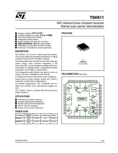
HiFi stereo/mono infrared receiverStereo sub-carrier demodulators Supply voltage: 2.3V to 5.5Vs Carriers frequency range: 0.4 to 11 MHzs Two FM receivers for stereos Integrated audio bufferss Audio outputs: 20 mW into 16 ohmss High sensitivity: 4µV @12dB SINADs Flexibility: access pins for each sections Receiver 2 Standby for mono operation DESCRIPTIONThe TSH511 is a 0.4 to 11 MHz dual FM receiver. This circuit offers the functions needed for a highly sensitive infrared HiFi STEREO receiver. Featuring high input sensitivity and high input dy-namic range, each receiver integrates a RF front-end LNA, an intermediate amplifier with 2 ex-ternal filters, a voltage limiter, a quadrature FM de-modulator, and finally an audio buffer.The integrated audio buffers are able to drive di-rectly a 16 ohms headphone with 20mW.A SQUELCH circuit mutes both audio amplifiers. Access pins to each section makes the TSH511 suited for a wide field of applications.For MONO applications, the STANDBY pin en-ables one receiver only, reducing the supply cur-rent.The TSH511 forms a chipset with the dual trans-mitter TSH512.APPLICATIONSs Infrared HiFi stereo receivers Infrared Multimedia Headsetss Stereo sub-carrier demodulators FM IF receiver systemss Power Line Carrier IntercomsORDER CODE PACKAGEPIN CONNECTION (top view)Part Number TemperatureRange Package Conditionning Marking TSH511CF-40°C to+85°CTQFP44Tray TSH511CTSH511CFT-40°C to+85°C TQFP44 Tape & reelTSH511CTSH511December 20021/18TSH5112/18ABSOLUTE MAXIMUM RATINGSOPERATING CONDITIONSBLOC DIAGRAMSymbol ParameterValue Unit Vcc Supply voltage 1)7V Toper Operating free air temperature range -40 to +85°C Tstg Storage temperature-65 to +150°C Tj Maximum junction temperature150°C Rthjc Thermal resistance junction to case 14°C/W ESDexcept for pin 6HBM: Human Body Model 2)CDM: Charged Device Model 3)MM: Machine Model 4)21.50.2kVESD onlyfor pin 6HBM: Human Body Model CDM: Charged Device Model MM: Machine Model110.1kVLatch-up Class 5)A1. All voltages values, except differential voltage, are with respect to network ground terminal2.ElectroStatic Discharge pulse (ESD pulse) simulating a human body discharge of 100 pF through 1.5k Ω3.Discharge to Ground of a device that has been previously charged.4.ElectroStatic Discharge pulse (ESD pulse) approximating a pulse of a machine or mechanical equipment.5.Corporate ST Microelectronics procedure number 0018695Symbol ParameterValue Unit Vcc Supply voltage 2.3 to 5.5V f audio Audio frequency range 20 to 20,000Hz f carrierCarrier frequency range0.4 to 11MHzTSH511 PIN DESCRIPTIONPin Pin name related to direction1)Pin description1GND--GROUND2AMP-IN2RX2I Intermediate amplifier input3VCC--SUPPLY VOLTAGE4LNA-OUT2RX2O Low Noise Amplifier output5VCC--SUPPLY VOLTAGE6LNA-IN RX1 & RX2I Low Noise Amplifier input7GND--GROUND8LNA-OUT1RX1O Low Noise Amplifier output9VCC--SUPPLY VOLTAGE10AMP-IN1RX1I Intermediate amplifier input11DEC-LNA RX1 & RX2-Decoupling capacitor12AMP-OUT1RX1O Intermediate amplifier input13GND--GROUND14LIM-IN1RX1I Limiter input15DEC-LIM1A RX1-Decoupling capacitor16LIM-OUT1RX1O Limiter output17DEC-LIM1B RX1-Decoupling capacitor18MIX-IN1RX1I Mixer input19VCC--SUPPLY VOLTAGE20MIX-OUT1RX1O Mixer output (demodulated audio signal)21GND--GROUND22BUF-IN1RX1I Audio buffer input23MUTE-IN RX1 & RX2I Noise amplifier input (Squelch circuit)24MUTE-INT RX1 & RX2-Capacitor connection of the noise rectifier25MUTE-OUT RX1 & RX2O Capacitor connection (ramp generator to mute the audio) 26BUF-OUT1RX1O Audio buffer output27GND--GROUND28DEC-OUT RX1 & RX2-Decoupling capacitor of Audio buffers29VCC--SUPPLY VOLTAGE30BUF-OUT2RX2O Audio buffer output31SBY2RX1 & RX2I Standby 232SBY1RX1 & RX2I Standby 133GND--GROUND34BUF-IN2RX2I Audio buffer input35GND--GROUND36MIX-OUT2RX2O Mixer output37VCC--SUPPLY VOLTAGE38MIX-IN2RX2I Mixer input39DEC-LIM2A RX2-Decoupling capacitor40LIM-OUT2RX2O Limiter output41DEC-LIM2B RX2-Decoupling capacitor42LIM-IN2RX2I Limiter input43GND--GROUND44AMP-OUT2RX2O Intermediate amplifier output1.pin direction: I = input pin, O = output pin, - = pin to connect to supply or decoupling capacitors or external components3/18TSH5114/18TYPICAL SCHEMATIC Stereo infrared receiverTSH5115/18INFRARED STEREO HEADPHONE APPLICATIONThe right side of the figure shows the block-diagram of an infrared stereo receiver using the TSH511. The sensitive LNA directly connected to the photodiode does not require an external pre-amplifier. After filter-ing, the amplified signals are limited and demodulated with quadrature demodulators. The two integrated audio buffers directly drive the stereo headphones. The audio power reaches 2x 20mW in two 16Ω loads.The built-in squelch function fades-out the audio when the incoming infrared signal is low. The standby in-puts SBY1 and SBY2 enable only one receiver for the mono applications.buffer2Right Left Audio LNA + ALCLine inputschannelchannel20 mW / 16 Ω20 mW / 16 ΩTSH511MULTIMEDIA APPLICATION: HEADSET SIDEThe TSH511 receives the HiFi stereo sound from the computer through 2.3 and 2.8 MHz stereo infrared carriers. The access pins to the RF amplifiers allow the use of a 1.7 MHz reject filter to cancel the trans-mitted signal of the microphone. The wide supply range (2.3 to 5.5 V) allows battery operation.HiFi stereo2x 20 mW /16to the PCMULTIMEDIA APPLICATION: COMPUTER SIDEIn multimedia application, the TSH511 receives the voice of the user through the 1.7 MHz infrared carrier. The standby pins can disable the unused receiver and audio amplifier to reduce the supply current.6/18TSH5117/18ELECTRICAL CHARACTERISTICSVcc = 2.7V, Tamb = 25°C, faudio = 1 kHz, fcarrier = 2.8 MHz, frequency deviation = +/-75 kHz (unless otherwise specified)SymbolParameterTest conditionMinTypMaxUnitOverall Circuit (refering to typical application schematic, without reject filters) I CC_OXCurrent consumption,RX1 is on, RX2 is on.SBY1 = ’Low’,SBY2 = X (X = don’t care)1518mAI CC_10Current consumptionRX1 is on, RX2 is off RX1 audio buffer is on RX2 audio buffer is on SBY1 = ’High’,SBY2 = ’Low’1113mAI CC_11Current consumptionRX1 is on, RX2 is off RX1 audio buffer is on, RX2 audio buffer is offSBY1 = ’High’,SBY2 = ’High’9.511.5mAMAUS Maximum Usable Average Sensitivitywith audio SINAD=12 dB , audio BW=30 kHz with audio SINAD=26 dB , audio BW=30 kHz 419µV RMSSN OUTOutput audio signal to noise ratioV carrier = 1 mV RMS , with psophometric filter 58dBV i Input limiting voltageoutput S/N reduced by 3dB, in BW = 30kHz output S/N reduced by 3dB, psophometric filter 8060µV RMSTHD Total Harmonic Distortion V carrier = 1 mV RMS , with psophometric filter0.6%Low Noise Amplifier (LNA) Section G LNA LNA voltage gain ZL= 2 k Ω, f carrier = 10 MHz 182228dB BW LNA -3dB LNA BandwidthZL = 2 k Ω20MHz E n_LNA Equivalent input noise voltage Rs = 0 Ω 3.4nV/√Hz I n_LNA Equivalent input noise current Rs = 0 Ω0.6pA/√Hz Z LNA_IN Input impedance definied as R LNA_IN in paralell with C LNA_IN R LNA_IN C LNA_IN302k ΩpF Z LNA_OUT Output impedance 200ΩP 1dB_LNA 1dB compression pointZL= 2 k ΩZL= 2 k Ω, f carrier =10 MHz 12795mV RMS IIP3LNAInput 3rd order interception pointZL= 2 k ΩZL= 2 k Ω, f carrier =10 MHz 3022mV RMSTSH5118/18Amplifier (AMP) Section G AMP Amplifier Voltage Gain ZL=2 k Ω, f carrier =10 MHz 1620dB Z AMP_INInput impedance defined as R AMP_IN in parallel with C AMP_INR AMP_IN C AMP_IN 102k ΩpF Z AMP_OUT Output impedance 350ΩP 1dBAMP 1dB compression point ZL = 2 k ΩZL = 2 k Ω,f carrier =10 MHz 220560380mV RMSBW AMP -3dB AMP BandwidthZL = 2 k Ω11MHzLimitor (LIM) SectionG LIM Voltage gainZL=15k Ω tied to GND 505460dB Z LIM_IN Input impedance defined as R LIM_IN in parallel with C LIM_IN R LIM_IN C LIM_IN152k ΩpF V LIM_OUTOutput VoltageZL = 15 k Ω tied to GND 170mV ppFM Demodulator SectionV DEMOutput voltage+-75 kHz FM deviationtypical application schematicZL = 4 k Ω700800900mV RMSZ DEM_OUT Output impedance 100ΩSquelch SectionATT Audio attenuation on each receiver when audio buffers are muted.RX1 and RX2 audio buff-ers mutedZL = 16 Ω on both audio buffers5565dB Z N_INNoise Amplifier Input impedance2k ΩV N_THComparator thresholdfrom MUTED to UNMUTED state,R MUTE = 22 k Ω,f IN = 100 kHz9mV RMSV N_HYSComparator hysteresisR MUTE = 22 k Ω,f IN = 100 kHz1mV RMSI MUTE_SINK Current sinked on pin 25 to dischargeCMUTE capacitor: ramp generator con-trolling the attenuation from ON to OFF states of audio buffers.Voltage on pin 25 = 1.7V24µAI MUTE_SOU RCE Current sourced on pin 25 to chargeC MUTE capacitor: ramp generator con-trolling the attenuation from OFF to ONstates of audio buffers.Voltage on pin 25 = 1.7V14µASymbolParameter Test condition Min Typ Max UnitTSH5119/18Audio Buffers Z OD-IN Input Impedance 200k ΩBW 1dB -1dB bandwith ZL = 16 Ω35kHz P OUT_ODOutput powerZL= 16ΩV OD_IN = 70mV RMS 1520mWTHD ODDistortion in Line Driver mode Vout = 0.5 V RMS , Z L = 10k Ω0.20.3%THD ODDistortion in Power Amplifier mode with decoupling capacitor CDEC = 1µF/ceramic on pin 28.Pout = 20 mW, ZL = 16Ω0.350.8%V ISOL Crosstalk: isolation between the two Audio BuffersPout = 20 mW, ZL = 16Ω51dBStandby V SBY_L Low level input voltage of Standby inputs (Pins 31 & 32)0.1x V CC V V SBY_H High level input voltage of Standby inputs (Pins 31 & 32)0.9x V ccV T ON Turn-on time from Standby mode to Active mode0.5µs T OFFTurn-off time from Active mode to Standby mode0.5µsSymbol Parameter Test condition Min Typ Max UnitTSH51110/18OVERALL CIRCUITSupply current vs. Supply voltageS/N vs. 2.8 MHz Input LevelPSOPH: Signal on Noise Ratio curve measured with a CCITT standard psophometric bandpass characteristic. It approximates the response of human hearing.Squelch Threshold vs. R MUTE Input ResistorSupply current vs. TemperatureSensitivity vs. Supply VoltageAUDIO BUFFERSOutput THD+N vs. Output Power (RL = 16 Ω)Output THD+N vs. Output Power (RL = 32 Ω)Output THD+N vs. Output Power (RL = 32 Ω) Output THD+N vs. Output Power (RL = 600 Ω)Output THD+N vs. Output Voltage (RL = 10kΩ) Output THD+N vs. Frequency (RL = 16 Ω)Output THD+N vs. Frequency (RL = 600 Ω) Output THD+N vs. Output Voltage (RL = 10kΩ) Output THD+N vs. Frequency (RL = 32 Ω) Output THD+N vs. Frequency (RL = 10 kΩ)Output Power vs. TemperatureGENERAL DESCRIPTIONThe TSH511 is a 0.4 to 11 MHz dual FM analogue receiver. The incoming signal is amplified with a 22 dB Low Noise Amplifier (LNA section). The good noise performance of the LNA allows the photodiode for infrared applications to be connect-ed directly to the TSH511 without any external preamplifier. The access pins for each section and the two standby configurations allow a high versa-tility for many applications: HiFi stereo infrared re-ceiver, mono/stereo subcarrier receiver, power line carrier audio.Figure 1 : TSH511 block diagramThe LNA is common to both receivers but the out-put is split in two: one for each receiver. Each LNA output can be connected to a first optional filter for bandpass or reject filtering.The filtered signal is amplified with an intermedi-ate Amplifier (AMP section) followed by a second filter. The AMP sections have 20 dB typical gain. Finally, the signal is amplified and limited in the Limiter (LIM section). The 60 dB amplifier-limiter LIM provides a constant amplitude signal to the demodulator. It reduces AM parasitics demodula-tion in the FM demodulator.The FM demodulator is a classical quadrature de-tector using an external tank.The demodulated signal can be amplified by the Audio Buffer section after de-emphasis. Each Au-dio Buffer can drive a 16 ohms headphone with 20 mW power.The two standby pins SBY1 & SBY2 allow the sec-ond receiver RX2 to be put into standby for mono operation. In mono, it is possible to use both Audio Buffers or only one depending on the combination on SBY1 & SBY2.To avoid noise at the audio output, a Squelch sec-tion mutes the Audio Buffers when no carrier is re-ceived. The Squelch Section uses the demodulat-ed signal of the first receiver (RX1). This signal is highpass filtered, rectified and compared to a threshold to produce the Mute signal (pin 25). When no carrier is received on RX1, the wideband ’FM noise’ on the demodulator increases and the Mute signal mutes the both Audio Buffers. When the carrier is present, the wideband noise on the demodulator output decreases, enabling the Au-dio Buffers.Figure 2 : Infrared audio frequenciesLNA section: Low Noise AmplifierThe Low Noise Amplifier (LNA) has a typical gain of 22 dB to amplify the incoming RF signal from the photodiode. The LNA is common to both re-ceivers sections RX1 and RX2.Figure 3 : LNA schematicIR frequency applications1.6 MHz AM mono1.7 MHz FM mono2.3 MHz FM right channel2.8 MHz FM left channel or monoThe LNA output is directly connected to LNA-OUT1 and LNA-OUT2 pins in parallel (pin 8 and 4 respectively). As the LNA minimum imped-ance load is 1 kΩ, the load impedance on each pin LNA-OUT1 or LNA-OUT2 must be 2 kΩ minimum. The series 50 Ω resistor and the 100 nF capacitor decouple the LNA supply voltage (pin 5), improv-ing noise performance.AMP and LIM sections: Amplifier and Limitor The first filter output is connected to the intermedi-ate amplifier AMP. The gain of AMP is typically 20 dB. The second filter is connected between the output of AMP and the input of the limitor LIM. The 60 dB limitor LIM provides a constant amplitude signal to the FM demodulator. It reduces the AM parasitic effects into the FM demodulator.Figure 4 : AMP and LIM schematicFM demodulator sectionThe FM demodulator is a classical quadrature de-modulator based on a multiplier. The quadrature is performed with the tank circuit Llo inductor and Clo capacitor. The tank circuit is tuned on the re-ceiving frequency.The Rlo resistor is connected in parallel with Llo and Clo to reduce the Q factor of the tank circuit. It allows to adjustment of the demodulation charac-teristic. For a given transmitting deviation, a lower value of Rlo gives a lower demodulated amplitude and reduces the distortion.The AC amplitude on pin 18 must not exceed 300 mV RMS to prevent clipping by the internal ESD di-odes of the circuit.The low output impedance of the demodulator (MIX-OUT pins) drives the external volume control and the de-emphasis filter.Figure 5 : FM demodulator schematicSQUELCH sectionTo avoid audio ’FM noise’ at the speakers when no carrier is received, the TSH511 has a built-in Squelch circuit. The Squelch detects the wide-band ’FM noise’ on the demodulated output and fades-out the audio of both audio buffers.The audio is filtered from the ’FM noise’ using the high-pass RC filter. The cut-off frequency is typi-cally 100kHz. The squelch level depends on the value of the R MUTE resistor in serie with the input pin of the noise amplifier MUTE-IN (pin 23). The detected noise is integrated with the Cpeak ca-pacitor connected to MUTE-INT pin. The DC volt-age on this pin follows the amplitude of the noise.The comparator and the C MUTE capacitor gener-ate the fade-in and fade-out control ramps for the audio buffers. The Squelch has been designed with particular attention to avoid audio pop-noise.Figure 6 : Squelch schematicThe squelch section is driven by the receiver RX1but controls both audio buffers.Audio Buffer sectionsThe audio signal from a FM demodulator enters into the 6dB/octave low-pass filter for de-empha-sis. 50µs and 75µs are standard de-emphasis val-ues.After the de-emphasis network, the potentiometer controls the volume.The Rail-to-Rail output stage of each Audio Buffer is able to drive 20 mW into 16Ω at 2.3V supply voltage. In this condition, the distortion is typically 0.3% before saturation.The Audio Buffers can also drive the other usual impedances used in audio: 32Ω, 600Ω and 10k Ω(see the corresponding distorsion curves).The high input impedances of the Audio Buffers reduce the coupling capacitors to less than 0.1 µF allowing space and cost saving.Standby sectionDepending on the states of the logic inputs SBY1 and SBY2, RX2 and the Audio Buffer2 can be disabled separately. The TSH511 receiver can adapt to different applications by using SBY1 & SBY2 standby pins:In the standard stereo mode, the configuration is: SBY1 = SBY2 = ’Low’In mono mode with one load(example: a single loadspeaker), RX2 and Audio Buffer 2 are disabled, the configuration is SBY1 = SBY2 = ’High’.In mono mode with a stereo load (example: a stereo headphone), the configuration is SBY1 = ’high’, SBY2 = ’Low’.A pin connected to Vcc is at ’High’ state, and ifconnected to GND is at ’Low’ state.SBY1pin 32SBY2pin 31RX1 &audio buffer1RX2audio buffer 2typical useLow Low ON ON ON stereo Low High High Low ON OFF ON mono on the two outputs HighHighONOFFOFFmono on one out-putAPPLICATION SCHEMATICThe infrared carriers are detected by the photodiode and the signal is directly amplified by the TSH511. Optional reject filters can be added in each channel to improve crosstalk performances. Each receiver has a standard bandpass filter (filters F1 & F3) to select the 2.3 and 2.8 MHz carriers. After the FM demodulators, the potentiometers P1 and P2 control the volume levels. The stereo headphones are directly connected to the integrated audio buffers. The potentiometer P3 allows adjustment of the sensitivity of the Squelch. The Squelch function fade-in and fade-out the audio signal depending on the level of the 2.8 MHz carrier.PACKAGE MECHANICAL DATA44 PINS - PLASTIC PACKAGEDimensions Millimeters InchesMin.Typ.Max.Min.Typ.Max.A 1.600.063A10.050.150.0020.006A2 1.35 1.40 1.450.0530.0550.057B0.300.370.400.0120.0150.016C0.090.200.0040.008D12.000.472D110.000.394D38.000.315e0.800.031E12.000.472E110.000.394E38.000.315L0.450.600.750.0180.0240.030L1 1.000.039K0° (min.), 7° (max.)Information furnished is believed to be accurate and reliable. However, STMicroelectronics assumes no responsibility for the consequences of use of such information nor for any infringement of patents or other rights of third parties which may result from its use. No license is granted by implication or otherwise under any patent or patent rights of STMicroelectronics. Specifications mentioned in this publication are subject to change without notice. This publication supersedes and replaces all information previously supplied. STMicroelectronics products are not authorized for use as critical components in life support devices or systems without express written approval of STMicroelectronics.The ST logo is a registered trademark of STMicroelectronics© 2002 STMicroelectronics - All Rights ReservedSTMicroelectronics GROUP OF COMPANIESAustralia - Brazil - China - Finland - France - Germany - Hong Kong - India - Italy - Japan - Malaysia - Malta - MoroccoSingapore - Spain - Sweden - Switzerland - United Kingdom。