OB3393SCPA规格书 Datasheet
- 格式:pdf
- 大小:704.95 KB
- 文档页数:6
ob6683cgpa规格书英文回答:OB6683CGPA Specification.Introduction:The OB6683CGPA specification outlines the requirements and standards for the OB6683CGPA product. Thisspecification aims to provide a detailed description of the product's features, functionality, and performance expectations. In this response, I will discuss the key aspects of the OB6683CGPA specification and provide examples to illustrate its application.Product Features:The OB6683CGPA is a versatile and high-performance device that offers a range of features to meet the needs of users. It is equipped with advanced technology andinnovative design elements. Some of its notable features include:1. High-resolution display: The OB6683CGPA boasts a vibrant and sharp display, allowing users to enjoy crystal-clear visuals and an immersive viewing experience.2. Powerful processor: With a state-of-the-art processor, the OB6683CGPA delivers lightning-fast performance, enabling seamless multitasking and smooth operation of resource-intensive applications.3. Extensive storage capacity: The OB6683CGPA offers ample storage space, allowing users to store a large amount of data, including photos, videos, and documents, without worrying about running out of space.4. Advanced camera system: The OB6683CGPA is equipped with a high-quality camera system, enabling users to capture stunning photos and videos with exceptional clarity and detail.Performance Expectations:The OB6683CGPA is designed to deliver exceptional performance across various tasks and applications. Its powerful hardware and optimized software ensure smooth and efficient operation. Some performance expectations for the OB6683CGPA include:1. Fast and responsive user interface: The OB6683CGPA provides a seamless user experience with its quick and responsive interface. Users can navigate through menus, open applications, and perform tasks without any lag or delay.2. Smooth gaming experience: The OB6683CGPA is capable of handling graphically demanding games with ease. Users can enjoy a smooth and immersive gaming experience without experiencing any frame drops or stuttering.3. Efficient multitasking: The OB6683CGPA allows users to run multiple applications simultaneously without compromising performance. Users can switch between appsseamlessly and enjoy a seamless multitasking experience.4. Long battery life: The OB6683CGPA is equipped with a high-capacity battery that provides extended usage time. Users can enjoy using the device for extended periodswithout worrying about frequent recharging.中文回答:OB6683CGPA规格书。
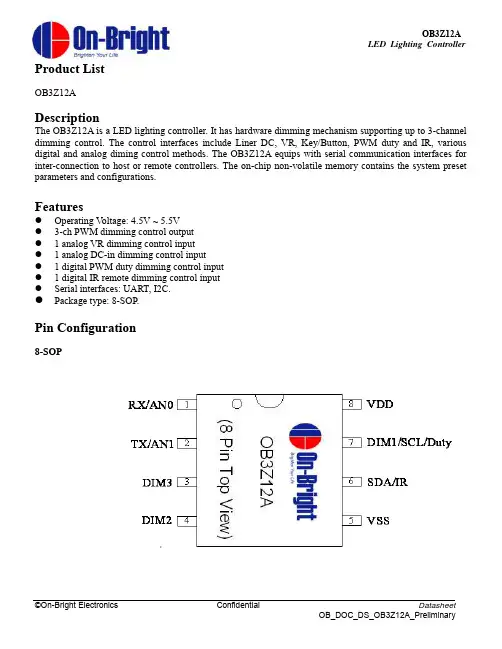
Product ListOB3Z12ADescriptionThe OB3Z12A is a LED lighting controller. It has hardware dimming mechanism supporting up to 3-channel dimming control. The control interfaces include Liner DC, VR, Key/Button, PWM duty and IR, various digital and analog diming control methods. The OB3Z12A equips with serial communication interfaces for inter-connection to host or remote controllers. The on-chip non-volatile memory contains the system preset parameters and configurations.Features●Operating V oltage: 4.5V ~ 5.5V●3-ch PWM dimming control output● 1 analog VR dimming control input● 1 analog DC-in dimming control input● 1 digital PWM duty dimming control input● 1 digital IR remote dimming control input●Serial interfaces: UART, I2C.●Package type: 8-SOP.Pin Configuration8-SOPPin DescriptionPin Symbol I/O Description1 RX/AN0 I VR, analog diming control input. Serial Receiver Input2 TX/AN1 I/O Liner analog diming control input. Serial Transmitter Output3 DIM3 O PWM dimming output ch-34 DIM2 O PWM dimming output ch-25 VSS I Power supply6 SDA/IR I/O I2C Data. IR input7 DIM1/SCL/Duty I/O I2C Clock. PWM dimming output ch-1. Duty dimming control input8 VDD I Power SupplyOperating ConditionsSymbol Description Min. Typ. Max. Unit. RemarksTA Operating temperature -40 25 85 ℃Ambient temperature under bias VDD Supply voltage 4.5 5.5 VDC CharacteristicsT A = -40℃ to 85℃, V dd= 5.0VSymbol Parameter Valid Min Max Units ConditionsVIL1Input Low-voltage DIMx,SDA,SCL,Tx,Rx-0.5 0.8 V Vdd=5VVIH1Input High-voltage DIMx,SDA,SCL,Tx,Rx2.0 V CC + 0.5 VVOL Output Low-voltage DIMx,SDA,SCL,Tx,Rx0.4 V IOL=4.9mAVOH1Output High-voltageusing Strong Pull-upDIMx,SDA,SCL,Tx,Rx90% V CC V IOH= -4.6mA2.4 V IOH= -14mAVOH2Output High-voltageusing Weak Pull-upDIMx,SDA,SCL,Tx,Rx2.4 V IOH= -250uAIIL Logic 0 Input Current DIMx,SDA,SCL,Tx,Rx-75 uA Vin= 0.45VITL Logical TransitionCurrentDIMx,SDA,SCL,Tx,Rx-650 uA Vin= 2.0VILI Input Leakage Current DIMx,SDA,SCL,Tx,Rx±10 uA 0.45V<Vin<VccICC Power Supply Current VDD 5 mA Vdd =5V 25 ℃。
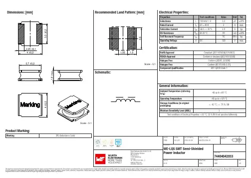
Dimensions: [mm]Scale - 5:1Product Marking:Marking3R3 (Inductance Code)7440404203374404042033BC74404042033T e m p e r a t u r eT pT L74404042033Cautions and Warnings:The following conditions apply to all goods within the product series of WE-LQS of Würth Elektronik eiSos GmbH & Co. KG:General:•This electronic component is designed and manufactured for use in general electronic equipment.•Würth Elektronik must be asked for written approval (following the PPAP procedure) before incorporating the components into any equipment in fields such as military, aerospace, aviation, nuclear control, submarine, transportation (automotive control, train control, ship control), transportation signal, disaster prevention, medical, public information network etc. where higher safety and reliability are especially required and/or if there is the possibility of direct damage or human injury.•Electronic components that will be used in safety-critical or high-reliability applications, should be pre-evaluated by the customer. •The component is designed and manufactured to be used within the datasheet specified values. If the usage and operation conditions specified in the datasheet are not met, the wire insulation may be damaged or dissolved.•Do not drop or impact the components, the component may be damaged.•Würth Elektronik products are qualified according to international standards, which are listed in each product reliability report. Würth Elektronik does not warrant any customer qualified product characteristics beyond Würth Elektroniks’ specifications, for its validity and sustainability over time.•The responsibility for the applicability of the customer specific products and use in a particular customer design is always within the authority of the customer. All technical specifications for standard products also apply to customer specific products.Product specific:Soldering:•The solder profile must comply with the technical product specifications. All other profiles will void the warranty.•All other soldering methods are at the customers’ own risk.•Strong forces which may affect the coplanarity of the components’ electrical connection with the PCB (i.e. pins), can damage the part, resulting in avoid of the warranty.Cleaning and Washing:•Washing agents used during the production to clean the customer application might damage or change the characteristics of the wire insulation, marking or plating. Washing agents may have a negative effect on the long-term functionality of the product.•Using a brush during the cleaning process may break the wire due to its small diameter. Therefore, we do not recommend using a brush during the PCB cleaning process.Potting:•If the product is potted in the customer application, the potting material may shrink or expand during and after hardening. Shrinking could lead to an incomplete seal, allowing contaminants into the core. Expansion could damage the components. We recommend a manual inspection after potting to avoid these effects.Storage Conditions:• A storage of Würth Elektronik products for longer than 12 months is not recommended. Within other effects, the terminals may suffer degradation, resulting in bad solderability. Therefore, all products shall be used within the period of 12 months based on the day of shipment.•Do not expose the components to direct sunlight.•The storage conditions in the original packaging are defined according to DIN EN 61760-2.•The storage conditions stated in the original packaging apply to the storage time and not to the transportation time of the components. Packaging:•The packaging specifications apply only to purchase orders comprising whole packaging units. If the ordered quantity exceeds or is lower than the specified packaging unit, packaging in accordance with the packaging specifications cannot be ensured. Handling:•Violation of the technical product specifications such as exceeding the nominal rated current will void the warranty.•Applying currents with audio-frequency signals may result in audible noise due to the magnetostrictive material properties.•The temperature rise of the component must be taken into consideration. The operating temperature is comprised of ambient temperature and temperature rise of the component.The operating temperature of the component shall not exceed the maximum temperature specified.These cautions and warnings comply with the state of the scientific and technical knowledge and are believed to be accurate and reliable.However, no responsibility is assumed for inaccuracies or incompleteness.Würth Elektronik eiSos GmbH & Co. KGEMC & Inductive SolutionsMax-Eyth-Str. 174638 WaldenburgGermanyCHECKED REVISION DATE (YYYY-MM-DD)GENERAL TOLERANCE PROJECTIONMETHODChriB001.0072023-02-28DIN ISO 2768-1mDESCRIPTIONWE-LQS SMT Semi-ShieldedPower Inductor ORDER CODE74404042033SIZE/TYPE BUSINESS UNIT STATUS PAGEImportant NotesThe following conditions apply to all goods within the product range of Würth Elektronik eiSos GmbH & Co. KG:1. General Customer ResponsibilitySome goods within the product range of Würth Elektronik eiSos GmbH & Co. KG contain statements regarding general suitability for certain application areas. These statements about suitability are based on our knowledge and experience of typical requirements concerning the areas, serve as general guidance and cannot be estimated as binding statements about the suitability for a customer application. The responsibility for the applicability and use in a particular customer design is always solely within the authority of the customer. Due to this fact it is up to the customer to evaluate, where appropriate to investigate and decide whether the device with the specific product characteristics described in the product specification is valid and suitable for the respective customer application or not.2. Customer Responsibility related to Specific, in particular Safety-Relevant ApplicationsIt has to be clearly pointed out that the possibility of a malfunction of electronic components or failure before the end of the usual lifetime cannot be completely eliminated in the current state of the art, even if the products are operated within the range of the specifications.In certain customer applications requiring a very high level of safety and especially in customer applications in which the malfunction or failure of an electronic component could endanger human life or health it must be ensured by most advanced technological aid of suitable design of the customer application that no injury or damage is caused to third parties in the event of malfunction or failure of an electronic component. Therefore, customer is cautioned to verify that data sheets are current before placing orders. The current data sheets can be downloaded at .3. Best Care and AttentionAny product-specific notes, cautions and warnings must be strictly observed. Any disregard will result in the loss of warranty.4. Customer Support for Product SpecificationsSome products within the product range may contain substances which are subject to restrictions in certain jurisdictions in order to serve specific technical requirements. Necessary information is available on request. In this case the field sales engineer or the internal sales person in charge should be contacted who will be happy to support in this matter.5. Product R&DDue to constant product improvement product specifications may change from time to time. As a standard reporting procedure of the Product Change Notification (PCN) according to the JEDEC-Standard inform about minor and major changes. In case of further queries regarding the PCN, the field sales engineer or the internal sales person in charge should be contacted. The basic responsibility of the customer as per Section 1 and 2 remains unaffected.6. Product Life CycleDue to technical progress and economical evaluation we also reserve the right to discontinue production and delivery of products. As a standard reporting procedure of the Product Termination Notification (PTN) according to the JEDEC-Standard we will inform at an early stage about inevitable product discontinuance. According to this we cannot guarantee that all products within our product range will always be available. Therefore it needs to be verified with the field sales engineer or the internal sales person in charge about the current product availability expectancy before or when the product for application design-in disposal is considered. The approach named above does not apply in the case of individual agreements deviating from the foregoing for customer-specific products.7. Property RightsAll the rights for contractual products produced by Würth Elektronik eiSos GmbH & Co. KG on the basis of ideas, development contracts as well as models or templates that are subject to copyright, patent or commercial protection supplied to the customer will remain with Würth Elektronik eiSos GmbH & Co. KG. Würth Elektronik eiSos GmbH & Co. KG does not warrant or represent that any license, either expressed or implied, is granted under any patent right, copyright, mask work right, or other intellectual property right relating to any combination, application, or process in which Würth Elektronik eiSos GmbH & Co. KG components or services are used.8. General Terms and ConditionsUnless otherwise agreed in individual contracts, all orders are subject to the current version of the “General Terms and Conditions of Würth Elektronik eiSos Group”, last version available at .Würth Elektronik eiSos GmbH & Co. KGEMC & Inductive SolutionsMax-Eyth-Str. 174638 WaldenburgGermanyCHECKED REVISION DATE (YYYY-MM-DD)GENERAL TOLERANCE PROJECTIONMETHODChriB001.0072023-02-28DIN ISO 2768-1mDESCRIPTIONWE-LQS SMT Semi-ShieldedPower Inductor ORDER CODE74404042033SIZE/TYPE BUSINESS UNIT STATUS PAGE。
12REFERENCEDESIGNATOR QUANTITY PART NUMBER DESCRIPTION VENDOR TELEPHONE ADJ10Optional ResistorC110603ZG105ZAT1A1µF 10V Y5V Chip Capacitor AVX(843) 946-0362 C210402ZG104ZAT1A0.1µF 10V Y5V Chip Capacitor AVX(843) 946-0362 C31LMK325BJ106MN10µF 10V X7R Chip Capacitor Taiyo-Yuden(408) 573-4150 E1 to E442308-2Pad Turret Mill-Max(516) 922-6000 JP10Optional JumperJP216351-12G1Connector, SMT2X6, 0.39" Gap Comm-Con(626) 301-4200 Shunts for2CTAIJ1MM-G Shunts for 0.39" Gap Comm-Con(626) 301-4200 JP1 and JP2R11CR05-2613FM261k 1/16W 1% Chip Resistor AAC(800) 508-1521 R21CR05-3653FM365k 1/16W 1% Chip Resistor AAC(800) 508-1521 R31CR05-4223FM422k 1/16W 1% Chip Resistor AAC(800) 508-1521 R41CR05-7683FM768k 1/16W 1% Chip Resistor AAC(714) 255-9186 R51CR05-2493FM249k 1/16W 1% Chip Resistor AAC(714) 255-9186 U11LT1762EMS8 or8-Lead MSOP IC Version -A LTC(408) 432-1900 LT1962EMS88-Lead MSOP IC Version -BPARTS LISTOPERATIOUHOOK-UPSolid turret terminals are provided for easy connection to supplies and test equipment. Connect a 0V to 20V, 0.5A power supply across the IN and GND terminals and the load across the OUT and GND terminals. The SHDN pin can be disconnected from IN via JP1 to allow for separate shutdown control via a secondary control line. JP2 can be used to select any of a number of common fixed output voltages, or used in conjunction with ADJ1 to create a custom output voltage using the formula:ADJ1 = (V OUT – 1.22V)/4.93µAOUTPUT CAPACITOR SELECTIONThe output capacitor C3 is a 10µF X7R ceramic chip capacitor. Should a different output capacitor be desired, care must be exercised with the selection. Many ceramic capacitor dielectrics exhibit strong temperature and voltage characteristics that reduce their effective capaci-tance to as low as 10% to 20% of nominal over the full range. For further information, see Linear Technology Application Note 83, “Performance Verification of Low Noise, Low Dropout Regulators,” Appendix␣B, “Capaci-tor Selection Considerations,” reprinted below.CAPACITOR SELECTION CONSIDERATIONSBypass Capacitance and Low Noise Performance Adding a capacitor between the regulator’s V OUT and BYP pins lowers output noise. A good quality, low leakage capacitor is recommended. This capacitor bypasses the regulator’s reference, providing a low frequency noise pole. A 0.01µF capacitor lowers the output voltage noise to 20µV RMS. Using a bypass capacitor also improves transient response. With no bypassing and a 10µF output capacitor, a 10mA to 500mA load step settles within 1% of final value in under 100µs. With a 0.01µF bypass capacitor, the output settles within 1% for the same load step in under 10µs; total output deviation is inside 2.5%. Regulator start-up time is inversely proportional to bypass capacitor size, slowing to 15ms with a 0.01µF bypass capacitor and 10µF at the output.34567Information furnished by Linear Technology Corporation is believed to be accurate and reliable.However, no responsibility is assumed for its use. Linear Technology Corporation makes no represen-tation that the interconnection of its circuits as described herein will not infringe on existing patent rights.8dc339 LT/TP 0301 500 • PRINTED IN USA© LINEAR TECHNOLOGY CORPORA TION 2001Linear Technology Corporation1630 McCarthy Blvd., Milpitas, CA 95035-7417(408) 432-1900 q FAX: (408) 434-0507 q 。
Product ListOB3Z12ADescriptionThe OB3Z12A is a LED lighting controller. It has hardware dimming mechanism supporting up to 3-channel dimming control. The control interfaces include Liner DC, VR, Key/Button, PWM duty and IR, various digital and analog diming control methods. The OB3Z12A equips with serial communication interfaces for inter-connection to host or remote controllers. The on-chip non-volatile memory contains the system preset parameters and configurations.Features●Operating V oltage: 4.5V ~ 5.5V●3-ch PWM dimming control output● 1 analog VR dimming control input● 1 analog DC-in dimming control input● 1 digital PWM duty dimming control input● 1 digital IR remote dimming control input●Serial interfaces: UART, I2C.●Package type: 8-SOP.Pin Configuration8-SOPPin DescriptionPin Symbol I/O Description1 RX/AN0 I VR, analog diming control input. Serial Receiver Input2 TX/AN1 I/O Liner analog diming control input. Serial Transmitter Output3 DIM3 O PWM dimming output ch-34 DIM2 O PWM dimming output ch-25 VSS I Power supply6 SDA/IR I/O I2C Data. IR input7 DIM1/SCL/Duty I/O I2C Clock. PWM dimming output ch-1. Duty dimming control input8 VDD I Power SupplyOperating ConditionsSymbol Description Min. Typ. Max. Unit. RemarksTA Operating temperature -40 25 85 ℃Ambient temperature under bias VDD Supply voltage 4.5 5.5 VDC CharacteristicsT A = -40℃ to 85℃, V dd= 5.0VSymbol Parameter Valid Min Max Units ConditionsVIL1Input Low-voltage DIMx,SDA,SCL,Tx,Rx-0.5 0.8 V Vdd=5VVIH1Input High-voltage DIMx,SDA,SCL,Tx,Rx2.0 V CC + 0.5 VVOL Output Low-voltage DIMx,SDA,SCL,Tx,Rx0.4 V IOL=4.9mAVOH1Output High-voltageusing Strong Pull-upDIMx,SDA,SCL,Tx,Rx90% V CC V IOH= -4.6mA2.4 V IOH= -14mAVOH2Output High-voltageusing Weak Pull-upDIMx,SDA,SCL,Tx,Rx2.4 V IOH= -250uAIIL Logic 0 Input Current DIMx,SDA,SCL,Tx,Rx-75 uA Vin= 0.45VITL Logical TransitionCurrentDIMx,SDA,SCL,Tx,Rx-650 uA Vin= 2.0VILI Input Leakage Current DIMx,SDA,SCL,Tx,Rx±10 uA 0.45V<Vin<VccICC Power Supply Current VDD 5 mA Vdd =5V 25 ℃。
FORM-70-016-01LED TV CONTROL BOARD SPECIFICATIONMODEL : CV3393BL-G-20Approved by CultraviewApproved by CustomerAUTHOR : WP .WU Comments :CHECKED BY : CHECKED BY :APPROVED BY :APPROVED BY:DATE:2015.06.26DATE:Company’s seal:Please return us one original approved by you with your signatures. 客户承认签章后敬请寄回正本一份C UL T RA V I EWITEM1. CHANGE THE LIST OF UPGRADES (2)2. GENERAL DESCRIPTION (3)3. FEATURES (4)4. PRESET MODE FOR USB (5)5. ENVIRONMENTAL CONDITION (7)6. SUBSTITUTABLE PRIMARY MATERIALS (8)7. PICTURE (10)8. INTERFACE DEFINITION (11)9. CONFIGURATION (13)10. APPLICATION REQUIREMENT (14)11. EXCURSUS (15)1. CHANGE THE LIST OF UPGRADESVersion Description Page redactionChecked DateV1.0 First Release ALL WP .WUJun.26, 2015C UL T RA V I EW2. GENERAL DESCRIPTIONThis product is digital & analogue TV board, can receive the NTSC analogue television and the ATSC digital television. Apply to the North American ATSC high-definition TV market.TV supports ATSC (meet the performance requirements of A74), NTSC, ClearQAM (meet the performance requirements of ITU-J83).Supports USB 2.0 Multimedia Player;supports audio and video play; supportspicture browse.Supports USB update.Analogue and digital HD port input signal largest support 1080PThe largest support various TFT-LCD 1920x1080 resolutions module. HDMI 1.3/1.4 Compliant; HDCP 1.2 Compliant. Supports MHL; Supports ARC.3-D video decoding and Chroma separation3-D motion adaptive video de-interlacers with edge-oriented adaptive algorithmfor smooth low-angle edges 3-D video noise reductionSupports Closed Caption (analog CC 608/ analog CC 708/digital CC 608/ digitalCC 708),V-chip and SCTE.Supports BTSC/A2/EIA-J demodulationSupports digital audio format decoding:MPEG-1,MPEG2-2(Layer I/II),DolbyDigital(AC-3) Automatic 3:2 pull-down & 2:2 pull-down detection and recoveryMStar 5rd Generation Advanced Color Engine (MStarACE-5) automatic pictureenhancementReliable EMC and ESD handleC UL T RA V I EW3. FEATURESPANELType TFT-LCDResolution Max. 1920X1080 Interface Single/ Double LVDS ATVInput Impedance 75Ω Video System NTSCSound SystemM, J, 4.43.BTSC/A2DTVInput Impedance 75ΩBandwidth 6MHz Modulation ATSC:8VSB QAM:64QAM, 256QAM Video System MPEG 2 MP@HL Sound System MPEG 1/ layer 1/AC-3 PCSync H: 30-75KHz V: 56-75Hz Video Level 0.7Vp-p@75ohm MODE Max 1920X1080@60Hz AVColor system PAL/NTSC/SECAM Video Level 1Vp-p@75ohm Audio Level 500mV rmsYPbPrVideo LevelY:1Vp-p@75ohm,PbPr:0.7Vp-p@75ohm Audio Level 500mVrmsFormat480i, 480p, 576i, 576p, 720p, 1080i, 1080pHDMIVideo Level Standard TMDSFormat480i, 480p, 576i, 576p, 720p, 1080i, 1080pKeyboardPower/Menu/Source/ Up/ Down/ Left/ RightOSD Language English/ French/ Spanish Audio Amplifier 2 X3W @ 4ohm THD<10% Power input DC +12VStandby< 0.3W(Main Board Only)C UL T RA V I EW4. PRESET MODE FOR USBUSB FORMAT MODEMediaFile Exit. Codec RemarkVideoAudio .aviXvid,MPEG-2,MPEG-4,H.264,(Divx Need license) MP3 WMA AAC MP2 PCM(AC3 Need license) (DTS Need license) The Max Resolution And FrameRate:1080p@30fps Max Data Rate: 20 Mbps.mp4 MPEG-2,MPEG-4,H.264(Divx Need license) .mpgMPEG-1,MPEG-2 .mkv / .mov MPEG-1/2/4,H.264, (Divx Need license) .datMPEG-1MP2(AC3 Need license) (DTS Need license)The MaxResolution:352×288 Max Data Rate: 20 Mbps .vob MPEG-2The MaxResolution:720×576 Max Data Rate: 20 Mbps .rm/ .rmvbRV8,RV9, RV10COOKThe Max Resolution And FrameRate:1080p@30fpsMax Data Rate: 10 MbpsPHOTO .jpgProgressive JPEG Max Resolution: 1024×768 .jpegBaseline JPEGMax Resolution: 15360×8640 .bmg---- Max Resolution: 9600×6400 Pixel Depth:1/4/8/16/24/32 bpp.png Non-Interlaced Max Resolution: 9600×6400 InterlacedMax Resolution: 1200×800MUSIC.mp3--- MP3Sample Rate: 32K~48KHzBit Rate: 32K~320Kbps Channel: Mono/Stereo.wma --- WMA.m4a / .aac---AACSample Rate: 8K~48KHz Bit Rate: 24K~384KbpsC UL T RA V I EWChannel: Mono/StereoTEXT .txt ANSI/UNICODE GB/UTF8 File Size:Max 1MBNote :1)This product includes the following optional patented technologies : Dolby, DTS, DIVX, SRS , etc. If you need to use these patented, please provide the patent license to us, so that the product can meet your requirements . (此产品包括如下可选的专利技术:DOLBY 、DTS 、DIVX 、SRS 等,如您需要开通这些功能,请提前提供相关专利许可给到我司,以便产品能满足您的要求。
The MAX338/MAX339 are monolithic, CMOS analog multiplexers (muxes). The 8-channel MAX338 is designed to connect one of eight inputs to a common output by control of a 3-bit binary address. The dual, 4-channel MAX339 is designed to connect one of four inputs to a common output by control of a 2-bit binary address. Both devices can be used as either a mux or a demux. On-resistance is 400Ωmax, and the devices conduct current equally well in both directions.These muxes feature extremely low off leakages (less than 20pA at +25°C), and extremely low on-channel leakages (less than 50pA at +25°C). The new design offers guaranteed low charge injection (1.5pC typ) and electrostatic discharge (ESD) protection greater than 2000V, per method 3015.7. These improved muxes are pin-compatible upgrades for the industry-standard DG508A and DG509A. For similar Maxim devices with lower leakage and charge injection but higher on-resis-tance, see the MAX328 and MAX329.The MAX338/MAX339 operate from a single +4.5V to +30V supply or from dual supplies of ±4.5V to ±20V.All control inputs (whether address or enable) are TTL compatible (+0.8V to +2.4V) over the full specified tem-perature range and over the ±4.5V to ±18V supply range. These parts are fabricated with Maxim’s 44V sili-con-gate process.________________________ApplicationsData-Acquisition Systems Sample-and-Hold Circuits Test Equipment Heads-Up Displays Military RadiosCommunications Systems Guidance and Control SystemsPBX, PABX____________________________Features♦On-Resistance, <400Ωmax ♦Transition Time, <500ns ♦On-Resistance Match, <10Ω♦NO-Off Leakage Current, <20pA at +25°C ♦1.5pC Charge Injection♦Single-Supply Operation (+4.5V to +30V)Bipolar-Supply Operation (±4.5V to ±20V)♦Plug-In Upgrade for Industry-Standard DG508A/DG509A ♦Rail-to-Rail Signal Handling ♦TTL/CMOS-Logic Compatible♦ESD Protection >2000V, per Method 3015.7Ordering InformationMAX338/MAX3398-Channel/Dual 4-Channel,Low-Leakage, CMOS Analog Multiplexers________________________________________________________________Maxim Integrated Products 1_____________________Pin Configurations/Functional Diagrams/Truth Tables19-0272; Rev 3; 11/04Ordering Information continued at end of data sheet.*Contact factory for dice specifications.**Contact factory for availability.For pricing, delivery, and ordering information,please contact Maxim/Dallas Direct!at 1-888-629-4642, or visit Maxim’s website at .General DescriptionM A X 338/M A X 3398-Channel/Dual 4-Channel,Low-Leakage, CMOS Analog Multiplexers 2_______________________________________________________________________________________ABSOLUTE MAXIMUM RATINGSELECTRICAL CHARACTERISTICS—Dual Supplies(V+ = +15V, V- = -15V, GND = 0V, V AH = +2.4V, V AL = +0.8V, T A = T MIN to T MAX , unless otherwise noted.)Stresses beyond those listed under “Absolute Maximum Ratings” may cause permanent damage to the device. These are stress ratings only, and functional operation of the device at these or any other conditions beyond those indicated in the operational sections of the specifications is not implied. Exposure to absolute maximum rating conditions for extended periods may affect device reliability.Voltage Referenced to V-V+............................................................................-0.3V, 44V GND.........................................................................-0.3V, 25V Digital Inputs, NO, COM (Note 1)...........(V- - 2V) to (V+ + 2V) or30mA (whichever occurs first)Continuous Current (any terminal)......................................30mA Peak Current, NO or COM(pulsed at 1ms, 10% duty cycle max)..........................100mAContinuous Power Dissipation (TA = +70°C)Plastic DIP (derate 10.53mW/°C above +70°C)..........842mW Narrow SO (derate 8.70mW/°C above +70°C)............696mW 16-Pin TQFN (derate 21.3mW/°C above +70°C).......1702mW CERDIP (derate 10.00mW/°C above +70°C)...............800mW Operating Temperature RangesMAX33_C__........................................................0°C to +70°C MAX33_E__......................................................-40°C to +85°C MAX33_MJE ..................................................-55°C to +125°C Storage Temperature Range.............................-65°C to +150°C Lead Temperature (soldering, 10sec).............................+300°CNote 1:Signals on NO, COM, EN, A0, A1, or A2 exceeding V+ or V- are clamped by internal diodes. Limit forward current to maximum current ratings.MAX338/MAX3398-Channel/Dual 4-Channel,Low-Leakage, CMOS Analog Multiplexers_______________________________________________________________________________________3ELECTRICAL CHARACTERISTICS—Dual Supplies (continued)(V+ = +15V, V- = -15V, GND = 0V, V AH = +2.4V, V AL = +0.8V, T A = T MIN to T MAX , unless otherwise noted.)M A X 338/M A X 3398-Channel/Dual 4-Channel,Low-Leakage, CMOS Analog Multiplexers 4_______________________________________________________________________________________ELECTRICAL CHARACTERISTICS—Single Supply(V+ = +12V, V- = 0V, GND = 0V, V AH = +2.4V, V AL = +0.8V, T A = T MIN to T MAX , unless otherwise noted.)Note 2:The algebraic convention where the most negative value is a minimum and the most positive value a maximum is used inthis data sheet.Note 3:Guaranteed by design.Note 4:ΔR ON = R ON(MAX)- R ON(MIN).Note 5:Leakage parameters are 100% tested at the maximum rated hot temperature and guaranteed by correlation at +25°C.Note 6:Worst-case isolation is on channel 4 because of its proximity to the drain pin. Off isolation = 20log V COM /V NO , whereV COM = output and V NO = input to off switch.MAX338/MAX3398-Channel/Dual 4-Channel,Low-Leakage, CMOS Analog Multiplexers_______________________________________________________________________________________5600ON-RESISTANCE vs. V COM(DUAL SUPPLIES)500010*******-2020-1515-1010-55400V COM (V)R O N (Ω)ON-RESISTANCE vs. V COM OVER TEMPERATURE (DUAL SUPPLIES)100200300-1515-1010-550400V COM (V)R O N (Ω)12001400ON-RESISTANCE vs. V COM(SINGLE SUPPLY)100002004006001520105800V COM (V)R O N (Ω)600700ON-RESISTANCE vs. V COM OVER TEMPERATURE (SINGLE SUPPLY)500010020030015105400V COM (V)R O N (Ω)30CHARGE INJECTION vs. V COM200-30-20-100-1515-1010-55010V COM (V)Q j (p C )40100.0001-55125OFF LEAKAGE vs. TEMPERATURE1TEMPERATURE (°C)O F F L E A K A G E (n A )250.010.001-35-15650.1100100045851055100.0001-55125ON LEAKAGE vs. TEMPERATURE1TEMPERATURE (°C)O N L E A K A G E (n A )250.010.001-35-15650.11001000458510551000.001-55125SUPPLY CURRENT vs. TEMPERATURE10TEMPERATURE (°C)I +, I - (μA )250.10.01-35-156514585105510006001000900800700TRANSITION TIME vs.POWER SUPPLIES5000100200300OR 10V(SINGLE)OR 5V(SINGLE)400SUPPLY VOLTAGE (V)t T R A N S (n S )__________________________________________Typical Operating Characteristics(T A = +25°C, unless otherwise noted.)__________Applications InformationOperation withSupply Voltages Other than 15VUsing supply voltages less than ±15V will reduce the analog signal range. The MAX338/MAX339 switches operate with ±4.5V to ±20V bipolar supplies or with a +4.5V to +30V single supply. Connect V- to GND when operating with a single supply. Both device types can also operate with unbalanced supplies such as +24V and -5V. The Typical Operating Characteristics graphs show typical on-resistance with 20V, 15V, 10V, and 5V supplies. (Switching times increase by a factor of two or more for operation at 5V.)Overvoltage ProtectionProper power-supply sequencing is recommended for all CMOS devices. Do not exceed the absolute maxi-mum ratings, because stresses beyond the listed rat-ings may cause permanent damage to the devices.Always sequence V+ on first, then V-, followed by the logic inputs NO and COM. If power-supply sequencing is not possible, add two small signal diodes in series with supply pins for overvoltage protection (Figure 1).Adding diodes reduces the analog signal range to 1V below V+ and 1V above V-, but does not affect the devices’ low switch resistance and low leakage charac-teristics. Device operation is unchanged, and the differ-ence between V+ and V- should not exceed 44V.M A X 338/M A X 3398-Channel/Dual 4-Channel,Low-Leakage, CMOS Analog Multiplexers 6_____________________________________________________________________________________________________________________________________________________Pin DescriptionFigure 1. Overvoltage Protection Using External Blocking DiodesMAX338/MAX3398-Channel/Dual 4-Channel,Low-Leakage, CMOS Analog Multiplexers_______________________________________________________________________________________7______________________________________________Test Circuits/Timing DiagramsFigure 2. Transition TimeM A X 338/M A X 3398-Channel/Dual 4-Channel,Low-Leakage, CMOS Analog Multiplexers 8________________________________________________________________________________________________________________________Test Circuits/Timing Diagrams (continued)Figure 5. Charge InjectionMAX338/MAX3398-Channel/Dual 4-Channel,Low-Leakage, CMOS Analog Multiplexers_______________________________________________________________________________________9_________________________________Test Circuits/Timing Diagrams (continued)Figure 6. Off-Isolation Figure 7. CrosstalkFigure 8. NO/COM CapacitanceM A X 338/M A X 3398-Channel/Dual 4-Channel,Low-Leakage, CMOS Analog Multiplexers 10______________________________________________________________________________________________Pin Configurations/Functional Diagrams/Truth Tables (continued)A2A1A0EN ON SWITCH X 00001111X 00110011X 01010101011111111None 12345678MAX338LOGIC “0” V AL ≤ 0.8V, LOGIC “1” V AH ≥ 2.4VA1A0EN ON SWITCH X 0011X 010101111None 1234MAX339LOGIC “0” V AL ≤ 0.8V, LOGIC “1” V AH ≥ 2.4VMAX338/MAX3398-Channel/Dual 4-Channel,Low-Leakage, CMOS Analog Multiplexers______________________________________________________________________________________11Ordering Information (continued)*Contact factory for dice specifications.**Contact factory for availability.Pin Configurations/Functional Diagrams/Truth Tables (continued)M A X 338/M A X 3398-Channel/Dual 4-Channel,Low-Leakage, CMOS Analog Multiplexers 12________________________________________________________________________________________________________________________________________________Chip TopographiesV+NO3EN 0.114"(2.89mm)0.078"(1.98mm)COM NO8NO5NO6N07A0A1A2GNDNO2 NO1 V-N.C.NO4V+NO3AEN0.114"(2.89mm)0.078"(1.98mm)COMA COMB NO1B NO2B N04BA0A1N.C.GNDNO2A NO1A V-NO3BNO4ATRANSISTOR COUNT: 224SUBSTRATE IS INTERNALLY CONNECTED TO V+Note:On Thin QFN packages connect exposed pad to V+.TRANSISTOR COUNT: 224SUBSTRATE IS INTERNALLY CONNECTED TO V+MAX338MAX339N.C. = NO INTERNAL CONNECTIONMAX338/MAX3398-Channel/Dual 4-Channel,Low-Leakage, CMOS Analog MultiplexersMa xim ca nnot a ssume responsibility for use of a ny circuitry other tha n circuitry entirely embodied in a Ma xim product. No circuit pa tent licenses a re implied. Maxim reserves the right to change the circuitry and specifications without notice at any time.Maxim Integrated Products, 120 San Gabriel Drive, Sunnyvale, CA 94086 408-737-7600 ____________________13©2004 Maxim Integrated ProductsPrinted USAis a registered trademark of Maxim Integrated Products.Package Information(The package drawing(s) in this data sheet may not reflect the most current specifications. For the latest package outline information,go to /packages .)。
Rev 2August 20051/9TS339Micropower Quad CMOS Voltage Comparators■Extremely low supply current: 9µa typ/comp.■Wide single supply range 2.7V to 16V or dual supplies (±1.35V to ±8V)■Extremely low input bias current: 1pA typ.■Extremely low input offset current: 1pA typ.■Input common-mode voltage range includes GND■High input impedance: 1012Ω typ ■Fast response time: 1.5µs typ. for 5mV overdrive■Pin-to-pin and functionally compatible with bipolar LM339DescriptionThe TS339 is a micropower CMOS quad voltage comparator with extremely low consumption of 9µA typ / comparator (20 times less than bipolar LM339). Similar performances are offered by the quad micropower comparator TS3704 with a push-pull CMOS output.Thus response times remain similar to the LM339.Order CodesPart Number TemperatureRange Package Packaging Marking TS339CN 0°C, +70°CDIP14T ubeTS339CN TS339CD/CDT SO-14T ube or T ape & ReelS339C TS339IN -40°C, +125°C DIP14T ubeTS339IN TS339ID/IDT SO-14T ube or T ape & ReelS339I TS339IPT TSSOP14(Thin Shrink Outline Package)Tape & Reel S339I TS339IYD/IYDTSO-14 (automotive grade level)T ube or T ape & ReelS339IYAbsolute Maximum Ratings TS3392/91 Absolute Maximum RatingsTable 1.Key parameters and their absolute maximum ratingsSymbol ParameterValue Unit V CC +Supply Voltage (1)1.All voltage values, except differential voltage, are with respect to network ground terminal.18V V id Differential Input Voltage (2)2.Differential voltages are the non-inverting input terminal with respect to the inverting input terminal.±18V V i Input Voltage (3)3.Excursions of input voltages may exceed the power supply level. As long as the common mode voltage[V icm =(V in + + V in -)/2] remains within the specified range, the comparator will provide a stable output state. However, the maximum current through the ESD diodes (IF) of the input stage must strictly be observed.18V V o Output Voltage 18V I o Output Current20mA I F Forward Current in ESD Protection Diodes on Inputs (4)4.Guaranteed by design.50mA p d Power Dissipation (5) DIP14SO14TSSOP145.Pd is calculated with T amb = +25°C, T j = +150°C andR thja = 80 °C/W for DIP14 package R thja = 150 °C/W for SO14 package R thja = 175°C/W for TSSOP14 package1500830710mW T stgStorage Temperature Range -65 to +150°C ESDHBM: Human Body Model (6)6.Human body model, 100pF discharged through a 1.5k Ω resistor into pin of device.50V MM: Machine Model (7)7.Machine model ESD, a 200pF cap is charged to the specified voltage, then discharged directly into the IC withno external series resistor (internal resistor < 5Ω), into pin to pin of device.40V CDM: Charged Device Model800VTS339Typical Application Schematics3/92 Typical Application Schematics4/93 Electrical CharacteristicsTable 2.V CC + = 3V, V CC - = 0V, T amb = 25°C (unless otherwise specified)SymbolParameterMin.Typ.Max.UnitV ioInput Offset Voltage (1)V ic = 1.5VT min . ≤ T amb ≤ T max.1.The specified offset voltage is the maximum value required to drive the output up to 2.5V or down to 0.3V.56.5mVI ioInput Offset Current (2)V ic = 1.5VT min . ≤ T amb ≤ T max.2.Maximum values including unavoidable inaccuracies of the industrial test.1300pAI ib Input Bias Current 2)V ic = 1.5VT min . ≤ T amb ≤ T max.1600pAV icmInput Common Mode Voltage Range T min . ≤ T amb ≤ T max00V CC +-1.2V CC + -1.5VCMR Common-mode Rejection Ratio V ic = V icm min.70dB SVRSupply Voltage Rejection Ratio V CC + = 3V to 5V70dBI OHHigh Level Output Current V id = +1V , V OH = 3V T min . ≤ T amb ≤ T max.2401000nAV OL Low Level Output Voltage V id = -1V , I OL = +6mA T min . ≤ T amb ≤ T max.400550800mVI CCSupply Current (each comparator)No load - Outputs low T min . ≤ T amb ≤ T max.92025µAt PLHResponse Time Low to HighV ic = 0V , f = 10kHz, T min . ≤ T amb ≤ T max C L = 50pF , Overdrive = 5mV TTL Input1.50.7µst PHLResponse Time High to LowV ic = 0V, f = 10kHz, R L = 5.1k Ω, C L = 50pF , Overdrive = 5mV TTL Input2.50.08µs5/9Table 3.V CC + = 5V, V CC - = 0V, T amb = 25°C (unless otherwise specified)SymbolParameterMin.Typ.Max.UnitV ioInput Offset Voltage (1)V ic = 2.5V , V cc + = 5V to 10V T min . ≤ T amb ≤ T max.1.The specified offset voltage is the maximum value required to drive the output up to 4.5V or down to 0.3V.1.456.5mVI ioInput Offset Current (2)V ic = 2.5VT min . ≤ T amb ≤ T max.2.Maximum values including unavoidable inaccuracies of the industrial test.1300pAI ibInput Bias Current 2)V ic = 2.5VT min . ≤ T amb ≤ T max.1600pAV icmInput Common Mode Voltage Range T min . ≤ T amb ≤ T max00V CC +-1.2V CC + -1.5VCMR Common-mode Rejection Ratio V ic = 0V75dB SVRSupply Voltage Rejection Ratio V CC + = +5V to +10V 85dBI OHHigh Level Output Voltage V id = 1V , V OH = +5V T min . ≤ T amb ≤ T max.27401000nAV OLLow Level Output Voltage V id = -1V , I OL = 6mA T min . ≤ T amb ≤ T max.260400650mVI CCSupply Current (each comparator)No load - Outputs low T min . ≤ T amb ≤ T max.102025µAt PLHResponse Time Low to HighV ic = 0V, f = 10kHz, R L = 5.1k Ω, C L = 15pF , Overdrive = 5mV Overdrive = 10mV Overdrive = 20mV Overdrive = 40mV TTL Input1.51.21.10.90.8µst PHLResponse Time High to LowV ic = 0V, f = 10kHz, R L = 5.1k Ω, C L = 15pF , Overdrive = 5mV Overdrive = 10mV Overdrive = 20mV Overdrive = 40mV TTL Input2.51.91.20.80.08µst fFall timef = 10kHz, C L = 50pF , R L = 5.1k Ω, Overdrive 50mV30ns4 Package Mechanical DataIn order to meet environmental requirements, ST offers these devices in ECOPACK® packages.These packages have a Lead-free second level interconnect. The category of second levelinterconnect is marked on the package and on the inner box label, in compliance with JEDEC Standard JESD97. The maximum ratings related to soldering conditions are also marked onthe inner box label. ECOPACK is an ST trademark. ECOPACK specifications are available at:.6/94.2 SO-14Package7/94.3 TSSOP14Package8/9TS339Revision History9/95 R evision HistoryDate RevisionChangesJan. 20031Initial release.Aug. 200521 - PP AP references inserted in the datasheet see T able : Order Codeson page 1.2 - ESD protection inserted in T able 1: Key parameters and their absolute maximum ratings on page 2.Information furnished is believed to be accurate and reliable. However, STMicroelectronics assumes no responsibility for the consequences of use of such information nor for any infringement of patents or other rights of third parties which may result from its use. No license is granted by implication or otherwise under any patent or patent rights of STMicroelectronics. Specifications mentioned in this publication are subject to change without notice. This publication supersedes and replaces all information previously supplied. STMicroelectronics products are not authorized for use as critical components in life support devices or systems without express written approval of STMicroelectronics.The ST logo is a registered trademark of STMicroelectronics.All other names are the property of their respective owners© 2005 STMicroelectronics - All rights reservedSTMicroelectronics group of companiesAustralia - Belgium - Brazil - Canada - China - Czech Republic - Finland - France - Germany - Hong Kong - India - Israel - Italy - Japan -Malaysia - Malta - Morocco - Singapore - Spain - Sweden - Switzerland - United Kingdom - United States of America。
● Wide range VOC● MOS clock generator ORDERING INFORMATION● Hihg voltage logic gate ● MultivibratorsDESCRIPTIONThe LM339 consists of four independent precision voltage comparators, with an offset voltagespecification as low as 20㎷ max for each comparator, which were designed specifically to operate from a single power supply over a wide range of voltages.Operation from split power supplies is also possible and the low power supply current drain is independent of the magnitude of the power supply voltage.These comparators also have a unique characteristic in that the input common-mode voltage range includes ground, even though they are operated from a single power supply voltage.The LM339 series was designed to directly interface with TTL and CMOS.When operated from both plus and minus power supplies, the LM339 series will directly interface with MOS logic where their low power drain is a distinct advantage over standard comparators.HTCSOP 14LM339N DIP 14Device PackageLM339DABSOLUTE MAXIMUM RATINGSCHARACTERISTIC Supply VoltageDifferential Input Voltage Input VoltageOutput Short Circuit to GND Power Dissipation Operating Temperature Storage TemperatureElectrical characterisitics at specified free-air temperature, VCC =5V(unless otherwise noted)V IOV CC =5V to 30V Input Offset VoltageV IC =V ICR MIN, V O =1.4V I IOInput Offset Current I IBInput Bias Current V ICRCommon-Mode Input Voltage Range** A VDV CC =15V,Large-Signal Differential V O =1.4V to 11.4V, Voltage Amplification R L ≥15㏀ to V CC I OHV OH =5V, V ID =1V High-Level Output Current V OH =30V, V ID =1V V OLLow-Level Output Voltage I OLLow-Level Output Current I CCV CC =5V Supply CurrentV CC =30V* Full range (MIN to MAX), for LM339 is 0℃ to 70℃. All characteristics are measured with zero common-mode input voltage unless otherwise specified.** The voltage at either input or common-mode should not be allowed to go negative by more than 0.3V.The upper end of the common-mode voltage range is V CC -1.5V, but either or both inputs can go to 30V without damage.Switching characteristics, VCC =5V, T A =25℃RL Connected to 5V100-㎷ Input Step with 5-㎷ Through 5.1㏀,OverdriveC L =15㎊*(See Note 1)TTL-Level Input Step* C L includes probe and jig capacitance.Note 1 : The response time specified is the interval between the input step function and the instant when the output crosses 1.4V.V UNITMINPARAMETERTEST CONDITION*LM339V V I-65 to +150T STG TYP MAX ㎷Full Range 925℃25 V O =1.4V 25℃5Full Range 50㎁150 V O =1.4V25℃-25-250㎁Full Range -40025℃0toV CC -1.5Full Range0toV CC -2V25℃50200V/㎷㎁Full Range 1㎂25℃0.15025℃150Full Range 400㎷700V OL =1.5V, V ID =-1V 25℃6㎃I OL =4㎃, V ID =-1V RL=∞25℃0.8Full Range2㎃2.5PARAMETERTEST CONDITIONSLM339UNITMINTYP MAXResponse Time1.30.3㎲±18 or 36V CC UNIT VALUE SYMBOL ContinuousV -0.3 to +36℃V I(DIFF)570㎽T OPR ℃0~+70P D 36TYPICAL PERFORMANCE CHARACTERISTICSTYPICAL APPLICATIONS。