PF0345A中文资料
- 格式:pdf
- 大小:56.06 KB
- 文档页数:12
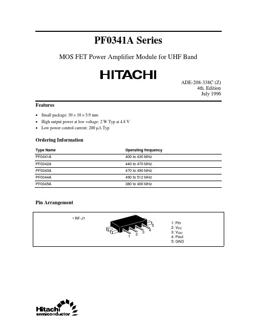
PF0341A SeriesMOS FET Power Amplifier Module for UHF BandADE-208-338C (Z)4th. EditionJuly 1996 Features• Small package: 30 × 10 × 5.9 mm• High output power at low voltage: 2 W Typ at 4.8 V• Low power control current: 200 µA TypOrdering InformationType Name Operating frequencyPF0341A400 to 430 MHzPF0342A440 to 470 MHzPF0343A470 to 490 MHzPF0344A490 to 512 MHzPF0345A380 to 400 MHzPin ArrangementPF0341A Series2Internal Diagram and External CircuitAbsolute Maximum Ratings (Tc = 25°C)ItemSymbol Rating Unit Supply voltage V DD 17V Supply current I DD 3A PC voltage V PC 4.5V Input powerPin 50mW Operating case temperature Tc (op)–30 to +100°C Storage temperatureTstg–40 to +110°CPF0341A Series3Electrical Characteristics (Tc = 25°C)ItemSymbol Min Typ Max Unit Test Condition Drain cutoff current I DS ——100µA V DD = 17 V, V PC = 0 V,R L = Rg = 50 Ω,Total efficiency ηT3538—%Pin = 20 mW, V DD = 9.6 V,2nd harmonic distortion 2nd H.D.—–30–25dBc Pout = 7 W (at V PC controlled),3rd harmonic distortion 3rd H.D.—–60–40dBc R L = Rg = 50 Ω, Tc = 25°CInput VSWR VSWR (in)— 2.0 3.0—Output power (1)Pout (1)78—W Pin = 20 mW, V DD = 9.6 V,V PC = 3.5 V, R L = Rg = 50 ΩOutput power (2)Pout (2) 1.82—W Pin = 20 mW, V DD = 4.8 V,V PC = 3.5 V, R L = Rg = 50 ΩLoad VSWR tolerance—No degradation—Pin = 20 mW, V DD = 15 V,Pout ≤ 7 W, (at V PC controlled),Output VSWR = 6:1 All phases Stability —No parasitic oscillation —Pin = 20 mW, V DD = 4.8 to 15 V,Pout ≤ 7 W, (at V PC controlled),Output VSWR = 6:1 All phases Mechanical CharacteristicsItemMeasuring Conditions SpecTorque for screw up the heatsink flange M2.6 Screw Bolts1.5 to 3.5 kg•cm Warp size of the heatsink flange: SS = 0+0.1/–0 mmPF0341A Series Characteristics Curve4PF0341A Series5PF0341A Series6PF0341A Series7PF0341A Series8PF0341A Series9PF0341A Series10PF0341A Series Package DimensionsUnit: mm11Cautions1.Hitachi neither warrants nor grants licenses of any rights of Hitachi’s or any third party’s patent,copyright, trademark, or other intellectual property rights for information contained in this document.Hitachi bears no responsibility for problems that may arise with third party’s rights, including intellectual property rights, in connection with use of the information contained in this document.2.Products and product specifications may be subject to change without notice. Confirm that you have received the latest product standards or specifications before final design, purchase or use.3.Hitachi makes every attempt to ensure that its products are of high quality and reliability. However,contact Hitachi’s sales office before using the product in an application that demands especially high quality and reliability or where its failure or malfunction may directly threaten human life or cause risk of bodily injury, such as aerospace, aeronautics, nuclear power, combustion control, transportation,traffic, safety equipment or medical equipment for life support.4.Design your application so that the product is used within the ranges guaranteed by Hitachi particularly for maximum rating, operating supply voltage range, heat radiation characteristics, installationconditions and other characteristics. Hitachi bears no responsibility for failure or damage when used beyond the guaranteed ranges. Even within the guaranteed ranges, consider normally foreseeable failure rates or failure modes in semiconductor devices and employ systemic measures such as fail-safes, so that the equipment incorporating Hitachi product does not cause bodily injury, fire or other consequential damage due to operation of the Hitachi product.5.This product is not designed to be radiation resistant.6.No one is permitted to reproduce or duplicate, in any form, the whole or part of this document without written approval from Hitachi.7.Contact Hitachi’s sales office for any questions regarding this document or Hitachi semiconductor products.Hitachi, Ltd.Semiconductor & IC Div.Nippon Bldg., 2-6-2, Ohte-machi, Chiyoda-ku, Tokyo 100-0004, Japan Tel: Tokyo (03) 3270-2111 Fax: (03) 3270-5109Copyright © Hitachi, Ltd., 1998. All rights reserved. Printed in Japan.Hitachi Asia Pte. Ltd.16 Collyer Quay #20-00Hitachi TowerSingapore 049318Tel: 535-2100Fax: 535-1533URLNorthAmerica : http:/Europe : /hel/ecg Asia (Singapore): .sg/grp3/sicd/index.htm Asia (Taiwan): /E/Product/SICD_Frame.htm Asia (HongKong): /eng/bo/grp3/index.htm Japan : http://www.hitachi.co.jp/Sicd/indx.htmHitachi Asia Ltd.Taipei Branch Office3F, Hung Kuo Building. No.167, Tun-Hwa North Road, Taipei (105)Tel: <886> (2) 2718-3666Fax: <886> (2) 2718-8180Hitachi Asia (Hong Kong) Ltd.Group III (Electronic Components)7/F., North Tower, World Finance Centre,Harbour City, Canton Road, Tsim Sha Tsui,Kowloon, Hong Kong Tel: <852> (2) 735 9218Fax: <852> (2) 730 0281 Telex: 40815 HITEC HXHitachi Europe Ltd.Electronic Components Group.Whitebrook ParkLower Cookham Road MaidenheadBerkshire SL6 8YA, United Kingdom Tel: <44> (1628) 585000Fax: <44> (1628) 778322Hitachi Europe GmbHElectronic components Group Dornacher Straße 3D-85622 Feldkirchen, Munich GermanyTel: <49> (89) 9 9180-0Fax: <49> (89) 9 29 30 00Hitachi Semiconductor (America) Inc.2000 Sierra Point Parkway Brisbane, CA 94005-1897Tel: <1> (800) 285-1601Fax: <1> (303) 297-0447For further information write to:。