自动往返电动小汽车设计
- 格式:pdf
- 大小:9.79 MB
- 文档页数:59
![基于plc的小车自动往返运动控制系统设计毕业设计[管理资料]](https://img.taocdn.com/s1/m/654db0f2c281e53a5902ff09.png)


开题报告电气工程及其自动化基于单片机的自动往返小汽车的设计一、综述本课题国内外研究动态,说明选题的依据和意义随着汽车工业的迅速发展,其与电子信息产业的融合速度也显著提高,汽车开始向电子化、多媒体化和智能化方向发展,使其不仅作为一种代步工具、同时能具有交通、娱乐、办公和通讯等多种功能。
关于汽车的研究也就越来越受人关注。
全国电子大赛和省内电子大赛几乎每次都有智能小车这方面的题目,全国各高校也都很重视该题目的研究。
可见其研究意义很大。
本设计就是在这样的背景下提出的,为了适应机电一体化的发展在汽车智能化方向的发展要求,提出简易智能小车的构想,目的在于:通过独立设计并制作一辆具有简单智能化的简易小车,获得项目整体设计的能力,并掌握多通道多样化传感器综合控制的方法。
设计的智能电动小车应该能够具有自动寻迹、小灯显示等功能。
由于单片机教学例子有限,因此,单片机智能车能综合学生课堂上的知识来实践,使学习者更好的了解单片机的发展。
通过此次的单片机寻轨车制作,使学生从理论到实践,初步体会单片机项目的设计、制作、调试和成功完成项目的过程及困难,以此学会用理论联系实际。
通过对实践中出现的不足与学习来补充教学上的盲点。
智能汽车是一种高新技术密集的新型汽车,是在网络环境下利用信息技术、智能控制技术、自动控制、模式识别、传感器技术、汽车电子、电气、计算机和机械等多个学科的最新科技成果,使汽车具有自动识别行驶道路、自动驾驶等先进功能.随着控制技术、计算机技术和信息技术的发展,智能车在工业生产和日常生活中已经扮演了非常重要的角色.近年来,智能车在野外、道路、现代物流及柔性制造系统中都有广泛运用,已成为人工智能领域研究和发展的热点。
二、研究的基本内容。
智能寻迹小车采用后轮驱动,左右后轮各用一个直流减速电机驱动,通过调制后面两个轮子的转速从而达到控制转向的目的在车体前部分别装有左中右三或者两个红外反射式传感器,当小车左边的传感器检测到黑线时,说明小车车头向右边偏移,这时主控芯片控制左轮电机减速,车体向左边修正同理当小车的右边传感器检测到黑线时,主控芯片控制右轮电机减速,车体向右边修正当黑线在车体的中间,中间的传感器一直检测到黑线,这样小车就会沿着黑线一直行走。

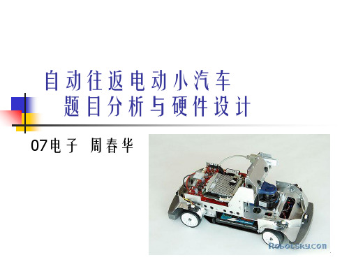
一. 毕业实践任务书无锡职业技术学院毕业实践任务书课题名称:自动往返电动小汽车指导教师:XXXXXXX 职称:讲师指导教师:职称:专业名称:XXXXXXXX 班组:XXXXXX学生姓名:XXXXXXX 学号:05一. 课题需要完成的任务:设计并制作一个能自动往返于起跑线与终点线间的小汽车。
允许用玩具汽车改装,但不能用人工遥控(包括有线和无线遥控)。
图1跑道顶视图跑道宽度0.5m,表面贴有白纸,两侧有挡板,挡板与地面垂直,其高度不低于20cm。
在跑道的B、C、D、E、F、G各点处画有2cm宽的黑线,各段的长度如图1所示。
设计要求1、车辆从起跑线出发(出发前,车体不得超出起跑线),到达终点线后停留10秒,然后自动返回起跑线(允许倒车返回)。
往返一次的时间应力求最短(从合上汽车电源开关开始计时)。
2. 达终点线和返回起跑线时,停车位置离起跑线和终点线偏差应最小(以车辆中心点与终点线或起跑线中心线之间距离作为偏差的测量值)。
D~E间为限速区,车辆往返均要求以低速通过,通过时间不得少于8秒,但不允许在限速区内停车。
二. 课题计划:2006.3.3~2006.3.6 熟悉课题,可行性方案分析及方案论述。
2006.3.7~2006.3.19 查阅资料,设计各部分硬件。
2006.3.19~2006.4.10 画原理图,印刷线路板。
2006.4.10~2006.4.20 编写程序验证部分硬件。
2006.4.21~2006.4.25 写出毕业论文。
计划答辩时间:4.21-4.28XXXXX 系(部、分院)2006年02年18日二.外文翻译VIDEOCASSETTEBefore the videocassette recorder there was the movie projector and screen. Perhaps you remember your fifth-grade teacher pulling down a screen—or Dad hanging a sheet on the wall, ready to show visiting friends the enthralling account of your summer vacation at the shore. Just as the film got started, the projector bulb often blew out.Those days did have one advantage, though: the screen was light, paper-thin and could be rolled into a portable tube. Compare that with bulky television and computer screens, and the projector screen invokes more than just nostalgia. Could yesterday's convenience be married to today's technology?The answer is yes, thanks to organic light-emitting materials that promise to make electronic viewing more convenient and ubiquitous. Used in displays, the organic materials are brighter, consume less energy and are easier to manufacture (thus potentially cheaper) than current options based on liquid crystals. Because organic light-emitting diodes (OLEDs) emit light, they consume significantly less power, especially in small sizes, than common liquid-crystal displays (LCDs), which require backlighting. OLEDs also offer several exciting advantages over common LEDs: the materials do not need to be crystalline (that is, composed of a precisely repeating pattern of planes of atoms), so they are easier to make; they are applied in thin layers for a slimmer profile; and different materials (for different colors) can be patterned on a given substrate to make high-resolution images. The substrates may be inexpensive glass or flexible plastic or even metal foil.In the coming years, large-screen televisions and computer monitors could roll up for storage. A soldier might unfurl a sheet of plastic showing a real-time situation map. Smaller displays could be wrapped around a person's forearm or incorporated into clothing. Used in lighting fixtures, the panels could curl around an architectural column or lie almost wallpaperlike against a wall or ceiling.LEDs currently have longer lifetimes than organic emitters, and itwill be tough to beat the widespread LED for use in indicator lamps. But OLEDs are already demonstrating their potential for displays. Their screens put out more than 100 candelas per square meter (about the luminance of a notebook screen) and last tens of thousands of hours (several years of regular use) before they dim to half their original radiance.Close to 100 companies are developing applications for the technology, focusing on small, low-power displays [see box on page 80]. Initial products include a nonflexible 2.2-inch (diagonal) display for digital cameras and cellular phones made jointly by Kodak and Sanyo, introduced in 2002, and a 15-inch prototype computer monitor produced by the same collaborative venture. The global market for organic display devices was about $219 million in 2003 and is projected to jump to $3.1 billion by 2009, according to Kimberly Allen of iSuppli/Stanford Resources, a market-research firm specializing in displays.一、What LED to OLEDCRYSTALLINE semiconductors—the forerunners of OLEDs—trace their roots back to the development of the transistor in 1947, and visible-light LEDs were invented in 1962 by Nick Holonyak, Jr. They were first used commercially as tiny sources of red light in calculators and watches and soon after also appeared as durable indicator lights of red, green or yellow. (When suitably constructed, LEDs form lasers, which have spawned the optical-fiber revolution, as well as optical data storage on compact discs and digital video discs.) Since the advent of the blue LED in the 1990s [see “Blue Chip,” by Glenn Zorpette; Scientific American, August 2000], full-color, large-screen television displays made from hundreds of thousands of LED chips have appeared in spectacular fashion on skyscrapers and in arenas [see “In Pursuit of the Ultimate Lamp,” by M. George Crawford, Nick Holonyak, Jr., and Frederick A. Kish, Jr.; Scientific American, February 2001]. Yet the smaller sizes used in devices such as PDAs (personal digital assistants) and laptops are not as practical.LEDs and OLEDs are made from layers of semiconductors—materials whose electrical performance is midway between an excellent conductorsuch as copper and an insulator such as rubber. Semiconducting materials, such as silicon, have a small energy gap between electrons that are bound and those that are free to move around and conduct electricity. Given sufficient energy in the form of an applied voltage, electrons can “jump” the gap a nd begin moving, constituting an electrical charge. A semiconductor can be made conductive by doping it; if the atoms added to a layer have a smaller number of electrons than the atoms they replace, electrons have effectively been removed, leaving positively charged “holes” and making the material “p-type.” Alternatively, a layer that is doped so that it has an excess of negatively charged electrons becomes “n-type” [see box on opposite page]. When an electron is added to a p-type material, it may encounter a hole and drop into the lower band, giving up an amount of energy (equal to the energy gap) as a photon of light. The wavelength depends on the energy gap of the emitting material.For the production of visible light, organic materials should have an energy gap between their lower and higher conduction bands in a relatively small range, about two to three electron volts. (One electron volt is defined as the kinetic energy gained by an electron when it is accelerated by a potential difference of one volt. A photon with one electron volt of energy corresponds to the infrared wavelength of 1,240 nanometers, and a photon of two electron volts has a wavelength half as much—620 nanometers—a reddish color.)二、A Surprising GlowORGANIC semiconductors are formed as aggregates of molecules that are, in the technologies being pursued, amorphous—a solid material, but one that is noncrystalline and without a definite order. There are two general types of organic light emitters, distinguished by “small” and “large” molecule sizes. The first practical p-n-type organic LED, based on small molecules, was invented in 1987 by Ching W. Tang and Steven A. Van Slyke of Eastman Kodak, after Tang noticed a surprising green glow coming from an organic solar cell he was working on. The duo recognized that by using two organic materials, one a good conductor of holes and the other a good conductor of electrons, they could ensure that photon emission would take place near the contact area, or junction, of the two materials, as in acrystalline LED. They also needed a material that held its electrons tightly, meaning that it would be easy to inject holes. For the light to escape, one of the contacts must be transparent, and the scientists benefited from the fortunate fact that the most widely used transparent conducting material, indium tin oxide, bound its electrons suitably for p-type contact material.The structure they came up with has not changed much over the years and is often called “Kodak-type,” because Kodak had the basic patent [see box on opposite page]. Beginning with a glass substrate, different materials are deposited layer by layer. This process is accomplished by evaporating the constituent materials and letting them condense on the substrate. The total thickness of the organic layers is only 100 to 150 nanometers, much thinner than that of a conventional LED (which is at least microns in thickness) and less than 1 percent of the thickness of a human hair. Because the molecules of the materials used are relatively lightweight—even lighter than a small protein—the Kodak-type OLEDs are referred to as “small molecule” OLEDs.After their initial insight, Tang and Van Slyke tinkered with the design to increase efficiency. They added a small amount of the fluorescent dye coumarin to the emitter material tris (8-hydroxy-quinoline) aluminum. The energy released by the recombination of holes and electrons was transferred to the dye, which emitted light with greatly increased efficiency. Deposition of additional thin layers of indium tin oxide and other compounds next to the electrodes altered the interaction of the thicker layers and also improved the efficiency of the injection of holes and electrons, thereby further upping the overall power efficiency of the fluorescent OLED.Organic LEDs of this small-molecule type are used to make red, green and blue light, with green light having the highest efficiency. Such green-emitting OLEDs can exhibit luminous efficiencies of 10 to 15 candelas per ampere—about as efficient as commercial LEDs today—and seven to 10 lumens per watt, values that are comparable to those for common incandescent lamps.录像机在卡匣式录像机出来之前,我们用的是电影放映机与屏幕。

自动往返电动小汽车余密刘勇尹佳喜华中科技大学电工电子创新中心(武汉430074)摘要:本设计以凌阳16位单片机SPCE061A为核心,通过高灵敏度红外光电传感器检测路面上的黑线,并进行计数,从而控制不同路段的速度,以红外对管检测车轮转动周数,根据车轮周长计算出速度及小车行驶路程。
单片机对高灵敏度红外光电传感器检测得到的路面信息进行处理后产生PWM输出,从而控制小车前轮与后轮电机转速,也就控制了小车的速度。
到达终点后,电机端电压反向,则小车行驶方向反向,小车由原路倒退返回。
红外对管检测到的小车车速及行驶路程信息经单片机计算处理后由液晶显示。
关键字:PWM 光电传感器检测调速一方案论证与选择1 电机调速模块电机调速主要是控制小车的速度与行驶方向。
通过对前轮电机转速的控制可控制小车的行驶方向,对小车的行驶速度的控制通过对其后轮转速的控制实现。
此模块为本设计的核心部分。
(1)电机调速方案方案一:电枢回路串电阻调速。
如II-1-1所示,通过单片机控制继电器,这样可以控制接入电枢回路电阻的大小,从而实现串电阻调速。
此方案只能分级调速,而且,串入电阻造成能量损耗,而本设计采用电池供电,显然,需要节能的调速系统,故此方案不能达到要求。
图III-1-1 电机电枢回路串电阻调速电路图方案二:电枢回路串电感调速。
原理图与方案一相同,将电阻换为电感,这样可以减小能耗,但由于电感消耗无功功率,造成电源污染,故不能采用此方案。
方案三:采用弱磁调速,即改变电机气隙磁通。
此方案可以连续调速,而且,能耗小,可由额定转速向高速方向调节,也可由额定转速向低速方向调节。
但由于小车电机不为他励直流电机,故很难改变磁通大小,方案难以实现。
方案四:采用改变端电压调速。
根据直流电机机械特性方程n=U a/k eФ+(R a+R j)T/k e k TФ2=n0-βT Tn——电机转速;n0——电机空载转速;k e、k T——电机结构参数所确定的电机电势常数、转矩常数;Ф——气隙磁通;U a——电动机电枢电压;R a、R j——电机电枢电阻及串入电阻;T——负载转矩;βT——机械特性曲线斜率;由上述直流电动机机械特性知,改变电枢端电压,可以连续改变电动机转速。
题目自动往返小车设计目录自动往返小车设计一、方案的选择与论证根据题目要求,系统可以划分为几个基本模块,如图 1所示。
图 1对各模块的实现,分别有以下一些不同的设计方案:1. 电动机驱动调速模块方案一:采用电阻网络或数字电位器调整电动机的分压,从而达到调速的目的。
但是电阻网络只能实现有级调速,而数字电阻的元器件价格比较昂贵。
更主要的问题在于一般电动机的电阻很小,但电流很大;分压不仅会降低效率,而且实现很困难。
方案二:采用继电器对电动机的开或关进行控制,通过开关的切换对小车的速度进行调整。
这个方案的优点是电路较为简单,缺点是继电器的响应时间慢、机械结构易损坏、寿命较短、可靠性不高。
方案三:采用由达林顿管组成的H型PWM电路。
用单片机控制达林顿管使之工作在占空比可调的开关状态,精确调整电动机转速。
这种电路由于工作在管子的饱和截止模式下,效率非常高;H型电路保证了可以简单地实现转速和方向的控制;电子开关的速度很快,稳定性也极强,是一种广泛采用的PWM调速技术。
基于上述理论分析,拟选择方案三。
2. 路面黑线探测模块探测路面黑线的大致原理是:光线照射到路面并反射,由于黑线和白纸的反射系数不同,可根据接收到的反射光强弱判断是否到达黑线。
方案一:可见光发光二极管与光敏二极管组成的发射-接收电路。
这种方案的缺点在于其他环境光源会对光敏二极管的工作产生很大干扰,一旦外界光亮条件改变,很可能造成误判和漏判;虽然采取超高亮发光管可以降低一定的干扰,但这又将增加额外的功率损耗。
方案二:不调制的反射式红外发射-接收器。
由于采用红外管代替普通可见光管,可以降低环境光源干扰;但如果直接用直流电压对管子进行供电,限于管子的平均功率要求,工作电流只能在1OM左右,仍然容易受到干扰。
方案三:脉冲调制的反射式红外发射-接收器。
考虑到环境光干扰主要是直流分量,如果采用带有交流分量的调制信号,则可大幅度减少外界干扰;另外,红外发射管的最大工作电流取决于平均电流,如果使用占空比小的调制信号,在平均电流不变的情况下,瞬时电流可以很大(50-100mA),这样也大大提高了信噪比。
自动往返电动小汽车本设计民用STM32作为自动往返小汽车的检测和控制核心,辅以传感器、控制电路、显示电路等外围器件,构成了一个车载控制系统。
路面黑线检测使用反射式红外传感器,利用PWM技术动态控制电动机的转速。
基于这些完备而可靠的硬件设计,使用了一套独特的软件算法,实现了小车在限速和压线过程中的精确控制。
电动小汽车能够根据题目要求在直线方向上完成调速、急刹车、停车、倒车返回等各种运动形式;这辆小车还可以自动记录、显示一次往返时间和行驶距离,并用蜂鸣器提示返回起点。
另外,我们经过MATLAB仿真后,成功地实现了从最高速降至低速的平稳调速。
本系统主要采用模糊控制算法进行速度调节。
通过模糊控制和PWM脉宽调制技术的结合,提高了对车位置控制精度,并且实现了恒速控制。
关键词:PWM,STM32F103,电机,传感器前言嵌入式技术依靠其体积小、成本低、功能强等特点,适应了智能化发展的最新要求。
单片机作为控制系统的微处理器,在数据处理和代码存储等方面都已经无法满足系统的要求,ARM微处理器资源丰富,具有良好的通用性。
Cortex-M3是ARM公司最新推出的第一款基于ARMv7体系的处理器内核。
它主要针对MCU领域,在存储系统、中断系统、调试接口等方面做了较大的改进,有别于过去的ARM7处理器;Cortex-M3具有高性能、低功耗、极低成本、稳定等诸多优点,非常适合汽车电子、工业控制系统、医疗器械、玩具等领域。
基于Cortex-M3内核的STM32系列处理器于2007年由ST公司率先推出,它集先进Cortex-M3内核结构、出众创新的外设、良好的功耗和低成本于一体,极大的满足自动控制系统设计要求。
作为先进的32位通用微控制器的领跑者,STM32以其出众的性能、丰富且灵活的外设、很高的性价比以及令人意外的功耗水准,使其自面世以来得到众多设计者的青睐,众多行业领导者纷纷选用STM32作为新一代产品的平台。
因此将STM32F103应用于智能小车的控制系统是一种较好的选择。
课程设计题目:小车自动往返系统设计学生姓名:学号:所在学院:专业班级:级别:指导教师:目录1 概述 (2)1.1 继电器-接触器控制系统的概况 (2)1.2 继电器与接触器的定义与概念 (2)1.3 继电器-接触器控制系统的优缺点 (3)1.4 继电器-接触器控制系统的发展形势 (3)2 方案设计 (3)2.1 控制系统描述 (3)2.3 继电器-接触器控制系统设计分析 (4)3 元器件的选型 (4)3.1 三相异步电动机的选择 (5)3.2 开关的选择 (5)3.3 熔断器的选择 (6)3.4 时间继电器的选择 (7)3.5 热继电器的选择 (7)3.6 接触器的选择 (8)4 电路图设计 (10)4.1主电路图 (10)4.2工作原理 (11)设计小结 (12)感谢 (13)参考文献 (14)附录一接线图 (15)附录二实物连接图 (16)1概述1.1继电器-接触器控制系统的概况电气控制课程是材料成型与控制工程专业的专业基础课,是由继电接触器控制系统来实现的。
它包含控制线路、主电路、照明电路及辅助线路组成。
该系统是由接触器、继电器、主令电器和保护电器等元件组成,按照一定的控制逻辑接线组成的控制系统。
其工作原理就是采用硬接线逻辑,利用继电器触点的串联或并联,及延时继电器的滞后动作等组成控制逻辑,从而实现对电动机或其他机械设备的起动、停止、反向、调速及对多台设备的顺序控制和自动保护功能。
1.2继电器与接触器的定义与概念接触器:由于接触器具有可控叫大容量,自身活动性质稳定,功能可靠,工作效率高及给够经久耐用等特性不仅被广泛应用在远距离操控高频度接断电路,一级容量较大甚至兼具负荷的各种系统物质中,比如各种电热机械装置、电焊机、电动机等,而且由于接触器可以进行自动控制一级齐纳电压情况下的释放作业保护型调节,所以,在各种进行远距离自动操控中也被作为一种电磁式自动调控开关进行使用。
如果我们将接触器一句自身结构的主触头所通电流进行划分可以得到:甲流接触器和直流接触器两种类别,其中前者种类较为多,而且就我国而言现有常用的租住设计并以进行投产的交流接触器组要有CJ10以及CJ20等系列型号。