
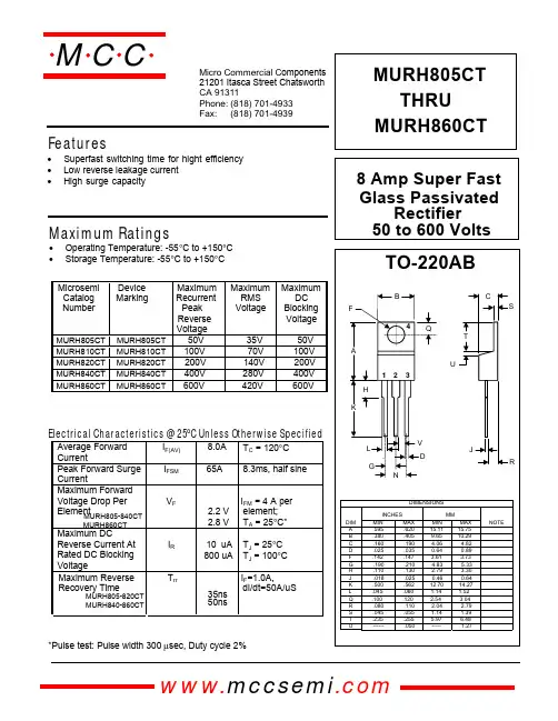
MURH820CT中文资料
- 格式:pdf
- 大小:148.79 KB
- 文档页数:2

MAX809 Series,MAX810 SeriesVery Low Supply Current3−Pin MicroprocessorReset MonitorsThe MAX809 and MAX810 are cost−effective system supervisor circuits designed to monitor V CC in digital systems and provide a reset signal to the host processor when necessary. No external components are required.The reset output is driven active within 10 m sec of V CC falling through the reset voltage threshold. Reset is maintained active for a timeout period which is trimmed by the factory after V CC rises above the reset threshold. The MAX810 has an active−high RESET output while the MAX809 has an active−low RESET output. Both devices are available in SOT−23 and SC−70 packages.The MAX809/810 are optimized to reject fast transient glitches on the V CC line. Low supply current of 0.5 m A (V CC= 3.2 V) makes these devices suitable for battery powered applications.Features•Precision V CC Monitor for 1.5 V, 1.8 V, 2.5 V, 3.0 V, 3.3 V, and 5.0 V Supplies•Precision Monitoring V oltages from 1.2 V to 4.9 V Availablein 100 mV Steps•Four Guaranteed Minimum Power−On Reset Pulse Width Available (1 ms, 20 ms, 100 ms, and 140 ms)•RESET Output Guaranteed to V CC = 1.0 V.•Low Supply Current•Compatible with Hot Plug Applications•V CC Transient Immunity•No External Components•Wide Operating Temperature: −40°C to 105°C•Pb−Free Packages are AvailableTypical Applications•Computers•Embedded Systems•Battery Powered Equipment•Critical Microprocessor Power Supply MonitoringV CCFigure 1. Typical Application DiagramSee general marking information in the device marking section on page 8 of this data sheet.DEVICE MARKING INFORMATIONSee detailed ordering and shipping information in the package dimensions section on page 8 of this data sheet.ORDERING INFORMATIONPIN DESCRIPTIONPin No.Symbol Description1GND Ground2RESET (MAX809)RESET output remains low while V CC is below the reset voltage threshold, and for a reset timeoutperiod after V CC rises above reset threshold2RESET (MAX810)RESET output remains high while V CC is below the reset voltage threshold, and for a reset timeoutperiod after V CC rises above reset threshold3V CC Supply Voltage (Typ)ABSOLUTE MAXIMUM RATINGSRating Symbol Value Unit Power Supply Voltage (V CC to GND)V CC−0.3 to 6.0V RESET Output Voltage (CMOS)−0.3 to (V CC + 0.3)V Input Current, V CC20mA Output Current, RESET20mAdV/dt (V CC)100V/m secThermal Resistance, Junction−to−Air (Note 1)SOT−23SC−70R q JA301314°C/WOperating Junction Temperature Range T J−40 to +105°C Storage Temperature Range T stg−65 to +150°C Lead Temperature (Soldering, 10 Seconds)T sol+260°C ESD ProtectionHuman Body Model (HBM): Following Specification JESD22−A114 Machine Model (MM): Following Specification JESD22−A1152000200VLatchup Current Maximum Rating: Following Specification JESD78 Class IIPositiveNegative I Latchup200200mAStresses exceeding Maximum Ratings may damage the device. Maximum Ratings are stress ratings only. Functional operation above the Recommended Operating Conditions is not implied. Extended exposure to stresses above the Recommended Operating Conditions may affect device reliability.1.This based on a 35x35x1.6mm FR4 PCB with 10mm2 of 1 oz copper traces under natural convention conditions and a single componentcharacterization.2.The maximum package power dissipation limit must not be exceeded.P D+T J(max)*T Aq JAwith T J(max) = 150°CELECTRICAL CHARACTERISTICS T A = −40°C to +105°C unless otherwise noted. Typical values are at T A = +25°C. (Note 3) Characteristic Symbol Min Typ Max Unit V CC RangeT A = 0°C to +70°CT A = −40°C to +105°C 1.01.2−−5.55.5VSupply CurrentV CC = 3.3 VT A = −40°C to +85°CT A = 85°C to +105°C V CC = 5.5 VT A = −40°C to +85°CT A = 85°C to +105°C I CC−−−−0.5−0.8−1.22.01.82.5m AReset Threshold (V in Decreasing) (Note 4)V TH V MAX809SN490T A = +25°CT A = −40°C to +85°C T A = +85°C to +105°C 4.834.784.664.9−−4.975.025.14MAX8xxLTR, MAX8xxSQ463T A = +25°CT A = −40°C to +85°C T A = +85°C to +105°C 4.564.504.404.63−−4.704.754.86MAX809HTRT A = +25°CT A = −40°C to +85°C T A = +85°C to +105°C 4.484.434.324.55 4.624.674.78MAX8xxMTR, MAX8xxSQ438T A = +25°CT A = −40°C to +85°C T A = +85°C to +105°C 4.314.274.164.38 4.454.494.60MAX809JTR, MAX8xxSQ400T A = +25°CT A = −40°C to +85°C T A = +85°C to +105°C 3.943.903.804.00−−4.064.104.20MAX8xxTTR, MAX809SQ308T A = +25°CT A = −40°C to +85°C T A = +85°C to +105°C 3.043.002.923.08−−3.113.163.24MAX8xxSTR, MAX8xxSQ293T A = +25°CT A = −40°C to +85°C T A = +85°C to +105°C 2.892.852.782.93−−2.963.003.08MAX8xxRTR, MAX8xxSQ263T A = +25°CT A = −40°C to +85°C T A = +85°C to +105°C 2.592.562.492.63−−2.662.702.77MAX809SN232, MAX809SQ232T A = +25°CT A = −40°C to +85°C T A = +85°C to +105°C 2.282.252.212.32−−2.352.382.45MAX809SN160T A = +25°CT A = −40°C to +85°C T A = +85°C to +105°C 1.581.561.521.60−−1.621.641.68MAX809SN120, MAX8xxSQ120T A = +25°CT A = −40°C to +85°C T A = +85°C to +105°C 1.181.171.141.20−−1.221.231.263.Production testing done at T A = 25°C, over temperature limits guaranteed by design.4.Contact your ON Semiconductor sales representative for other threshold voltage options.ELECTRICAL CHARACTERISTICS(continued) T A = −40°C to +105°C unless otherwise noted. Typical values are atT A = +25°C. (Note 5)Characteristic Symbol Min Typ Max Unit Detector Voltage Threshold Temperature Coefficient−30−ppm/°C V CC to Reset Delay V CC = V TH to (V TH − 100 mV)−10−m secReset Active TimeOut Period (Note 6) MAX8xxSN(Q)293D1MAX8xxSN(Q)293D2MAX8xxSN(Q)293D3MAX8xxSN(Q)293t RP1.020100140−−−−3.366330460msecRESET Output Voltage Low (No Load) (MAX809)V CC = V TH − 0.2 V1.6 V v V TH v2.0 V, I SINK = 0.5 mA2.1 V v V TH v 4.0 V, I SINK = 1.2 mA4.1 V v V TH v 4.9 V, I SINK = 3.2 mAV OL−−0.3VRESET Output Voltage High (No Load) (MAX809)V CC = V TH + 0.2 V1.6 V v V TH v2.4 V, I SOURCE = 200 m A2.5 V v V TH v 4.9 V, I SOURCE = 500 m AV OH0.8 V CC−−VRESET Output Voltage High (No Load) (MAX810)V CC = V TH + 0.2 V1.6 V v V TH v2.4 V, I SOURCE = 200 m A2.5 V v V TH v 4.9 V, I SOURCE = 500 m AV OH0.8 V CC−−VRESET Output Voltage Low (No Load) (MAX810)V CC = V TH − 0.2 V1.6 V v V TH v2.0 V, I SINK = 0.5 mA2.1 V v V TH v 4.0 V, I SINK = 1.2 mA4.1 V v V TH v 4.9 V, I SINK = 3.2 mAV OL−−0.3V5.Production testing done at T A = 25°C, over temperature limits guaranteed by design.6.Contact your ON Semiconductor sales representative for timeout options availability for other threshold voltage options.TYPICAL OPERATING CHARACTERISTICS0.50.40.30.20.10S U P P L Y C U R R E N T (m A )0.60.250.150.0500.35S U P P L Y C U R R E N T (m A )−50−2502550TEMPERATURE (°C)S U P P L Y C U R R E N T (m A )75100−50−2502550TEMPERATURE (°C)100Figure 6. Supply Current vs. Temperature(No Load, MAX809)Figure 7. Supply Current vs. Temperature (NoLoad, MAX810)750.100.200.30TYPICAL OPERATING CHARACTERISTICS252015105.00−50−25255075TEMPERATURE (°C)O U T P U T V O L T A G E V C C (m V )30100250−50−252575125TEMPERATURE (°C)125P O W E R −D O W N R E S E T D E L A Y (m s e c )125−50−2502550TEMPERATURE (°C)N O R M A L I Z E D P O W E R −U P R E S E T T I M E O U T0.70.80.91.21.375100Figure 10. Power−Down Reset Delay vs.Temperature and Overdrive (V TH = 1.2 V)Figure 11. Power−Down Reset Delay vs.Temperature and Overdrive (V TH = 4.9 V)Figure 12. Normalized Power−Up Reset vs.Temperature10050751.01.110050APPLICATIONS INFORMATIONV CC Transient RejectionThe MAX809 provides accurate V CC monitoring and reset timing during power−up, power−down, and brownout/sag conditions, and rejects negative−going transients (glitches) on the power supply line. Figure 13shows the maximum transient duration vs. maximum negative excursion (overdrive) for glitch rejection. Any combination of duration and overdrive which lies under the curve will not generate a reset signal. Combinations above the curve are detected as a brownout or power−down.Typically, transient that goes 100 mV below the reset threshold and lasts 5.0 m s or less will not cause a reset pulse.Transient immunity can be improved by adding a capacitor in close proximity to the V CC pin of the MAX809.Figure 13. Maximum Transient Duration vs.Overdrive for Glitch Rejection at 25°CV CC1011060M A X I M U M T R A N S I E N T D U R A T I O N (m s e c )RESET COMPARATOR OVERDRIVE (mV)410160210260310360RESET Signal Integrity During Power−DownThe MAX809 RESET output is valid to V CC = 1.0 V .Below this voltage the output becomes an “open circuit” and does not sink current. This means CMOS logic inputs to the Microprocessor will be floating at an undetermined voltage.Most digital systems are completely shutdown well above this voltage. However, in situations where RESET must bemaintained valid to V CC = 0 V , a pull−down resistor must be connected from RESET to ground to discharge stray capacitances and hold the output low (Figure 14). This resistor value, though not critical, should be chosen such that it does not appreciably load RESET under normal operation (100 k W will be suitable for most applications).Figure 14. Ensuring RESET Valid to V CC = 0 VProcessors With Bidirectional I/O PinsSome Microprocessor’s have bidirectional reset pins.Depending on the current drive capability of the processor pin, an indeterminate logic level may result if there is a logic conflict. This can be avoided by adding a 4.7 k W resistor in series with the output of the MAX809 (Figure 15). If there are other components in the system which require a reset signal, they should be buffered so as not to load the reset line.If the other components are required to follow the reset I/O of the Microprocessor, the buffer should be connected as shown with the solid line.Figure 15. Interfacing to Bidirectional Reset I/OBUFFERED RESETORDERING, MARKING AND THRESHOLD INFORMATIONPart Number V TH*(V)Timeout*(ms)Description Marking Package Shipping†MAX809SN160T1 1.60140−460Push−Pull RESET SAA SOT23−33000 / Tape & ReelMAX809SN160T1G 1.60140−460SAA SOT23−3(Pb−Free)MAX809SN232T1 2.32140−460SQP SOT23−3MAX809SN232T1G 2.32140−460SQP SOT23−3(Pb−Free)MAX809RTR 2.63140−460SPS SOT23−3MAX809RTRG 2.63140−460SPS SOT23−3(Pb−Free)MAX809STR 2.93140−460SPT SOT23−3MAX809STRG 2.93140−460SPT SOT23−3(Pb−Free)MAX809TTR 3.08140−460SPU SOT23−3MAX809TTRG 3.08140−460SPU SOT23−3(Pb−Free)MAX809JTR 4.00140−460SPR SOT23−3MAX809JTRG 4.00140−460SPR SOT23−3(Pb−Free)MAX809MTR 4.38140−460SPV SOT23−3MAX809MTRG 4.38140−460SPV SOT23−3(Pb−Free)MAX809HTR 4.55140−460SBD SOT23−3MAX809HTRG 4.55140−460SBD SOT23−3(Pb−Free)MAX809LTR 4.63140−460SPW SOT23−3MAX809LTRG 4.63140−460SPW SOT23−3(Pb−Free)MAX809SN490T1 4.90140−460SBH SOT23−3MAX809SN490T1G 4.90140−460SBH SOT23−3(Pb−Free)MAX809SN120T1G 1.20140−460SSO SOT23−3(Pb−Free)MAX809SN293D1T1G 2.931−3.3SSP SOT23−3(Pb−Free)MAX809SN293D2T1G 2.9320−66SSQ SOT23−3(Pb−Free)MAX809SN293D3T1G 2.93100−330SSR SOT23−3(Pb−Free)MAX809SQ120T1G 1.20140−460ZD SC70−3(Pb−Free)MAX809SQ232T1G 2.32140−460ZE SC70−3(Pb−Free)MAX809SQ263T1G 2.63140−460ZF SC70−3(Pb−Free)MAX809SQ293T1G 2.93140−460ZG SC70−3(Pb−Free)MAX809SQ308T1G 3.08140−460ZH SC70−3(Pb−Free)MAX809SQ400T1G 4.00140−460SZ SC70−3(Pb−Free)MAX809SQ438T1G 4.38140−460ZI SC70−3(Pb−Free)MAX809SQ463T1G 4.63140−460ZJ SC70−3(Pb−Free)MAX809SQ293D1T1G 2.931−3.3ZK SC70−3(Pb−Free)MAX809SQ293D2T1G 2.9320−66ZL SC70−3(Pb−Free)MAX809SQ293D3T1G 2.93100−330ZM SC70−3(Pb−Free)†For information on tape and reel specifications,including part orientation and tape sizes, please refer to our Tape and Reel Packaging Specifications Brochure, BRD8011/D.*Contact your ON Semiconductor sales representative for other threshold voltage options.ORDERING, MARKING AND THRESHOLD INFORMATIONPart Number V TH*(V)Timeout*(ms)Description Marking Package Shipping†MAX810RTR 2.63140−460Push−Pull RESET SPX SOT23−33000 / Tape & ReelMAX810RTRG 2.63140−460SPX SOT23−3(Pb−Free)MAX810STR 2.93140−460SPY SOT23−3MAX810STRG 2.93140−460SPY SOT23−3(Pb−Free)MAX810TTR 3.08140−460SPZ SOT23−3MAX810TTRG 3.08140−460SPZ SOT23−3(Pb−Free)MAX810MTR 4.38140−460SQA SOT23−3MAX810MTRG 4.38140−460SQA SOT23−3(Pb−Free)MAX810LTR 4.63140−460SQB SOT23−3MAX810LTRG 4.63140−460SQB SOT23−3(Pb−Free)MAX810SN120T1G 1.20140−460SSS SOT23−3(Pb−Free)MAX810SN293D1T1G 2.931−3.3SST SOT23−3(Pb−Free)MAX810SN293D2T1G 2.9320−66SSU SOT23−3(Pb−Free)MAX810SN293D3T1G 2.93100−330SSZ SOT23−3(Pb−Free)MAX810SQ120T1G 1.20140−460ZN SC70−3(Pb−Free)MAX810SQ263T1G 2.63140−460ZO SC70−3(Pb−Free)MAX810SQ293T1G 2.93140−460ZP SC70−3(Pb−Free)MAX810SQ438T1G 4.38140−460ZQ SC70−3(Pb−Free)MAX810SQ463T1G 4.63140−460ZR SC70−3(Pb−Free)MAX810SQ293D1T1G 2.931−3.3ZS SC70−3(Pb−Free)MAX810SQ293D2T1G 2.9320−66ZT SC70−3(Pb−Free)MAX810SQ293D3T1G 2.93100−330ZU SC70−3(Pb−Free)†For information on tape and reel specifications,including part orientation and tape sizes, please refer to our Tape and Reel Packaging Specifications Brochure, BRD8011/D.*Contact your ON Semiconductor sales representative for other threshold voltage options.PACKAGE DIMENSIONSSOT−23 (TO236)CASE 318−08ISSUE AN*For additional information on our Pb−Free strategy and solderingdetails, please download the ON Semiconductor Soldering and Mounting Techniques Reference Manual, SOLDERRM/D.SOLDERING FOOTPRINT*ǒmm inchesǓSCALE 10:1NOTES:1.DIMENSIONING AND TOLERANCING PER ANSI Y14.5M, 1982.2.CONTROLLING DIMENSION: INCH.3.MAXIMUM LEAD THICKNESS INCLUDES LEAD FINISH THICKNESS. MINIMUM LEADTHICKNESS IS THE MINIMUM THICKNESS OF BASE MATERIAL.4.318−01 THRU −07 AND −09 OBSOLETE, NEW STANDARD 318−08.VIEW CDIM A MIN NOM MAX MINMILLIMETERS0.89 1.00 1.110.035INCHES A10.010.060.100.001b 0.370.440.500.015c 0.090.130.180.003D 2.80 2.90 3.040.110E 1.20 1.30 1.400.047e 1.78 1.90 2.040.070L 0.100.200.300.0040.0400.0440.0020.0040.0180.0200.0050.0070.1140.1200.0510.0550.0750.0810.0080.012NOM MAX L1 2.102.40 2.640.0830.0940.104H E0.350.540.690.0140.0210.029MAX809 Series, MAX810 SeriesPACKAGE DIMENSIONSSC−70 (SOT−323)CASE 419−04ISSUE Mǒmm inchesǓSCALE 10:1*For additional information on our Pb−Free strategy and solderingdetails, please download the ON Semiconductor Soldering and Mounting Techniques Reference Manual, SOLDERRM/D.ON Semiconductor and are registered trademarks of Semiconductor Components Industries, LLC (SCILLC). SCILLC reserves the right to make changes without further notice to any products herein. SCILLC makes no warranty, representation or guarantee regarding the suitability of its products for any particular purpose, nor does SCILLC assume any liability arising out of the application or use of any product or circuit, and specifically disclaims any and all liability, including without limitation special, consequential or incidental damages.“Typical” parameters which may be provided in SCILLC data sheets and/or specifications can and do vary in different applications and actual performance may vary over time. All operating parameters, including “Typicals” must be validated for each customer application by customer’s technical experts. SCILLC does not convey any license under its patent rights nor the rights of others. SCILLC products are not designed, intended, or authorized for use as components in systems intended for surgical implant into the body, or other applications intended to support or sustain life, or for any other application in which the failure of the SCILLC product could create a situation where personal injury or death may occur. Should Buyer purchase or use SCILLC products for any such unintended or unauthorized application, Buyer shall indemnify and hold SCILLC and its officers, employees, subsidiaries, affiliates,and distributors harmless against all claims, costs, damages, and expenses, and reasonable attorney fees arising out of, directly or indirectly, any claim of personal injury or death associated with such unintended or unauthorized use, even if such claim alleges that SCILLC was negligent regarding the design or manufacture of the part. SCILLC is an Equal Opportunity/Affirmative Action Employer. This literature is subject to all applicable copyright laws and is not for resale in any manner.PUBLICATION ORDERING INFORMATION元器件交易网。
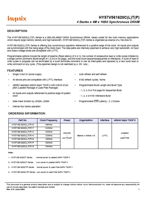

H820系列DTU规格说明书产品概述H820系列DTU是伊林思科技有限公司基于无线网络需求,采用最新硬件系统平台,使用Linux软件系统引用最新技术研发出来的一款全新的,性能更为优异的物联网无线通信DTU产品。
采用工业级设计标准,它主要应用于行业用户的数据传输业务。
H820为DTU+路由器二合一的数传设备。
该产品采用高性能的32位嵌入式处理器,内嵌完备的TCP/IP协议栈,同时提供RS串口和10/100M以太网接口。
集成IO端子座,提供串口或者GPIO接口。
串口分别提供RS-232、RS-485、TTL电平接口的透明传输模式,支持的VPN 通信功能,采用IPSec/PPTP/L2TP/GRE VPN技术,企业级VPN隧道技术和防火墙技术,保证高安全性行业的数据安全,支持自动在线检测,实时动态刷新网络状态,保持链路畅通,产品以性能稳定、体积小、易于安装嵌入、抵抗环境能力强等优点,深受用户欢迎。
支持WEB/Telnet/Console多种配置方式,其中用户面对的是WEB图形化管理配制界面,管理方便简单。
该产品已广泛应用于物联网产业链中的M2M 行业,如智能电网、智能交通、智能家居、金融、移动POS 终端、供应链自动化、工业自动化、智能建筑、消防、公共安全、环境保护、气象、数字化医疗、遥感勘测、军事、空间探索、农业、林业、水务、煤矿、石化等领域。
行业应用金融:银行储蓄点机房监控,移动性证券交易和信息查询通信:电信机房动力环境监控,通信维护人员线路资料查询交通:GPRS/SMS/GPS 机动车辆监控调度系统;银行运钞车,邮政运输车监控调度。
公安:公安、110、交警车辆监控调度,公安移动性数据(身份证、犯罪档案等)查询,交警移动通信数据(车辆、司机档案等)查询。
热力:热力系统实时监控和维护电力:电力系统城市中电网实时监控和自动补偿,远程自动抄表公司:移动办公及管理,其他外勤人员移动性数据查询工业:工业遥感,遥测,遥控信息回报气象:气象数据采集与传输水利:水文监测生活:煤气调压站实时数据采集自动控制,自来水,污水管道,闸门、泵站与水厂实时监控维护电子商务:支持B2B、B2C的电子商务和电子支付、股票交易等。

德国蔡司双焦点人工晶体809m参数【原创实用版】目录1.德国蔡司双焦点人工晶体 809m 简介2.人工晶体的重要性3.德国蔡司双焦点人工晶体 809m 的参数4.德国蔡司双焦点人工晶体 809m 的优势5.德国蔡司双焦点人工晶体 809m 的适用人群6.结论正文1.德国蔡司双焦点人工晶体 809m 简介德国蔡司双焦点人工晶体 809m 是一款由德国蔡司公司研发生产的人工晶体。
人工晶体是一种用于替代人眼自然晶体的医疗器械,能够在眼科手术中植入眼内,帮助患者恢复视力。
2.人工晶体的重要性人工晶体是眼科手术中非常重要的组成部分,可以替代人眼自然晶体,帮助患者恢复视力。
在白内障等眼科手术中,人工晶体的质量和性能直接影响着手术的效果和术后视力的恢复。
3.德国蔡司双焦点人工晶体 809m 的参数德国蔡司双焦点人工晶体 809m 的参数如下:- 折射率:1.90- 直径:8.9mm- 厚度:0.9mm- 光学区直径:6.0mm- 聚焦深度:0.8mm- 色散:0.114.德国蔡司双焦点人工晶体 809m 的优势德国蔡司双焦点人工晶体 809m 具有以下优势:- 高质量的材料:采用高品质的材料制成,具有良好的生物相容性和稳定性。
- 优秀的光学性能:具有较高的折射率和聚焦深度,能够提供良好的视力恢复效果。
- 双焦点设计:采用双焦点设计,能够同时提供远近两种视力,减少术后视觉疲劳。
5.德国蔡司双焦点人工晶体 809m 的适用人群德国蔡司双焦点人工晶体 809m 适用于以下人群:- 白内障患者:适用于白内障等眼科手术,能够替代人眼自然晶体,帮助患者恢复视力。
- 老花眼患者:适用于老花眼患者,能够提供远近两种视力,减少术后视觉疲劳。