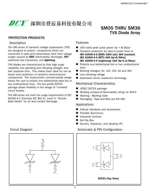
SM05 THRU SM36PROTECTION PRODUCTS TVS Diode ArrayDescriptionFeaturesCircuit Diagram Schematic & PIN ConfigurationThe SM series of transient voltage suppressors (TVS)are designed to protect components which areconnected to data and transmission lines from voltage surges caused by ESD (electrostatic discharge), EFT (electrical fast transients), and lightning .TVS diodes are characterized by their high surge capability, low operating and clamping voltages, and fast response time. This makes them ideal for use as board level protection of sensitive semiconductorcomponents. The dual-junction common-anode design allows the user to protect one bidirectional data line or two unidirectional lines. The low profile SOT23package allows flexibility in the design of crowded circuit boards.The SM series will meet the surge requirements of IEC 61000-4-2 (Formerly IEC 801-2), Level 4, Human Body Model for air and contact discharge.ApplicationsMechanical Characteristicsu Cellular Handsets and Accessories u Portable Electronics u Industrial Controls u Set-Top BoxuServers, Notebook, and Desktop PCu 300 watts peak pulse power (tp = 8/20µs)u Transient protection for data & power lines toIEC 61000-4-2 (ESD) 15kV (air), 8kV (contact)IEC 61000-4-4 (EFT) 40A (tp=5/50ns)IEC 61000-4-5 (Lightning) 12A (tp=1.2/50µs)u Protects one bidirectional line or two unidirectional linesu Working Voltages: 5V, 12V, 15V, 24 and 36V u Low clamping voltageu Solid-state silicon avalanche technologyu JEDEC SOT23 packageu Molding compound flammability rating: UL 94V-0u Marking : Marking Codeu Packaging : Tape and Reel per EIA 481Absolute Maximum RatingElectrical Characteristics50M S re t e m a r a P l o b m y S sn o i t i d n o C mu m i n i M la c i p y T mu m i x a M s t i n U e g a t l o V f f O -d n a t S e s r e v e R V M W R 5V e g a t l o V n w o d k a e r B e s r e v e R V R B I t A m 1=6V t n e r r u C e g a k a e L e s r e v e R I R V M W R C °52=T ,V 5=02A µeg a t l o V g n i p m a l C V C I P P ,A 1=s µ02/8=p t 8.9V t n e r r u C e s l u P k a e P m u m i x a M I p p s µ02/8=p t 71A e c n a t i c a p a C n o i t c n u J C j 2o t 1n i P V R z H M 1=f ,V 0=053F p ec n a t i c a p a C n o i t c n u J C jd n a 3o t 1n i P 3o t 2n i P V R zH M 1=f ,V 0=004Fp gn i t a R l o b m y S e u l a V s t i n U )s µ02/8=p t (r e w o P e s l u P k a e P P k p 003s t t a W t n e i b m A o t n o i t c n u J ,e c n a t s i s e R l a m r e h T q A J 655W /C °e r u t a r e p m e T g n i r e d l o S d a e L T L ).c e s 01(062C °e r u t a r e p m e T g n i t a r e p O T J 521+o t 55-C °er u t a r e p m e T e g a r o t S T GT S 051+o t 55-C°21M S re t e m a r a P l o b m y S sn o i t i d n o C mu m i n i M la c i p y T mu m i x a M s t i n U e g a t l o V f f O -d n a t S e s r e v e R V M W R 21V e g a t l o V n w o d k a e r B e s r e v e R V R B I t A m 1=3.31V t n e r r u C e g a k a e L e s r e v e R I R V M W R C°52=T ,V 21=1A µeg a t l o V g n i p m a l C V C I P P ,A 1=s µ02/8=p t 91V t n e r r u C e s l u P k a e P m u m i x a M I p p s µ02/8=p t 21A e c n a t i c a p a C n o i t c n u J C j 2o t 1n i P V R z H M 1=f ,V 0=021F p ec n a t i c a p a C n o i t c n u J C jd n a 3o t 1n i P 3o t 2n i P V R zH M 1=f ,V 0=051FpElectrical Characteristics (Continued)51M S re t e m a r a P l o b m y S s n o i t i d n o C m u m i n i M l a c i p y T mu m i x a M s t i n U e g a t l o V f f O -d n a t S e s r e v e R V M W R 51V e g a t l o V n w o d k a e r B e s r e v e R V R B I t A m 1=7.61Vt n e r r u C e g a k a e L e s r e v e R I R V M W R C °52=T ,V 51=1A µeg a t l o V g n i p m a l C V C I P P sµ02/8=p t ,A 1=42V t n e r r u C e s l u P k a e P m u m i x a M I p p s µ02/8=p t 01A e c n a t i c a p a C n o i t c n u J C j 2o t 1n i P V R z H M 1=f ,V 0=57F p e c n a t i c a p a C n o i t c n u J C j3o t 2d n a 3o t 1n i P V R zH M 1=f ,V 0=001Fp 42M S re t e m a r a P l o b m y S sn o i t i d n o C mu m i n i M l a c i p y T mu m i x a M s t i n U e g a t l o V f f O -d n a t S e s r e v e R V M W R 42V e g a t l o V n w o d k a e r B e s r e v e R V R B I t A m 1=7.62Vt n e r r u C e g a k a e L e s r e v e R I R V M W R C °52=T ,V 42=1A µeg a t l o V g n i p m a l C V C I P P sµ02/8=p t ,A 1=34V t n e r r u C e s l u P k a e P m u m i x a M I p p s µ02/8=p t 5A e c n a t i c a p a C n o i t c n u J C j 2o t 1n i P V R z H M 1=f ,V 0=05F p ec n a t i c a p a C n o i t c n u J C j3o t 2d n a 3o t 1n i P V R zH M 1=f ,V 0=06Fp 63M S re t e m a r a P l o b m y S s n o i t i d n o C m u m i n i M l a c i p y T mu m i x a M s t i n U e g a t l o V f f O -d n a t S e s r e v e R V M W R 63V e g a t l o V n w o d k a e r B e s r e v e R V R B I t A m 1=04Vt n e r r u C e g a k a e L e s r e v e R I R V M W R C °52=T ,V 63=1A µeg a t l o V g n i p m a l C V C I P P sµ02/8=p t ,A 1=06V t n e r r u C e s l u P k a e P m u m i x a M I p p s µ02/8=p t 4A e c n a t i c a p a C n o i t c n u J C j 2o t 1n i P V R z H M 1=f ,V 0=04F p ec n a t i c a p a C n o i t c n u J C j3o t 2d n a 3o t 1n i P V R zH M 1=f ,V 0=54FpTypical CharacteristicsNon-Repetitive Peak Pulse Power vs. Pulse Time1020304050607080901001100255075100125150Ambient Temperature - T A (oC)% o f R a t e d P o w e r o r I P PPower Derating CurvePulse Waveform0102030405060708090100110051015202530Time (µs)P e r c e n t o f I P Ple v e L t s r i F k a e P t n e r r u C )A (k a e P t n e r r u C s n 03t a )A (k a e P t n e r r u C s n 06t a )A (t s eT eg a t l o V tc a t n o C ()e g r a h c s i D )V k (ts e T e g a t l o V r i A ()e g r a h c s i D )V k (15.74822251844435.2221668436188510.010.11100.11101001000Pulse Duration - tp (µs)P e a k P u l s e P o w e r - P P P (k W )IEC 61000-4-2 Discharge ParametersESD Pulse Waveform (Per IEC 61000-4-2)Applications InformationDevice Schematic & Pin Configuration Device Connection OptionsThe SM series is designed to protect one bidirectionalor two unidirectional data or I/O lines operating at 5 to36 volts. Connection options are as follows:l Bidirectional: Pin 1 is connected to the data lineand pin 2 is connected to ground (Since the deviceis symmetrical, these connections may be re-versed). For best results, the ground connectionshould be made directly to a ground plane on theboard. The path length should be kept as short aspossible to minimize parasitic inductance. Pin 3 isnot connected.l Unidirectional: Data lines are connected to pin 1 and pin 2. Pin 3 is connected to ground. For best results, this pin should be connected directly to aground plane on the board. The path length should be kept as short as possible to minimize parasiticinductance.Circuit Board Layout Recommendations for Suppres-sion of ESD.Good circuit board layout is critical for the suppression of fast rise-time transients such as ESD. The following guidelines are recommended (Refer to application note SI99-01 for more detailed information):l Place the TVS near the input terminals or connec-tors to restrict transient coupling.l Minimize the path length between the TVS and the protected line.l Minimize all conductive loops including power and ground loops.l The ESD transient return path to ground should be kept as short as possible.l Never run critical signals near board edges.l Use ground planes whenever possible.RS-232 Transceiver ProtectionExampleOutline Drawing - SOT23Ordering Informationr e b m u N t r a P g n i k r o W e g a t l o V le e R r e p y t Q e z i S l e e R C T .50M S V 5000,3h c n I 7G T .50M S V 5000,01h c n I 31C T .21M S V 21000,3h c n I 7G T .21M S V 21000,01h c n I 31C T .51M S V 51000,3h c n I 7G T .51M S V 51000,01h c n I 31C T .42M S V 42000,3h c n I 7G T .42M S V 42000,01h c n I 31CT .63M S V63000,3hc n I 7Marking Codesre b m u N t r a P g n i k r a M e d o C 50M S 50M 21M S 21M 51M S 51M 42M S 42M 63M S 63M。